YAC520 CATALOG
CATALOG No.: LSI-4AC520A4
2001.12
YAC520
HGVC1
High Grade Volume Control
s
Outline
YAC520(HGVC1) is a high grade stereophonic digital volume for high end audio system.
It provides wide dynamic range and low distortion as well, and can control individual channels in 256
steps with 0.5 dB per step. The use of 16 bit serial data interface allows daisy chain connection of
several devices for multi channel system.
Zero Crossing Detection function suppresses audible noise at quick change of the volume.
YAC520 operates on a single 5 volt power supply, and it is possible to input signal of up to 7.9Vrms by
using three types of connection methods.
Development evaluation board, DMB-HGVC1, equipped with PC interface is available.
s
Features
q
Wide volume range
A: +32.0 to
≠
95.0dB IN1=IN2
(Input < 2.0Vrms @V
DD
=5V)
(can be used in three ways)
B: +29.5 to
≠
97.5dB IN2=GND
(Input < 2.6Vrms @V
DD
=5V)
C: +20.0 to
≠
107.0dB IN1=GND
(Input < 7.9Vrms @V
DD
=5V)
q
Adjustment step
adjustable in 256 steps, with 0.5dB per step
q
Gain Error
± 0.1dB
q
Low distortion factor
0.001% (input=150 mVrms, gain=+16dB)
q
Low residual noise
1
µ
Vrms (gain=- )
s
Others
Process CMOS
process
Package
20 SSOP (YAC520-E)
Power supply voltage
5 V
Operating temperature
0 to +70 ∫C
Power consumption
100 mW @V
DD
=5.0 V

YAC520
4
s
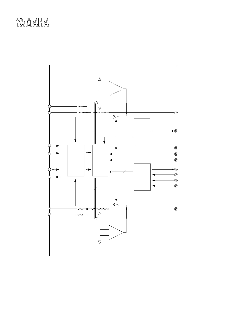
Pin Functions
∑
Power supply pins
Power supply pins
Power supply pins
Power supply pins
AVDD
AVDD
AVDD
AVDD
≠
≠
≠
≠
Analog power supply (+5.0 V)
AVSS
AVSS
AVSS
AVSS
≠
≠
≠
≠
Analog ground
DVDD
DVDD
DVDD
DVDD
≠
≠
≠
≠
Digital power supply (+5.0 V)
DVSS
DVSS
DVSS
DVSS
≠
≠
≠
≠
Digital ground
∑
Analog Pins
Analog Pins
Analog Pins
Analog Pins
LIN1
LIN1
LIN1
LIN1
≠
≠
≠
≠
Left Channel Analog input 1
Lch analog input pin 1
Gain setting ranges from +32 dB to
≠
95 dB when the signal inputted to LIN2 is inputted this pin, and
gain setting ranges from +20.0 dB to
≠
107.0 dB when it is grounded through a capacitor.
LIN2
LIN2
LIN2
LIN2
≠
≠
≠
≠
Left Channel Analog input 2
Lch analog input pin 2
Gain setting ranges from +32 dB to
≠
95 dB when the signal inputted to LIN1 is inputted this pin, and
gain setting ranges from +29.5 dB to
≠
97.5 dB when it is grounded through a capacitor.
RIN1
RIN1
RIN1
RIN1
≠
≠
≠
≠
Right Channel Analog input 1
Rch analog input pin 1
Gain setting ranges from +32 dB to
≠
95 dB when the signal inputted to RIN2 is inputted this pin, and
gain setting ranges from +20.0 dB to
≠
107.0 dB when it is grounded through a capacitor.
RIN2
RIN2
RIN2
RIN2
≠
≠
≠
≠
Right Channel Analog input 2
Rch analog input pin 2
Gain setting ranges from +32 dB to
≠
95 dB when the signal inputted to RIN1 is inputted this pin, and
gain setting ranges from +29.5 dB to
≠
97.5 dB when it is grounded through a capacitor.
LOUT
LOUT
LOUT
LOUT
≠
≠
≠
≠
Left Channel Analog output
Lch analog output pin
Note this is an inverted output.
ROUT
ROUT
ROUT
ROUT
≠
≠
≠
≠
Right Channel Analog output
Rch analog output pin
Note this is an inverted output.
VREF
VREF
VREF
VREF
≠
≠
≠
≠
Analog Reference Voltage (output)
Analog reference voltage output pin
Outputs 1/2VDD. Ground through a capacitor of 10
µ
F or more to attain stabilization.
∑
Digital Pins
Digital Pins
Digital Pins
Digital Pins
SDATAI
SDATAI
SDATAI
SDATAI
≠≠
≠≠
Serial Data Input
Serial data input pin
SDATAO
SDATAO
SDATAO
SDATAO
≠≠
≠≠
Serial Data Output
Serial data putput pin
Outputs Serial data when CSN is "low", or becomes high impedance state when it is "high".
SCLK
SCLK
SCLK
SCLK
≠
≠
≠
≠
Serial Clock (Input)
Serial clock input pin
CSN
CSN
CSN
CSN
≠
≠
≠
≠
Chip Select (Input)
Chip select input pin
ICN
ICN
ICN
ICN
≠
≠
≠
≠
DC Bias Initial Clear (Input)
DC bias initialization pin.
DC bias is set to VREF (analog reference voltage) when this is "low".
To stabilize the bias voltage at power on, determine the control time in accordance with the coupling
capacitor that is connected to the inputs (LIN1, LIN2, RIN1 ,RIN2).
(Refer to "VREF stabilization time and DC bias initialization time" in the description of functions.)
ZCEN
ZCEN
ZCEN
ZCEN
≠
≠
≠
≠
Zero Crossing Enable (Input)
Zero crossing control pin.
Making this pin "high" enables a mode where volume change is performed
after detecting zero crossing.
The volume change immediately after writing data when this pin is "low".
TE
TE
TE
TE
≠
≠
≠
≠
Test Enable (Input)
Test mode control pin.
Fix it to "low" or with NC when using.

YAC520
5
s
Description of analog functions
∑
Maximum input voltage
As described in the following figure, the maximum amplitude of signal that can be inputted varies
according the method of the use of L(R) IN1 and 2 pins. The method A makes the maximum
amplitude of the input signal approximately 2 Vrms, the method B makes it approximately 2.6 Vrms,
and the method C makes it approximately 7.9 Vrms. The use of the method B or C allows to input
signal exceeding the power supply voltage.
Note that the gain setting range for the method B is reduced by 2.5 dB from the one for the method A,
and 12 dB for the method C.
∑
VREF (analog reference voltage) stabilization time and DC bias initialization time
The time required for stabilization of VREF pin voltage after power on moment varies according to
the capacitance of the capacitor connected to VREF pin. Connecting a capacitor of 10
µ
F makes the
time constant 30 ms (typ.). Note that the serial interface becomes invalid in this period, t
PUP
.
As shown in the following figure, making ICN terminal "low" sets the DC bias forcibly with SW in the
LSI.
Since the time constant of L(R) IN1 and 2 pins becomes approximately 300 ms (typ.) when a
capacitor of 100
µ
F is used as the coupling capacitors (Ci1, 2), control ICN according to the capacitor
that is connected.
+
-
VREF
L(R)OUT
L(R) IN1
∑
∑ ∑ ∑
L(R) IN2
Ri(1)
Ri(2)
Rf
MethodA: IN1=IN2 Gain range (+32 dB to ≠95 dB)
Maximum input voltage: 2 Vrms
+
-
VREF
L(R)OUT
L(R) IN1
∑
∑ ∑ ∑
L(R) IN2
MethodB: IN2=GND Gain range (+29.5 dB to ≠97.5 dB)
Maximum input voltage: 2.6 Vrms
Ri(1)
Ri(2)
Rf
+
-
VREF
L(R)OUT
L(R) IN1
∑
∑ ∑ ∑
L(R) IN2
MethodC: IN1=GND Gain range (+20 dB to ≠107 dB)
Maximum input voltage: 7.9 Vrms
Ri(1)
Ri(2)
Rf
+
-
VREF
L(R)OUT
L(R) IN1
L(R) IN2
Ri1=0.98k
Ri2=2.94k
Rf=29.3k
Ci1
Ci2
ICN
Rsw= 80
(typ)
Gain setting after power on = -
Audio
Source
SW