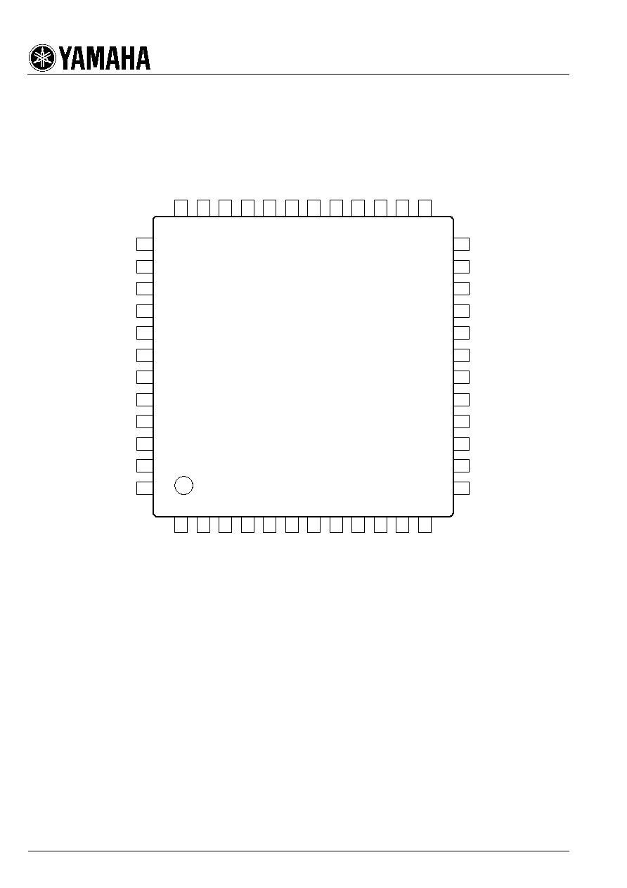
YAC523
3
Terminal function
AVSS
AVDD
IN1
IN2
IN3
IN4
IN5
IN6
IN7
AVSS
REF7B
No.
Name
I/O
Function
REF1A
REF2B
REF2A
REF3B
REF3A
REF4B
REF4A
REF5A
REF5B
REF6A
REF6B
REF7A
NC
NC
OUT1
OUT2
OUT3
OUT4
OUT6
OUT7
NC
NC
OUT5
REF1B
AVSS
ZCEN1
ZCEN2
CSN
SDATAI
SCLK
SDATAO
TE2
DGND
REF
AVSS
1
2
3
4
5
6
7
8
9
10
11
12
13
14
15
16
17
18
19
20
21
22
23
24
25
26
27
28
29
30
31
32
33
34
35
36
37
38
39
40
41
42
43
44
46
47
48
-
AI
AI
AI
AI
AI
AI
AI
AO
AO
AO
AO
AO
I
I
I
I
I
OD
I
O
Minus power supply for analog (-6.0V Typ.)
Plus power supply for analog (+6.0V Typ.)
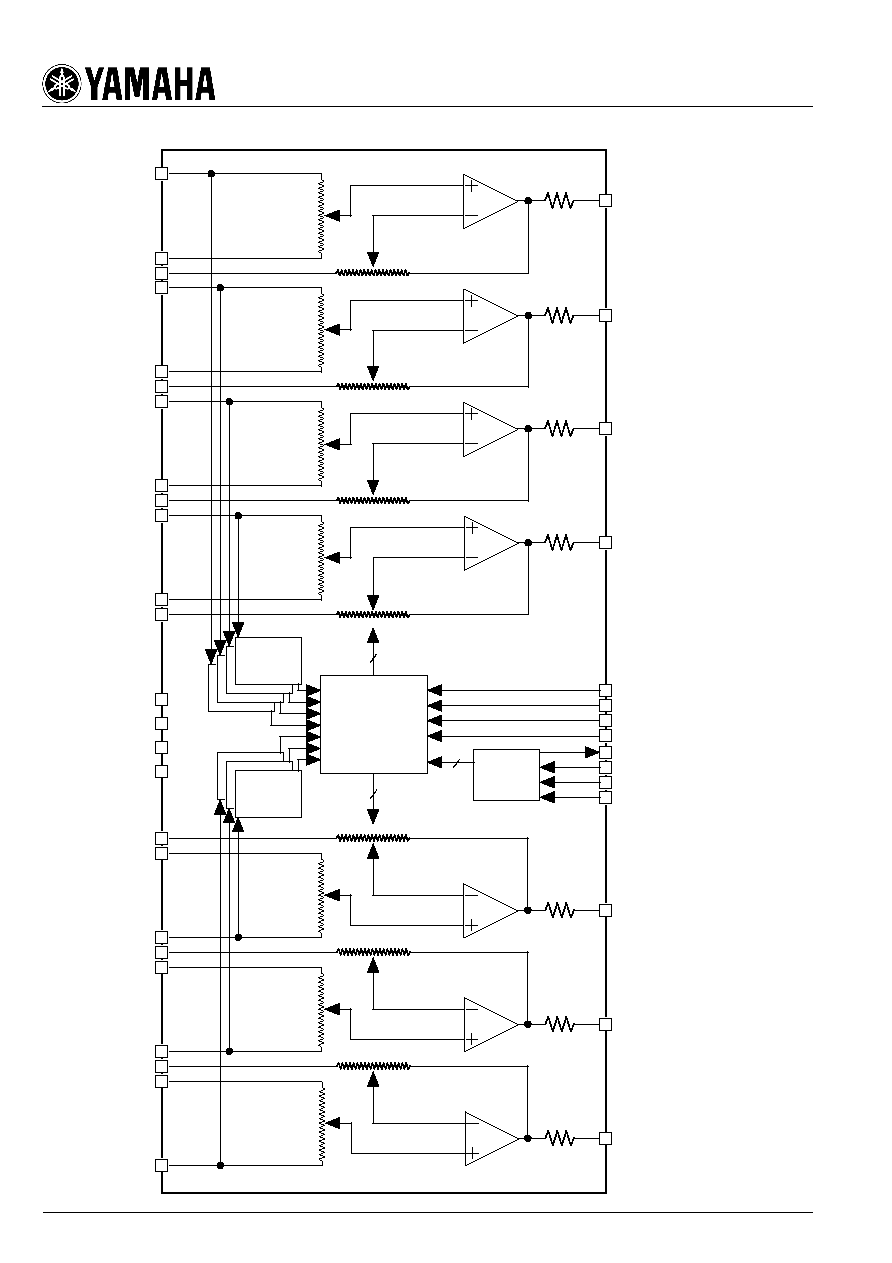
ch1 analog input
ch2 analog input
ch3 analog input
ch4 analog input
ch5 analog input
ch6 analog input
ch7 analog input
ch7 analog reference voltage input 7B Connect to ground directly.
Non connection or connect to ground.
ch5 analog output
ch1 analog output
Non connection or connect to ground.
ch4 analog output
Minus power supply for analog (-6.0V Typ.)
ch7 analog output
ch6 analog output
ch3 analog output
ch2 analog output
Non connection or connect to ground.
Non connection or connect to ground.
Minus power supply for analog (-6.0V Typ.)
Zero-cross control input 1. Select one from four types of zero-cross modes including non-zero-
Chip select input
Serial data input
Serial clock input
Test terminal Non connection or connect to DGND terminal.
Digital ground
-
-
-
-
Note A: analog terminal, OD: Open drain output terminal, "L" level means V
IL
, "H" level means V
IH
.
AVDD
-
-
Plus power supply for analog (+6.0V Typ.)
Minus power supply for analog (-6.0V Typ.)
AI
AI
AI
AI
AI
AI
AI
AI
AI
AI
AI
AI
AI
AI
ch7 analog reference voltage input 7A
Connect to ground through 33 F.
ch6
analog reference voltage input 6B Connect to ground directly.
ch6
analog reference voltage input 6A
Connect to ground through 33 F.
ch5
analog reference voltage input 5B Connect to ground directly.
ch5
analog reference voltage input 5A
Connect to ground through 33 F.
ch4
analog reference voltage input 4A
Connect to ground through 33 F.
ch4
analog reference voltage input 4B Connect to ground directly.
ch3
analog reference voltage input 3A
Connect to ground through 33 F.
ch3
analog reference voltage input 3B Connect to ground directly.
ch2
analog reference voltage input 2A
Connect to ground through 33 F.
ch2
analog reference voltage input 2B Connect to ground directly.
ch1
analog reference voltage input 1A
Connect to ground through 33 F.
ch1
analog reference voltage input 1B Connect to ground directly.
-
AO
AO
-
-
TE1
45
I Test terminal Non connection or connect to DGND terminal.
-
changes at 1 second or more after the rise of CSN signal.
cross mode. When changing zero-cross modes during operation, set the system so that it
Zero-cross control input 2. Select one from four types of zero-cross modes including non-zero-
changes at 1 second or more after the rise of CSN signal.
cross mode. When changing zero-cross modes during operation, set the system so that it
Serial
data
output
Serial data are outputted from this terminal when CSN pin is "L" level. This terminal becomes
high-impedance state when CSN pin is "H". Since it is an open drain output pin, pull it up
connected. Do not allow output current of 1.5mA or over.
through a resistor to the power supply voltage (to be AVDD or less) of a device to be
Reference voltage output for digital For attaining stabilization, connect this terminal to
AVSS terminal through a capacitance of 10µF or higher (C
REF
).
When avoid the use of this terminal, connect to ground.
And please use the output impedance of the source of input
signal less than 2.2k .
And please do not use this terminal output for the drive purpose of an external circuit.

YAC523
5
Description of functions
Analog functions
Maximum input voltage
The maximum amplitude of the input signal that is inputted to the analog input pin of YAC523 is 4.2Vrms when
power supply voltage is ±6V.
For a system to which a signal exceeding the power supply voltage (AVDD/AVSS) may be applied, use external
diodes to suppress the signal to the maximum rating or less.
Maximum output voltage
The maximum output voltage(THD<1
) of the signal that is outputted from the analog output pin of YAC523 is
4.2Vrms when power supply voltage is ±6V and no load is connected. The output impedance is 100
(typ.).
Realization of low residual noise system
General audio amplifiers are designed to have input sensitivity of approximately 150mV, and have a gain of
approximately 16dB at the preamplifier (PreAMP) section and approximately 30dB at the main amplifier section
(MainAMP).
The residual noise of YAC523 (Gain=-) is 1.2 Vrms (typ.) which is very small, and the device has positive side
gain (max: 31.5dB). Therefore, by using YAC523 also as "PreAMP", systems with a very small residual noise
and amplification of volume control noise can be configured.
For conventional configurations that need a "PreAMP", even if the residual noise of the volume control itself is
zero, the noise that is produced at the "PreAMP" is amplified by the gain, the noise becomes very high when it is
heard at the speakers.
When the input converted noise of "PreAMP" is 1 V, the conventional configuration produces noise of
approximately 200
V at the speakers. For the configuration that uses YAC523, the noise is 38 V which is very
small.
1Vrms
6.3Vrms
200Vrms
Volume
PreAMP
MainAMP
+16dB
+30dB
Residual noise produced by
conventional configuration
Residual noise produced by a
configuration that adopts YAC523
YAC523
1.2Vrms
38Vrms
Volume + PreAMP
MainAMP
-+16dB
+30dB
Zin=50k