 | –≠–ª–µ–∫—Ç—Ä–æ–Ω–Ω—ã–π –∫–æ–º–ø–æ–Ω–µ–Ω—Ç: YSS901-E | –°–∫–∞—á–∞—Ç—å:  PDF PDF  ZIP ZIP |

YAMAHA CORPORATION
YSS901CATALOG
CATALOG No.: LSI-4SS901A0
1999. 1
YSS901
SD
Preliminary
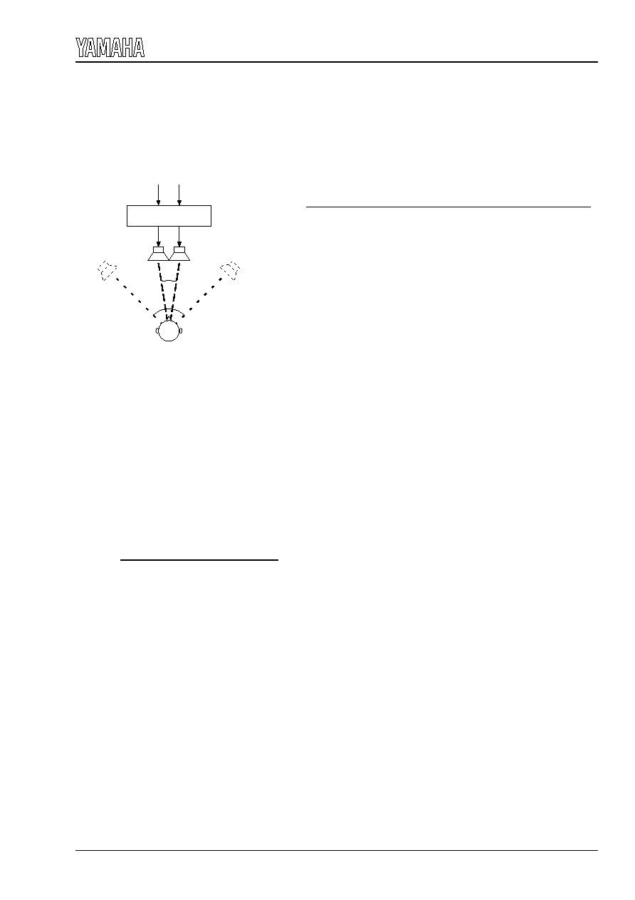
Stereo dipole
g Outline
YSS901 is a device that uses the stereo dipole system (SD) with which the transaural system can be constructed.
When a stereophonic signal that has been processed with the SD system of this device is inputted to two
speakers located adjacently at the center of the field (or to two speakers contained in one cabinet), the virtual
sound positioning function of this system produces the stereophonic sound similar to the one that can be
obtained by using an ordinary stereophonic sound replay system through the central two speakers.
YSS901 has built-in one bit Delta-Sigma type A/D and D/A converters for each of the two channels at its input
and output respectively. Thanks to these built-in converters, this device can process analog stereophonic sound
signal through the converters in addition to digital stereophonic sound signal.
This device performs an advanced convolution through DSP using the FIR filter.
g Features
n
Two channel virtual sound positioning by using the stereo dipole system.
n
Processes analog or digital signals at each of the two channels.
n
Four types of digital data format are available, including 48 fs Serial-DAC16, 18 and 20 bits, and 64 fs.
n
Six types of parameter coefficients are built in the device. Additional parameter coefficients can be
downloaded externally.
n
The parameter control is made through the DC switches or synchronous three-wire serial system.
n
Uses a clock of 2.822 MHz from the crystal. External clock can also be used.
n
Has a built-in PLL circuit for generating clock for operation.
n
Internal operating frequency of 512 fs.
n
Allows fading in or out the output of the results of the convolution when switching the coefficient.
n
Power supply voltage: 5 V
n
Si-gate CMOS process.
n
64 QFP
YSS901
2
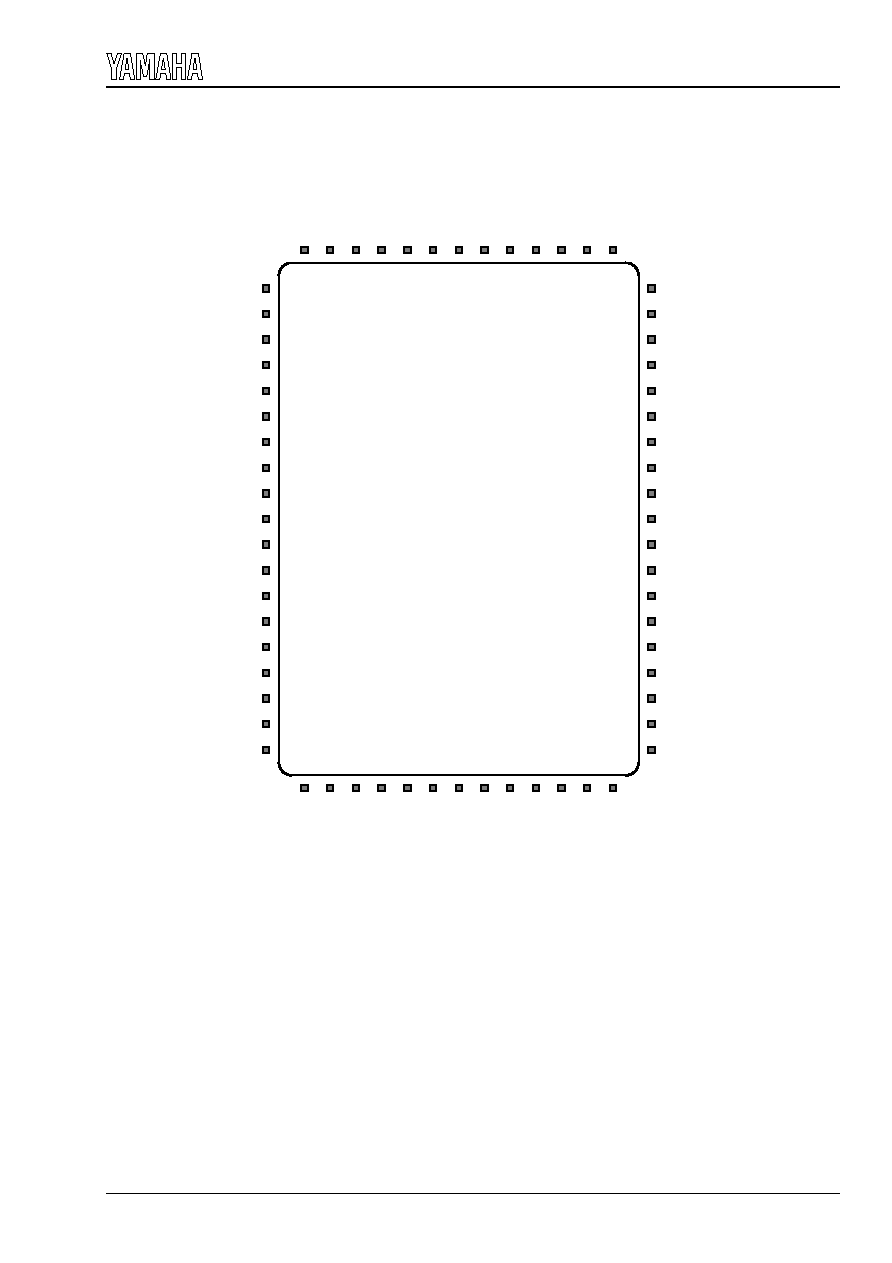
g Pin configuration
<64QFP TOP VIEW>
YSS901
123456789
1
0
1
1
63
23
24
25
26
27
28
29
30
20
21
61
22
34
35
36
37
38
39
40
41
42
62
43
33
53
54
55
56
57
58
59
60
TSTNI
AILRET
AIR
LOUT
ROUT
TSTNO
AVDD
DSEL2
AVSS
AVSS
DIN
DOUT
BCLK
DSEL1
DSEL0
SYNCN
CTLSEL
CSEL1
BSFT0
CSN
SCK
SI
RESETN
XTAL
TST2
TSTSEL
DVSS
TSTCK
PLLC
DVSS
EXTAL
AIL
AIRRET
AILOUT
AIROUT
DVSS
DVDD
VREF
CSEL0
CSEL2
BSFT1
DVDD
DVDD
TST1
12
13
14
15
16
17
18
19
31
32
44
45
46
47
48
49
50
51
52
64
N.C
N.C
N.C
N.C
N.C
N.C
N.C
N.C
N.C
N.C
N.C
N.C
N.C
N.C
N.C
N.C
N.C
N.C
N.C
N.C
YSS901
3
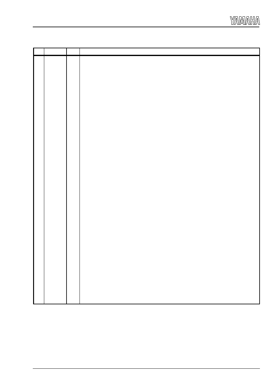
g Pin Description
No.
Pin name
I/O
Function
5
DVDD
-
Digital signal power supply : +5 V
6
CTLSEL
I
Selection of control method
7
SYNCN
I
Digital input/output synchronization signal
8
BCLK
I
Digital input/output bit clock
9
CSN
I
Serial control interface chip select signal
10
DOUT
O
Digital signal output
11
DIN
I
Digital signal input
12
DSEL2
I
Analog/digital input selection
13
DSEL1
I
Digital input/output format selection
14
DSEL0
I
Digital input/output format selection
15
DVDD
-
Digital signal power supply : +5 V
21
TST2
-
Test (To be open.)
22
DVSS
-
Digital signal ground
23
AVSS
-
Analog signal ground
24
AIRRET
AO
Right channel analog signal input return
25
AIROUT
AO
Right channel analog signal input out
26
AIR
AI
Right channel analog signal input
27
AILRET
AO
Left channel analog signal input return
28
AILOUT
AO
Left channel analog signal input out
29
AIL
AI
Left channel analog signal input
30
VREF
AI
Analog signal VREF
31
AVDD
-
Analog signal power supply : +5 V
37
LOUT
AO
Left channel analog signal output
38
ROUT
AO
Right channel analog signal output
39
PLLC
AI
PLL auxiliary input
40
AVSS
-
Analog signal ground
41
EXTAL
I
Crystal clock input
42
XTAL
O
Crystal clock output
43
DVSS
-
Digital signal ground
44
TSTCK
-
Test (Connect with DVSS.)
45
TST1
-
Test (To be open.)
46
TSTNI
I
Test (Connect with DVSS.)
47
TSTNO
O
Test (To be open.)
53
DVDD
-
Digital signal power supply: +5 V
54
TSTSEL
-
Test (Connect with DVSS.)
55
CSEL2
I
Coefficient selection (Enabled when CTLSEL = 0)
56
CSEL1
I
Coefficient selection (Enabled when CTLSEL = 0)
57
CSEL0
I
Coefficient selection (Enabled when CTLSEL = 0)
58
RESETN
I
Reset signal input
59
BSFT1
I
Bit shift selection (Enabled when CTLSEL = 0)
60
BSFT0
I
Bit shift selection (Enabled when CTLSEL = 0)
61
SCK
I
Serial control interface clock input
62
SI
I
Serial control interface data input
63
DVSS
-
Digital signal ground
Notes:
1. Pins of No. 1 to 4, 16 to 20, 32 to 36, 48 to 52 and 64 are to be open.
2.
I: input pin
O: output pin
AI: analog signal input pin
AO: analog output pin.
YSS901
4
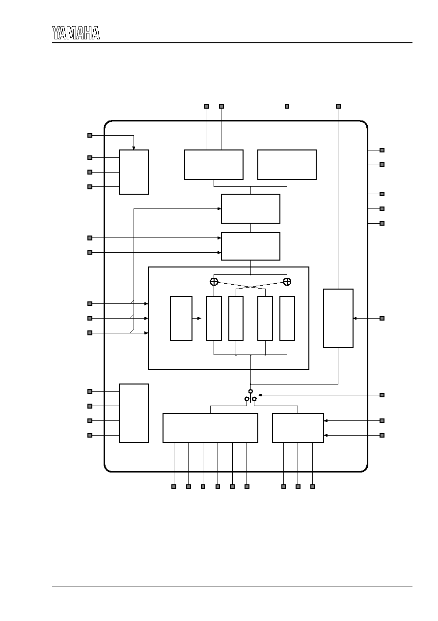
g Block Diagram
NGATE
AILRET
AIR
AIL
AIRRET
AILOUT
AIROUT
AD
DA
Digital
In
Digital
Out
Noise Gate
Serial
Control
COEF
stereo dipole
Timing
Fader
SYNCN
BCLK
DIN
ROUT
LOUT
DOUT
PLLC
EXTAL
XTAL
RESETN
CSEL0
CSEL1
CSEL2
BSFT0
BSFT1
CSN
SCK
SI
CTLSEL
Lch
Lch
Rch
Rch
COEF 1
COEF 2
COEF 1
COEF 2
DSEL1
DSEL0
Bit
Shift
DSEL2
NGO
AVSS
AVDD
VREF
DVDD
DVSS
Lch
Rch
(Input Level Check)

YSS901
5
g Outline of Functions
1.
Clock signals
XTAL, EXTAL
and
PLLC
For the clock signal, use the crystal connected to XTAL EXTAL pin with which the clock signal is obtained by the
self-oscillation at the crystal oscillation circuit, or external signal supplied through EXTAL pin. The frequency of the
clock obtained by the self-oscillation is 2.822 MHz (or 44.1 kHz * 64). The internal operation is carried out with 512
fs clock that is made by the PLL.
Insert an analog filter in between PLLC and GND pins.
2. Data input/output signals
Analog/digital input selection pin:
DSEL2
This pin is used to select a type of the input signal. DSEL2 = 0 selects the digital signal input, or DSEL2 = 1 selects
the analog signal input.
2-1) Digital signal
Digital signal input/output pins:
DIN, BCLK, SYNCN
and
DOUT
Digital signals should be inputted through DIN, BCLK and SYNCN pins.
DIN signal (PCM data) must be in synchronous with BCLK (bit clock) and SYNCN (word clock) signals.
Digital signal is outputted from DOUT pin.
Input/output format designation pins:
DSEL1
and
DSEL0
These pins are used to designate a data format for DAC. The settings of DSEL1 and DSEL0 and their output formats
are as follows.
DSEL1 DSEL0
DAC output format
0
0
48 fs 16 bits Data LSB justified
0
1
48 fs 18 bits Data LSB justified (Bits 1 and 0 are "0".)
1
0
48 fs 20 bits Data LSB justified (Bits 3 through 0 are "0".)
1
1
64 fs 16 bits Data MSB justified (Delay by one bit)
For the details of the format, refer to "Serial Data Interface" explained later in this document.
2-2) Analog signal
Analog input/output pins:
AIL, AILOUT, AILRET, LOUT, AIR, AIROUT, AIRRET
and
ROUT
Analog signals should be inputted through AIL and AIR pins. The signals that have been processed by the stereo
dipole (SD) are outputted from LOUT and ROUT pins respectively. Add an analog filter circuit, an example of
which is shown later in this document.
Center voltage pin
VREF
This pin outputs a reference voltage for analog signal processing. Connect an appropriate capacitor between VREF
and GND pins.
3. Controlling functions
3-1) Control method selection pin:
CTLSEL
This pin is used for selection of a control method as described below.
CTLSEL = 0 : Selection of CSEL2, CSEL1 or CSEL0 by means of DC switch (H/L) is enabled.
CTLSEL = 1 : Selection of CSN, SI or SCK through the microcomputer is enabled.
YSS901
6
3-2) Speaker arrangement angle and virtual sound position angle
3-2-1) Setting by means of DC switches:
CSEL2, CSEL1, CSEL0
and
CTLSEL
By setting CTLSEL to "0", and setting CSEL 2, 1 and 0 as following, the positioning angle between the front two
speakers and the virtual sound positioning angle can be selected.
stereo dipole
Stereo Input
Real Source
Virtual Source
Listener
L
R
L
R
a
b
Speaker positioning Virtual
CSEL2 CSEL1 CSEL0 angle (a) sound position (b)
0 0 0 10 degrees 60 degrees
0 0 1 10 degrees 120 degrees
0 1 0 15 degrees 60 degrees
0 1 1 15 degrees 120 degrees
1 0 0 20 degrees 60 degrees
1 0 1 20 degrees 120 degrees
1 1 0 External coefficien1t downloadable
1 1 1 Through (SD effect is disabled.)
* Your original coefficients can be written by an external microprocessor.
(Technical material is under preparation)
3-2-2) Control through CPU
CSN, SCK, SI
and
CTLSEL
Data can be written into the control registers through the serial microcomputer interface by using three pins including
CSN, SCK and SI.
For the details of the read/write timing, refer to the format diagram shown in the next page.
3-3) Bit shift
BSFT1, BSFT0
and
CTLSEL
This function is used to specify the amount of bit shift after the addition of the results of filtering.
CTLSEL = 0 enables the settings of BSF1 and BSF0.
The relation between the combinations of settings of BSF1 and BSF0 and the amount of bit shift is as shown below.
BSFT1 BSFT 0 Bit shift
0
0
None
0
1
-1 bit
1
0
-2 bit
1
1
-3 bit
CTLSEL = 1 enables the control of bit shift amount through the microcomputer interface.
4. Initial clear
RESETN
This LSI requires an initial clear at power on moment.
5. LSI test pins
TST1, TST2, TSTCK, TSTSEL, TSTNI
and
TSTNO
TST1, TST2 and TST0 are to be open. TSTCK, TSTSEL and TSTNI should be connected with DVSS.
YSS901
7
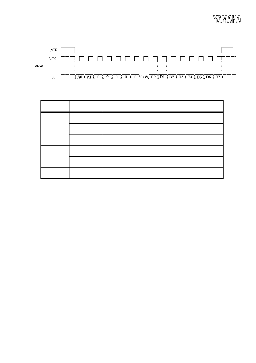
g Serial Microcomputer Interface
Format for writing data through microcomputer
After setting the address (A0 and A1) through SI, it is possible to write data (D0 to D7) into the specified address
when R/W bit has been set to "0". The address map is as shown below.
Address
Data
Description
A1, A0
0 0
D0
CSEL0
D1
CSEL1
D2
CSEL2
D3
BSFT0
D4
BSFT1
D5 to D7
To be "0".
0 1
D0
Write address selection
D1
Write address counter clear
D2
RAM clear
D3 to D7
To be "0".
1 0
D7 to D0
Coefficient data to be written (higher byte)
1 1
D7 to D0
Coefficient data to be written (lower byte)
How to write coefficient data into RAM
Two coefficients are used as a set, each constituted with 16 bits x 125 taps.
The first coefficient ("coef1" shown in the block diagram) is written into RAM address 0-124, and the second one
("coef2" shown in the block diagram) into RAM address 125-249.
The address counter for writing the data uses seven (7) bits, the upper bit (8th bit) uses "write address selection" of
D2 with A1, A0 = 0 1.
Data writing procedure
(1) Clear the RAM and write address counter. (RAM clear needs up to 2 fs to be completed.)
(2) When the RAM has been cleared, write data into higher byte and then into lower byte starting at the first
byte of the first coefficient. (When the writing into the lower byte has been completed, the data is actually
written into RAM. Wait 1 fs before writing the data into higher byte of the next coefficient.)
(3) When the first coefficient has been written, write the second one by using the same procedure. Set the
"write address selection" bit to "1" when writing data into the 4th tap and after of the second coefficient.

YSS901
8
g Serial Data Interface
Timing of the serial data interface as shown below
00
00
01
02
03
02
03
00
00
01
00
01
02
03
04
05
06
07
08
09
10
11
12
13
14
15
BCLK
SYNCN
DIN,DOUT
(1) Dac 48fs 16bit format
(2) Dac 48fs 18bit format
(3) Dac 48fs 20bit format
(4) 64fs YAMAHA-DSP format
00
01
02
03
04
05
06
07
08
09
10
11
12
13
14
15
02
03
04
05
06
07
08
09
10
11
12
13
14
15
BCLK
SYNCN
DIN,DOUT
02
03
04
05
06
07
08
09
10
11
12
13
14
15
16
17
16
17
04
05
06
07
08
09
10
11
12
13
14
15
BCLK
SYNCN
DIN,DOUT
04
05
06
07
08
09
10
11
12
13
14
15
16
17
16
17
18
19
18
19
00
01
02
03
04
05
06
07
08
09
10
11
12
13
14
15
00
01
02
03
04
05
06
07
08
09
10
11
12
13
14
15
01
01
00
01
02
00
02
01
17
18
19
00
02
01
10
11
12
13
14
15
BCLK
SYNCN
DIN,DOUT

YSS901
9
g Electrical Characteristics
1. Absolute Maximum Rating
Items
Symbol
Min.
Max.
Unit
Power supply Voltage
VDD
Vss-0.5
Vss+7.0
V
Input Voltage
VI
Vss-0.5
VDD1+0.5
V
Input Current
II
-20
+20
mA
Storage Temperature
Tstg
-50
125
C
2. Recommended Operating Conditions
Items
Symbol
Min.
Typ.
Max.
Unit
Power supply Voltage
VDD
4.75
5.0
5.25
V
Operating Temperature
Top
0
25
70
C
3. DC Characteristics (Condition: Under Recommended Operating Conditions)
Items
Symbol
Condition
Min.
Typ.
Max.
Unit
Input Voltage H level
VIH2 *1
2.2
V
Input Voltage L level
VIL2 *1
0.8
V
Output Voltage H level
VOH IOH = -80
mA *2
VDD1-1.0
V
Output Voltage L level
VOL
IOL = 1.6 mA *2
0.4
V
Output Capacitance
CO
*2
50
pF
Power Consumption
PD
500
mW
*1 Applicable to input terminals other than analog terminals
*2 Applicable to output terminals other than analog terminals

YSS901
10
4. AC Characteristics (Condition: Under Recommended Operating Conditions)
Items
Symbol
Condition
Min.
Typ.
Max.
Unit
XI Clock
Frequency
Xin
2.822
MHz
Duty
Xduty
40
50
60
%
SCK,SI,CSN
Set up time
Hold Time
Tset
Thold
40
40
-
-
-
-
ns
ns
BCLK,SYNCN,DIN,DOUT
Set up time
Hold time
Output Delay time
Tset
Thold
Td
40
40
-
-
-
-
-
-
40
ns
ns
ns
SCK
SI,CSN
Tset
Thold
BCLK
DIN,SYNCN
DOUT
Tset
Thold
Td
BCLK
DIN,SYNCN
DOUT
Tset
Thold
Td

YSS901
11
g Design Example
The figure below shows basic design example that uses YSS901.
Lin
Rin
Analog I/O
Lout
Rout
Digital I/O
Control
XTAL
DC Switch
OR
Serial Ctl
(from CPU)
10
1k
100k
100k
1
1.8k
1000p
8.2k
10k
220
220
560
10k
470p
1M
680
22p
22p
2.8224M
10/16
0.1
YSS901
123456789
1
0
1
1
63
23
24
25
26
27
28
29
30
20
21
61
22
34
35
36
37
38
39
40
41
42
62
43
33
53
54
55
56
57
58
59
60
TSTNI
AILRET
AIR
LOUT
ROUT
TSTNO
AVDD
DSEL2
AVSS
AVSS
DIN
DOUT
BCLK
DSEL1
DSEL0
SYNCN
CTLSEL
CSEL1
BSFT0
CSN
SCK
SI
RESETN
XTAL
TST2
TSTSEL
DVSS
TSTCK
PLLC
DVSS
EXTAL
AIL
AIRRET
AILOUT
AIROUT
DVSS
DVDD
VREF
CSEL0
CSEL2
BSFT1
DVDD
DVDD
TST1
12
13
14
15
16
17
18
19
31
32
44
45
46
47
48
49
50
51
52
64
N.C
N.C
N.C
N.C
N.C
N.C
N.C
N.C
N.C
N.C
N.C
N.C
N.C
N.C
N.C
N.C
N.C
N.C
N.C
N.C

YSS901
12
g
External Dimensions
C-PK64FP-1
(UNIT) : mm (millimeters)
The figure in the parenthesis ( )
should be used as a reference.
Plastic body dimensions do not
include burr of resin.
UNIT: mm
1
19
0.15 +/- 0.05
(LEAD THICKNESS)
2.95 MAX.
0 MIN.
(STAND OFF)
0-15 deg.
1.20 +/- 0.20
(2.40)
51
33
24.80 +/- 0.40
14.00
+/- 0.30
P-1.00TYP
or 0.40 +/- 0.10
20.00 +/- 0.30
18.80
+/- 0.40
32
20
64
52
0.35 +/- 0.10

YSS901
13
Memo

YSS901
Yamaha reserves the right to make changes to its Products and to this document
without notice. The information contained in this document has been carefully checked
and is believed to be reliable. However, Yamaha assumes no responsibilities for
inaccuracies and makes no commitment to update or to keep current the information
contained in this document.
These Yamaha Products are designed only for commercial and normal industrial
applications, and are not suitable for other uses, such as medical life support
equipment, nuclear facilities, critical care equipment or any other application the failure
of which could lead to death, personal injury or environmental or property damage. Use
of the Products in any such application is at the customer's sole risk and expense.
Yamaha assumes no liability for incidental , consequential, or special damages or injury
that may result from misapplication or improper use or operation of the Products.
Yamaha makes no warranty or representation that the Products are subject to
intellectual property license from Yamaha or any third party, and Yamaha makes no
warranty excludes any liability to the Customer or any third party arising from or related
to the Products' infringement of any third party's intellectual property rights, including
the patent, copyright, trademark or trade secret rights of any third party.
Examples of use described herein are merely to indicate the characteristics and
performance of Yamaha products. Yamaha assumes no responsibility for any intellectual
property claims or other problems that may result from applications based on the
examples described herein. Yamaha makes no warranty with respect to the products,
express or implied, including, but not limited to the warranties of merchantability, fitness
for a particular use and title.
1.
2.
3.
4.
5.
IMPORTANT NOTICE
The specifications of this product are subject to improvement changes without prior notice.
AGENCY
All rights reserved
©
1999
Address inquiries to:
Semiconductor Sales & Marketing Department
Head Office
203, Matsunokijima, Toyooka-mura
Iwata-gun, Shizuoka-ken, 438-0192
Electronic Equipment Business section
Tel. 81-539-62-4918
Fax. 81-539-62-5054
Tokyo Office
2-17-11, Takanawa, Minato-ku,
Tokyo, 108-8568
Tel. 81-3-5488-5431
Fax. 81-3-5488-5088
Osaka Office
Namba Tsujimoto Nissei Bldg, 4F
1
-13-17, Namba Naka, Naniwa-ku,
Osaka City, Osaka, 556-0011
Tel. 81-6-6633-3690
Fax. 81-6-6633-3691
U.S.A. Office
YAMAHA Systems Technology.
100 Century Center Court, San Jose, CA95112
Tel. 1-408-467-2300
Fax. 1-408-437-8791