 | –≠–ª–µ–∫—Ç—Ä–æ–Ω–Ω—ã–π –∫–æ–º–ø–æ–Ω–µ–Ω—Ç: YSS922-S | –°–∫–∞—á–∞—Ç—å:  PDF PDF  ZIP ZIP |
YAMAHA CORPORATION
YSS922 CATALOG
CATALOG No.: LSI-4SS922A1
2000.2
YSS922
AC3D3
96kHz DIR + Dolby Digital / Pro Logic / DTS decoder + Sub DSP
OUTLINE
YSS922 is one chip LSI consisting of three built-in blocks : Dolby Digital (AC-3) / Pro Logic & DTS decoder
(Main DSP), a programmable sound processing DSP (Sub DSP) and SPDIF receiver (DIR) which can handle up to
96kHz sampling frequency. The Sub DSP is capable of realizing various sound fields, such as virtual surround by
down-loading the program and coefficient from outside.
FEATURES
DIR Block
∑ Sampling frequency: two ranges are available including;
32k to 48kHz (normal rate) and
64k to 96kHz (double rate)
∑ Provides master clock, 256fs, to DAC, ADC and other peripheral devices. The clock output can be controlled
with various modes determined by register setting.
∑ Has a pin that indicates the double rate operation.
∑ Every channel status and user data can be read through the microprocessor interface.
∑ Has an output pin for interrupt that is activated by changing of the status information.
∑ Internal operation frequency: 25MHz
Main DSP Block
∑ Dolby Digital (AC-3) / Pro Logic and DTS decode
∑ High quality internal 24 bit DSP
∑ No external memory is required. (Memory for center and surround channel delay is included.)
∑ AC-3 Karaoke mode.
∑ Supports compression modes at AC-3 / DTS decoding.
∑ Pro Logic decoding for Dolby Digital 2 channels decoded signal as well as ordinary PCM signal.
∑ Reads Dolby Digital / DTS decode information through the microprocessor interface.
∑ Included de-emphasis filter for the PCM signal.
∑ Internal operation frequency: 30MHz
Preliminary

YSS922
2
Sub DSP Block
∑ Capable of realizing various sound fields, such as simulation surround, output configuration and virtual surround
by down-loading the programs.
∑ Adoption of the 32 bit floating point DSP assuring highly accurate processing.
∑ Up to 2.73 seconds delay at fs=48kHz achievable by adding DRAM or SRAM externally.
∑ Internal operation frequency: 30MHz
Other Features
∑ Connectable to almost all ADC and DAC by making appropriate settings to the control register.
∑ Total of 16 general purpose input/output ports are available.
∑ 2 built-in PLL circuits for generation of operation clocks for DIR block and DSP blocks.
∑ Supports the power down mode.
∑ Power supply voltage: 2 power sources (2.5V for core logic section and 3.3v for I/O section)
∑ Si-gate CMOS process
∑ 128SQFP (YSS922-S)
Note: "AC-3" and "Pro Logic" are registered trademarks of Dolby Laboratories Licensing corporation.
"DTS" is a registered trademark of DTS, Inc.
Use of this LSI must be licensed by both Dolby Laboratories Licensing Corporation and DTS, Inc.

YSS922
3
BLOCK DIAGRAM
D I R M C K
DDIN0
DDIN1
DDIN2
DDIN3
D D I N S E L
V
ERR/BS
DBL/V
DIRINT
P L L
D I R
DIRO Interface
D I R B C K
D I R W C K
S D I A S E L
SDIA Interface
S D I A C K S E L
S D W C K I 0
S D B C K I 0
/ S D B C K O
C R C
D I R P C O
D I R S D O
S D I A
S U R E N C
K A R A O K E
M U T E
C R C
A C 3 D A T A
D T S D A T A
N O N P C M
Z E R O F L G
X I
X O
C P O
P L L
C l o c k f o r D I R
B l o c k ( 2 5 M H z )
C l o c k f o r D S P
B l o c k ( 3 0 M H z )
S D O A I n t e r f a c e
M a i n D S P
( A C - 3 / P r o L o g i c / D T S d e c o d e r )
SDIB Interface
S D O A 0
S D O A 1
S D O A 2
L , R
L S , R S
C , L F E
S D I B 0
S D I B 1
S D I B 2
S D I B 3
S D I B S E L
SDIBCKSEL
External Memory
Interface
S u b D S P
R A M D 0 - 1 5
C A S N
R A S N
R A M W E N
R A M O E N
R A M A 0 - 1 7
O V F B / E N D
S D O B I n t e r f a c e
SDOBCKSEL
SDOB3
SDOB2
SDOB1
SDOB0
SDWCKI1
SDBCKI1
O P O R T 0 - 7
Coefficient /
P r o g r a m R A M
MPLOAD
/ C S
S O
SI
S C K
I P O R T 0 - 4
Control Signal
D B L
Control Register
Microprocessor I/F
V M O D
B S M O D
ERR
BS
SYNC
U
FS128
C
SYNC/U
FS128/C
U M O D
C M O D
OVFSEL
O V F B
E N D
7
6
5
I P O R T 5 - 7
D I R P R O
/LOCK
YSS922
4
PIN CONFIGRATION
< 1 2 8 S Q F P T O P V IE W >
SDBCK
I1
R A M D 8
OP
O
R
T1
OP
O
R
T2
OP
O
R
T4
OP
O
R
T3
OP
O
R
T6
OP
O
R
T5
R A M D 0
OP
O
R
T7
R A M D 1
R A M A 6
V D D 2
R A M O E N
R A M A 0
V S S
V D D 1
R A M W E N
R A S N
R A M D 1 5
C A S N
R A M D 1 3
R A M D 1 4
R A M A 7
V S S
R A M D 1 1
R A M D 1 2
V D D 1
R A M D 1 0
R A M D 7
V S S
R A M D 5
R A M D 6
R A M D 3
R A M D 4
SD
O
B
3
R A M D 2
SD
O
B
2
R A M A 8
VS
S
DBL
/
V
SD
WCK
I
1
SY
N
C
/U
FS128/C
ERR/BS
R A M D 9
DI
RBCK
DI
RMCK
DI
RWCK
/S D B C K O
OP
O
R
T0
DI
RS
DO
SD
O
B
0
VD
D1
SD
O
B
1
R A M A 1 1
R A M A 2
R A M A 4
R A M A 1
R A M A 5
R A M A 9
R A M A 1 0
VS
S
R A M A 3
VS
S
SCK
/IC
SO
SI
/LO
CK
/CS
MU
TE
CRC
DT
S
D
A
T
A
SU
RE
N
C
VS
S
NO
NP
CM
ZE
ROFL
G
DI
RIN
T
RA
MA1
7
OV
FB/END
RA
MA1
5
RA
MA1
6
RA
MA1
3
RA
MA1
4
VD
D2
RA
MA1
2
D D IN 3
T E S T X I
T E S T B R K
A V S S
T E S T R 2
T E S T R 1
V D D 2
X O
D D IN 0
X I
D D IN 2
D D IN 1
S D B C K I0
D IR P R O
V S S
S D W C K I0
A V D D
C P O
V D D 1
D IR P C O
IP O R T 1
IP O R T 0
IP O R T 3
IP O R T 2
T E S T X O
IP O R T 4
T E S T X E N
T E S T M S
V S S
VD
D2
VD
D1
AC
3D
AT
A
KA
R
A
O
K
E
S D O A 2
S D IA
S D O A 0
S D O A 1
S D IB 2
S D IB 3
S D IB 0
S D IB 1
1 0 1
1 0 2
9 9
1 0 0
9 7
9 8
9 5
9 6
9 3
9 4
9 1
9 2
8 9
9 0
8 7
8 8
8 5
8 6
8 3
8 4
8 1
8 2
7 9
8 0
7 7
7 8
7 5
7 6
7 3
7 4
7 1
7 2
6 9
7 0
6 7
6 8
6 5
6 6
128
127
125
126
123
124
121
122
119
120
117
118
115
116
113
114
111
112
109
110
107
108
105
106
103
104
2
1
4
3
6
5
8
7
1 0
9
1 2
1 1
1 4
1 3
1 6
1 5
1 8
1 7
2 0
1 9
2 2
2 1
2 4
2 3
2 6
2 5
2 8
2 7
3 0
2 9
3 2
3 1
3 4
3 3
3 6
3 5
3 8
3 7
63
61
62
59
60
57
58
55
56
53
54
51
52
49
50
47
48
45
46
43
44
41
42
39
40
64

YSS922
5
PIN FUNCTION
No.
Name
I/O
Function
1
TESTXI
I
LSI Test Pin (must be connected to VSS)
2
TESTXO
O
LSI Test Pin (to be open)
3
VDD2
-
+2.5V Power Supply (for Internal Core Logic)
4
XO
O
Crystal oscillator connection
5
XI
I
Crystal oscillator connection (24.576MHz)
6
TESTMS
I+
LSI Test Pin (to be open)
7
TESTXEN
I+
LSI Test Pin (to be open)
8
IPORT0
I+
General purpose input port
9
IPORT1
I+
General purpose input port
10
IPORT2
I+
General purpose input port
11
IPORT3
I+
General purpose input port
12
IPORT4
I+
General purpose input port
13
DDIN0
Is
DIR: Digital audio interface data input 0
14
DDIN1
Is
DIR: Digital audio interface data input 1 / General purpose input port
15
DDIN2
Is
DIR: Digital audio interface data input 2 / General purpose input port
16
DDIN3
Is
DIR: Digital audio interface data input 3 / General purpose input port
17
VSS
-
Ground
18
CPO
A
PLL filter connection
19
AVDD
-
+3.3V Power Supply (for DIR block)
20
DIRPCO
A
DIR: PLL filter connection
21
DIRPRO
A
DIR: PLL filter connection
22
AVSS
-
Ground (for DIR block)
23
TESTBRK
I+
LSI Test Pin (to be open)
24
TESTR1
I+
LSI Test Pin (to be open)
25
TESTR2
I+
LSI Test Pin (to be open)
26
VDD1
-
+3.3V Power Supply (for I/O)
27
SDWCKI0
I+
Word clock input for SDIA, SDOA, SDIB, SDOB
28
SDBCKI0
I+
Bit clock input for SDIA, SDOA, SDIB, SDOB
29
/SDBCKO
O
Reverse clock output of DIRBCK or SDBCKI0
30
SDIA
I
Input of bitstream or PCM data to Main DSP
31
SDOA2
O
PCM data output from Main DSP (C, LFE)
32
SDOA1
O
PCM data output from Main DSP (LS, RS)
33
SDOA0
O
PCM data output from Main DSP (L, R)
34
SDIB3
I+
PCM data input to Sub DSP
35
SDIB2
I+
PCM data input to Sub DSP
36
SDIB1
I+
PCM data input to Sub DSP
37
SDIB0
I+
PCM data input to Sub DSP
38
VSS
-
Ground
39
VDD2
-
+2.5V Power Supply (for Internal Core Logic)
40
DIRSDO
O
Output of bitstream or PCM data from DIR
41
DIRWCK
O
DIR: Serial data word clock (fs) output
42
DIRBCK
O
DIR: Serial data bit clock (64fs) output
43
DIRMCK
O
DIR: Serial data master clock (256fs or 128fs) output
44
ERR/BS
O
DIR: Data error detect / block start output
45
SYNC/U
O
DIR: Serial data synchronized timing / User data output
46
FS128/C
O
DIR: Serial data master clock 128fs / Channel status output
47
DBL/V
O
DIR: Double rate lock detect / Validity flag output
48
SDWCKI1
I+
Word clock input for SDIB, SDOB
49
SDBCKI1
I+
Bit clock input for SDIB, SDOB
50
VSS
-
Ground
51
SDOB3
O
PCM data output from Sub DSP
52
SDOB2
O
PCM data output from Sub DSP
53
SDOB1
O
PCM data output from Sub DSP
54
SDOB0
O
PCM data output from Sub DSP
55
VDD1
-
+3.3V Power Supply (for I/O)

YSS922
6
No.
Name
I/O
Function
56
OPORT0
O
General purpose output port
57
OPORT1
O
General purpose output port
58
OPORT2
O
General purpose output port
59
OPORT3
O
General purpose output port
60
OPORT4
O
General purpose output port
61
OPORT5
O
General purpose output port
62
OPORT6
O
General purpose output port
63
OPORT7
O
General purpose output port
64
VSS
-
Ground
65
VDD2
-
+2.5V Power Supply (for Internal Core Logic)
66
RAMD0
I+/O
Sub DSP: External memory interface Data 0
67
RAMD1
I+/O
Sub DSP: External memory interface Data 1
68
RAMD2
I+/O
Sub DSP: External memory interface Data 2
69
RAMD3
I+/O
Sub DSP: External memory interface Data 3
70
RAMD4
I+/O
Sub DSP: External memory interface Data 4
71
RAMD5
I+/O
Sub DSP: External memory interface Data 5
72
RAMD6
I+/O
Sub DSP: External memory interface Data 6
73
RAMD7
I+/O
Sub DSP: External memory interface Data 7
74
VSS
-
Ground
75
VDD1
-
+3.3V Power Supply (for I/O)
76
RAMD8
I+/O
Sub DSP: External memory interface Data 8
77
RAMD9
I+/O
Sub DSP: External memory interface Data 9
78
RAMD10
I+/O
Sub DSP: External memory interface Data 10
79
RAMD11
I+/O
Sub DSP: External memory interface Data 11
80
RAMD12
I+/O
Sub DSP: External memory interface Data 12
81
RAMD13
I+/O
Sub DSP: External memory interface Data 13
82
RAMD14
I+/O
Sub DSP: External memory interface Data 14
83
RAMD15
I+/O
Sub DSP: External memory interface Data 15
84
CASN
O
Sub DSP: External DRAM interface Column address strobe output
85
RAMWEN
O
Sub DSP: External memory interface Write enable output
86
RAMOEN
O
Sub DSP: External memory interface Output enable output
87
RASN
O
Sub DSP: External DRAM interface Row address strobe output
88
VSS
-
Ground
89
VDD1
-
+3.3V Power Supply (for I/O)
90
RAMA8
O
Sub DSP: External memory interface Address 8
91
RAMA7
O
Sub DSP: External memory interface Address 7
92
RAMA0
O
Sub DSP: External memory interface Address 0
93
RAMA6
O
Sub DSP: External memory interface Address 6
94
RAMA1
O
Sub DSP: External memory interface Address 1
95
RAMA5
O
Sub DSP: External memory interface Address 5
96
RAMA2
O
Sub DSP: External memory interface Address 2
97
RAMA4
O
Sub DSP: External memory interface Address 4
98
RAMA3
O
Sub DSP: External memory interface Address 3
99
RAMA9
O
Sub DSP: External memory interface Address 9
100
RAMA10
O
Sub DSP: External memory interface Address 10
101
RAMA11
O
Sub DSP: External memory interface Address 11
102
VSS
-
Ground
103
VDD2
-
+2.5V Power Supply (for Internal Core Logic)
104
RAMA12
O
Sub DSP: External memory interface Address 12
105
RAMA13
O
Sub DSP: External memory interface Address 13
106
RAMA14
O
Sub DSP: External memory interface Address 14
107
RAMA15
O
Sub DSP: External memory interface Address 15
108
RAMA16
O
Sub DSP: External memory interface Address 16
109
RAMA17
O
Sub DSP: External memory interface Address 17
110 OVFB/END
O
Sub DSP: Overflow / Program end detect

YSS922
7
No.
Name
I/O
Function
111
ZEROFLG
O
Main DSP: Zero flag output
112
VSS
-
Ground
113
NONPCM
O
Main DSP: non-PCM data detect
114
DTSDATA
O
Main DSP: DTS data detect
115
AC3DATA
O
Main DSP: AC-3 data detect
116
MUTE
O
Main DSP: Auto mute detect
117 KARAOKE
O
Main DSP: AC-3 Karaoke data detect
118
VDD1
-
+3.3V Power Supply (for I/O)
119
SURENC
O
Main DSP: AC-3 2/0 mode Dolby Surround Encode input detect
120
CRC
O
Main DSP: AC-3 CRC error detect
121
/LOCK
O
DIR: PLL lock detect
122
DIRINT
O
DIR: Interrupt output
123
/CS
Is
Microprocessor interface Chip select input
124
SO
Ot
Microprocessor interface Data output
125
SI
Is
Microprocessor interface Data input
126
SCK
Is
Microprocessor interface Clock input
127
/IC
Is
Initial clear input
128
VSS
-
Ground
Is :
Schmidt trigger input pin
I+ :
Input pin with a pull-up resistor
O :
Digital output pin
Ot :
Tri-state digital output pin
A : Analog
pin
YSS922
8
FUNCTION DESCRIPTION
YSS922 consists of three blocks; the Main DSP block where AC-3 / Pro Logic / DTS decoding is executed, the Sub
DSP block where various sound field effects are added and the SPDIF receiver (DIR) block.
The Sub DSP is a 8 channel input / 8 channel output programmable DSP exclusively for sound field processing. It
can apply such effects as simulation surround, output configuration and virtual surround. In addition, with SRAM or
DRAM connected, it can produce reverberation for 2.7 seconds or longer. By using this function, it is possible to
simulate various sound fields such as a hall or a church.
The SPDIF receiver (DIR) can handle the digital audio interface format input signals of the sampling frequency
32kHz through 96kHz.
Note)
If adopting some technology owned by another company is desired for use in Sub DSP block, note that a separate
contract may be required between the owner of that technology and the user with respect to adoption of the
technology.
1. Pin Description
1-1. DIR Block
1-1-1. Digital audio interface signal input
∑
DDIN0-3
Input the digital audio interface format signals (DAIF signals) into these pins. Then the signal selected by
control register DDINSEL0, 1 is input to the DIR block. As the pull-up resistors are not built in, connect the
unnecessary pins to VSS. Also, DDIN1, 2, 3 are served as IPORT5, 6, 7. If they are not used as DDIN input
pins, they are usable as general purpose input ports.
1-1-2. Clock
∑
DIRMCK
The master clock for such peripheral devices as DAC and ADC is output.
The operation mode of DIRMCK is selected according to the lock condition of PLL in the DIR block and
settings for the control register. The DIRMCK output modes are as follows.
- When PLL in the DIR block is not locked (/LOCK=H) ----- (1)
DIRMCK outputs 12.288MHz.
- When PLL in the DIR block is locked (/LOCK=L) and CKMOD=1 ----- (2)
DIRMCK outputs 12.288MHz
- When PLL in the DIR block is locked (/LOCK=L) and CKMOD=0
DIRMCK outputs according to the setting of LOCKMOD1-0.
LOCKMOD1
LOCKMOD0
Normal rate
Double rate
0
0
256fs
256fs
0
1
256fs
128fs
1
X
256fs
12.288MHz -(3)
The mode like the above (1), (2) and (3) in which the XI's divided clock of 12.288 MHz is output from
DIRMCK is referred to as "free-run mode".

YSS922
9
∑
DIRBCK, DIRWCK, FS128, SYNC
The clock for such peripheral devices as DAC and ADC is output. At CMOD=0 setting, FS128 is output
from the FS128/C pin, and at UMOD=0 setting, SYNC is output from the SYNC/U pin. DIRBCK, DIRWCK
and FS128 is obtained by dividing the clock of DIRMCK and the period of each clock is as follows.
DIRBCK
... 64fs
DIRWCK
... fs
FS128
... 128fs
1-1-3. Serial Data Output
∑
DIRSDO
The DAIF signal data is output. The output is always 24-bit width including the extension word of the audio
auxiliary. The data is output from the DIRSDO pin as well as goes into the Main DSP block through the
SDIA interface.
It must be noted that the data output from the DIRSDO pin is muted during the free-run mode or at
SDOMUTE=1 setting, but the data output to the Main DSP is muted only during the free-run mode
regardless of SDOMUTE setting.
The output format can be selected by setting the DIR SDO register.
1-1-4. Status Data Output
∑
BS, V, U, C
The data of block start, validity flag, user data and channel status obtained from the DAIF signals are output
as described below.
- The block start is output from the ERR/BS pin at BSMOD=1 setting.
- The validity flag is output from the DBL/V pin at VMOD=1 setting.
- The user data is output from the SYNC/U pin at UMOD=1 setting.
- The channel status is output from the FS128/C pin at CMOD=1 setting.
BS, V, U, C are fixed to the "L" level during the free-run mode or at VUCMUTE=1 setting.
∑
/LOCK, ERR, DIRINT
The same data as LOCKN, DIRERR, DIRINT of the DIR STATUS Register are output from the /LOCK,
ERR/BS, DIRINT pins respectively.
The DIRERR data is output from the ERR/BS pin at BSMOD=0 setting.
∑
DBL
The information, whether the DDIN input signal is a double rate signal, is output from the DBL/V pin at
VMOD=0 setting.
If PLL in the DIR block is locked at double rate and the free-run mode is not used, "H" level is output.
If PLL in the DIR block is locked at normal rate or the free-run mode is used, "L" level is output.

YSS922
10
1-1-5. Analog circuit for PLL in DIR Block
∑
DIRPCO, DIRPRO
These are capacitor and resistor connection pins for PLL in the DIR block. As shown below, connect a
4700pF capacitor between DIRPCO and AVSS and a 5.1k
W resistor between DIRPRO and AVSS.
DIRPCO
4 7 0 0 p F
DIRPRO
AVSS
5 . 1 k
(The above values are preliminary, and subject to change.)
1-2. Main DSP Block
1-2-1. Serial data input / output
∑
SDIA
This is used to input PCM or bitstream into the Main DSP block. Normally, the PCM output of the external
ADC is input. The input format can be selected by setting the SDIA register.
The SDIA pin input or DIRSDO output of the DIR block is selected by SDIASEL, and processed in the Main
DSP block.
∑
SDOA0-2
The PCM signal processed in the Main DSP block is output to these pins.
L-ch, R-ch signals are output from SDOA0 pin, LS-ch, RS-ch signals from SDOA1 pin and C-ch, LFE-ch
signals from SDOA2 pin.
At the same time the signals are output from these pins, they are input to the Sub DSP block through the
SDIB interface.
The output format can be selected by setting the SDOA register.
∑
SDBCKI0, SDWCKI0, SDBCKI1, SDWCKI1
These are input clock for the serial data. When the serial data is synchronized not to DIRBCK, DIRWCK
from DIR included in this LSI but to the clocks from the outside, supply clocks to these pins.
The clocks for the SDIA / SDOA interface will be DIRBCK / DIRWCK or SDBCKI0 / SDWCKI0 selected
at SDIACKSEL.
The clocks for the SDIB / SDOB interfaces will be the same clocks for the SDIA interface (DIRBCK /
DIRWCK or SDBCKI0 / SDWCKI0 selected by SDIACKSEL) or SDBCKI1 / SDWCKI1, selected by
SDIBCKSEL and SDOBCKSEL respectively.
When not using the external clock, keep these pins unconnected.
∑
/SDBCKO
A reverse clock of DIRBCK or SDBCKI0 selected at SDIACKSEL is output. This clock can be utilized
when the polarity of the clock for the peripheral devices such as ADC and DAC differs.

YSS922
11
1-2-2. Status output
∑
DTSDATA, AC3DATA, SURENC, KARAOKE, MUTE, CRC, NONPCM
These pins output the status data of the signals processed in the Main DSP block.
The status, which is the same as the contents of the Status Register, is output from respective pins.
∑
ZEROFLG
This pin indicates how long the input signal (SDIA or DIRSDO) for the Main DSP block is kept in the digital
zero state. The same status as ZEROFLG of the ZERO Register is output.
1-3. Sub DSP Block
1-3-1. Serial data input / output
∑
SDIB0-3
These are PCM input pins to the Sub DSP block.
The data input to SDIB0-2 pins or the SDOA0-2 output from the Main DSP block are selected by SDIBSEL
and processed in the Sub DSP block. The input data to the SDIB3 pin is always processed in the Sub DSP
block regardless of SDIBSEL.
The input format can be selected by setting the SDIB register.
∑
SDOB0-3
This is the output pin for the PCM signals processed in the Sub DSP block.
The output format can be selected by setting the SDOB register.
1-3-2. External memory interface
∑
RAMA0-17, RAMD0-15, RAMWEN, RAMOEN, CASN, RASN
These pins are used to connect an external memory to the Sub DSP block for the data delay.
1-3-3. Status output
∑
OVFB / END
The output varies depending on OVFSEL settings of ERAM register, bit7.
This output is used when programming Sub DSP.
OVFB at OVFSEL=0
This pin becomes "H" level when a digital overflow occurs as a result of operation in the Sub DSP block.
"H" level is kept from the moment an overflow occurs to the moment the next PCM sample is output from
the SDOB interface. When the next PCM sample output starts, the pin is reset to "L" level.
END at OVFSEL=1
This pin becomes "H" level while the program counter of Sub DSP is operating, and "L" level when all the
processing is completed and the program counter stops. While operating correctly, it becomes "L" level
once during one sample time. If it fails to become "L" level even once during one sample time, it means
that the program has not been completed correctly and fully.

YSS922
12
1-4. Microprocessor interface
∑
/CS, SCK, SI, SO
The control registers can be read / written via the four-wire serial microprocessor interface.
∑
IPORT0-4, DDIN1-3
The signals input to these pins can be read via the IPORT register.
By connecting the status output of other devices to these pins, it is possible to read the data of other devices
via the microprocessor interface of this device.
It should be noted that DDIN1-3 are also used as input signal pins of DIR block.
∑
OPORT0-7
The data written in the OPORT register are output from these pins.
By connecting the mode selection of other devices to these pins, the other device can be controlled via the
microprocessor interface of this device.
1-5. Clock
∑
XI, XO
These are crystal oscillator (24.576MHz) connection pins. Use a crystal oscillator of fundamental mode.
Use XI when inputting the external clock.
∑
CPO
This is to connect external parts for PLL generating the operation clock of the DSP block. Connect a resistor
and a capacitor between CPO and AVSS as follows.
CPO
4 7 0 p F
1 0 k
(The above circuit is preliminary, and subject to change.)
YSS922
13
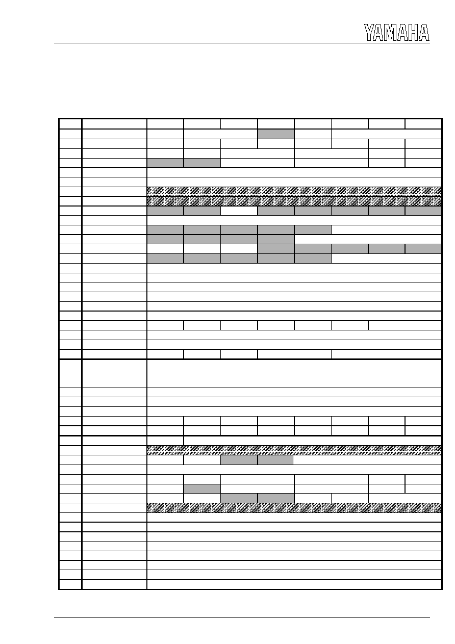
2. Control Register / Register Map
The decoding system is controlled by reading and writing the control registers as shown below through
microprocessor interfaces (/CS, SCK, SI, SO).
All bits are set to "0" by initial clear (/IC= "L").
Address
Name
bit 7
bit 6
bit 5
bit 4
bit 3
bit 2
bit 1
bit 0
0x00
AUTO/DSN
AUTOMOD
PD1-0
DSNIGN
DSN2-0
0x01
MUTE
LMUTEN
CMUTEN
RMUTEN
RSMUEN
LSMUTEN
LFEMUTEN DSPMUTEN
AMOFF
0x02
SDIA
SDIACKSEL
SDIASEL
SDIAFMT1-0
SDIABIT1-0
SDIAWP
SDIABP
0x03
SDOA
SDOAFMT1-0
SDOABIT1-0
SDOAWP
SDOABP
0x04
OPORT
OPORT7-0
0x05
IPORT
IPORT7-0
0x06
(TEST)
0x07
(TEST)
0x08
PCM
PCMDLY
0x09
NOISE LEVEL
NOISELEV7-0
0x0A
CENTER DELAY
CDELAY2-0
0x0B
SURROUND DELAY
SRDELAY3-0
0x0C
NOISE
NOISE
PN/WN
IMPULSE
0x0D
FS
FS2-0
0x0E
L VOLUME
LVOL7-0
0x0F
C VOLUME
CVOL7-0
0x10
R VOLUME
RVOL7-0
0x11
LS VOLUME
LSVOL7-0
0x12
RS VOLUME
RSVOL7-0
0x13
LFE VOLUME
LFEVOL7-0
0x14
COMPRESSION
EMPON
AIBON
VOLON
DITHOFF
P11OFF
DIALOFF
COMPMOD1-0
0x15
HDYNRNG
HDYNRNG7-0
0x16
LDYNRNG
LDYNRNG7-0
0x17
MODE
PCMMOD PLDECON PLSRMOD
DUALMOD1-0
OUTMOD2-0
0x18
|
0x2A
BITSTREAM
(described in the later section)
0x2B
(Unused)
(Undefined)
0x2C
(Unused)
(Undefined)
0x2D
Pc
Pc7-0
0x2E
DATA STREAM
STREAM7 STREAM6 STREAM5 STREAM4 STREAM3 STREAM2 STREAM1 STREAM0
0x2F
STATUS
DTSDATA AC3DATA 2/0MODE
SURENC
KARAOKE
MUTE
CRC
NONPCM
0x30
ZERO
ZEROFLG
ZERO6-0
0x31
(TEST)
0x32
MPCNT_H
MPLOAD
MPCLEAR
N
MPCNT11-8
0x33
MPCNT_L
MPCNT7-0
0x34
SDIB
SDIBCKSEL
SDIBSEL
SDIBFMT1-0
SDIBBIT1-0
SDIBWP
SDIBBP
0x35
SDOB
SDOBCKSEL
SDOBFMT1-0
SDOBBIT1-0
SDOBWP
SDOBBP
0x36
ERAM
OVFSEL
JMPSEL
RASREF ERAMMOD
ERAMSEL1-0
0x37
(TEST)
0x38
MI0
MI0REG7-0
0x39
MI1
MI1REG7-0
0x3A
MI2
MI2REG7-0
0x3B
MI3
MI3REG7-0
0x3C
MI4
MI4REG7-0
0x3D
MI5
MI5REG7-0
0x3E
MI6
MI6REG7-0
0x3F
MI7
MI7REG7-0

YSS922
14
0x40
DIR CTRL
CKMOD
VUCMUTE SDOMUTE
DDINSEL1-0
0x41
DIR SDO
LOCKMOD1-0
DIROFMT1-0
DIROBIT1-0
DIROWP
DIROBP
0x42
DIR PIN
BSMOD
VMOD
UMOD
CMOD
CTIMMOD
0x43
DIR INTMOD
INTMOD6-0
0x44
(TEST)
0x45
DIR CUADR
DHLD
R/L
U/C
CUADR4-0
0x46
DIR CUDAT
CUDAT7-0
0x47
DIR STATUS
DIRINT
DIRERR
LOCKN
VFLAG
CSB1
CSCHG
BSFLAG
SLIP
0x48
DIR FS
CSB3
DIRFS2-0
0x49
DIR FSCNT
FSCNT7-0
0x4A
|
0x57
(TEST)
0x58
|
0x7F
Invalid
The output at the SO pin becomes High-Z.
Never write "1" into the shaded bits because the bits for testing are assigned there.
Never make an access to addresses 0x06, 0x07, 0x31, 0x37, 0x44, 0x4A to 0x57 because the registers for
testing are assigned there.

YSS922
15
∑ The contents of the bitstream register (addresses 0x18 to 0x2A) vary depending on the input signal, i.e., the Main
DSP input signal is AC-3 bitstream, DTS bitstream or PCM as shown below.
Only reading is allowed to the BITSTREAM register and not writing.
∑ When the input signal is AC-3 bitstream
Address
Name
bit 7
bit 6
bit 5
bit 4
bit 3
bit 2
bit 1
bit 0
0x18
BITSTREAM 0
fscod
frmsizecod
0x19
BITSTREAM 1
bsid
bsmod
0x1A
BITSTREAM 2
acmod
cmixlev
surmixlev
lfeon
0x1B
BITSTREAM 3
dsurmod
copyrightb
origbs
0
0
0
0
0x1C
BITSTREAM 4
0
0
0
dialnorm
0x1D
BITSTREAM 5
0
0
0
dialnorm2
0x1E
BITSTREAM 6
audprodie
mixlevel
roomtyp
0x1F
BITSTREAM 7
audprodi2e
mixlevel2
roomtyp2
0x20
BITSTREAM 8
timecod1e
0
timecod1
0x21
BITSTREAM 9
timecod1
0x22
BITSTREAM 10
timecod2e
0
timecod2
0x23
BITSTREAM 11
timecod2
0x24
BITSTREAM 12
langcode
langcod2e
compre
compr2e
0
0
0
0
0x25
BITSTREAM 13
langcod
0x26
BITSTREAM 14
langcod2
0x27
BITSTREAM 15
compr
0x28
BITSTREAM 16
compr2
0x29
BITSTREAM 17
dynrng
0x2A
BITSTREAM 18
dynrng2
∑ When the input signal is DTS bitstream
Address
Name
bit 7
Bit 6
bit 5
bit 4
bit 3
bit 2
bit 1
bit 0
0x18
BITSTREAM 0
fscod
(Undefined)
RATE
0x19
BITSTREAM 1
(Undefined)
0x1A
BITSTREAM 2
AMODE
(Undefined)
lfeon
0x1B
BITSTREAM 3
(Undefined)
PCMR
0x1C
|
0x23
BITSTREAM 4
|
BITSTREAM 11
(Undefined)
0x24
BITSTREAM 12
(Undefined)
DYNF
(Undefined)
0x25
BITSTREAM 13
(Undefined)
0x26
BITSTREAM 14
(Undefined)
0x27
BITSTREAM 15
RANGE
0x28
BITSTREAM 16
(Undefined)
0x29
BITSTREAM 17
(Undefined)
0x2A
BITSTREAM 18
(Undefined)
∑ When the input signal is PCM
The contents of BITSTREAM register (addresses 0x18 to 0x2A) are all undefined.

YSS922
16
3. Serial Data Interface
Shown below are interface formats obtained by setting to SDIA register, SDOA register, SDIB register, SDOB
register and DIR SDO register.
M
L
L
L
L
W P = 0
W P = 1
B P = 0
B P = 1
F M T 1 - 0 = 0 0
B I T 1 - 0 = X X
F M T 1 - 0 = 1 0
B I T 1 - 0 = X X
F M T 1 - 0 = 0 1
B I T 1 - 0 = 0 0
F M T 1 - 0 = 0 1
B I T 1 - 0 = 0 1
F M T 1 - 0 = 0 1
B I T 1 - 0 = 1 0
F M T 1 - 0 = 0 1
B I T 1 - 0 = 1 1
W C K
B C K
D A T A
L c h ( L s , C c h )
R c h ( R S , L F E c h )
1 F r a m e
M
L
M
L
M
L
M
L
8 7
M
L
6 5
M
L
4 3
M
L
M
8 7
M
6 5
M
4 3
M
L
M : MSB L : LSB
L
N o D e l a y
I2S
E I A J

YSS922
17
4. Microprocessor Interface Format
A four-wire serial interface is used to read and write the control registers.
A 1
A 0
A 2
A 3
A 4
A 5
A 6
D 0
D 1
D 2
D 3
D 4
D 5
D 6
D 7
D o n ' t C a r e
D o n ' t C a r e
A 1
A 0
A 2
A 3
A 4
A 5
A 6
D o n ' t C a r e
D o n ' t C a r e
D o n ' t C a r e
R / W
R / W
D 0
D 1
D 2
D 3
D 4
D 5
D 6
D 7
H i g h - Z
H i g h - Z
H i g h - Z
/ C S
S C K
SI
S O
S O
SI
write
R / W = L
r e a d
R / W = H
SO becomes an output pin only when all of the following conditions are met.
∑ /CS= "L"
∑ When reading the valid addresses
∑ Timing of 8 bits data output
If any of the above conditions is not met, SO outputs High-Z. Thus, SO, SI and SCK can be used jointly with
other devices that have similar interfaces.
The microprocessor interface functions even when the power down mode.

YSS922
18
ELECTRICAL CHARACTERISTICS
1. Absolute Maximum Ratings
Parameter
Symbol
Condition
Min.
Typ.
Max.
Unit
Power Supply Voltage
V
DD1
AV
DD
V
DD2
Vss-0.5
Vss-0.5
Vss-0.5
Vss+4.6
Vss+4.6
Vss+3.6
V
V
V
Input Voltage
VI
-0.5
Vss+5.75
V
Storage Temperature
Tstg
-50
125
∞C
2. Recommended Operating Conditions
Parameter
Symbol
Condition
Min.
Typ.
Max.
Unit
Power Supply Voltage
V
DD
1
AV
DD
V
DD
2
3.0
3.0
2.3
3.3
3.3
2.5
3.6
3.6
2.7
V
V
V
Operating Temperature
Top
0
25
70
∞C
3. DC Characteristics (Under recommended operating conditions)
Parameter
Symbol
Condition
Min.
Typ.
Max.
Unit
Input voltage "H" level 1
V
IH1
*1
0.7V
DD1
V
Input voltage "L" level 1
V
IL1
*1
0.3V
DD1
V
Input voltage "H" level 2
V
IH2
*2
2.2
V
Input voltage "L" level 2
V
IL2
*2
0.8
V
Output voltage "H" level
V
OH
I
OH
= -80µA
2.4
V
Output voltage "L" level
V
OL
I
OL
= 1.0mA
0.4
V
Input leakage current
I
LI
no pull-up
-10
10
µA
Pull-up resistor
R
U
40
160
k
W
Power Consumption
P
D1
V
DD1
TBD
TBD
mW
P
D2
V
DD2
TBD
TBD
mW
*1: Applicable to XI pin.
*2: Applicable to input pins except XI.

YSS922
19
SYSTEM CONNECTION DIAGRAM
Y S S 9 2 2
( A C 3 D 3 )
A D C
D A C
S D I A
D A I F
( S P D I F )
D D I N 0
XI
H O S T
P R O C E S S O R
/CS
SCK
SI
SO
XO
D A C
D A C
D A C
( o p t i o n )
A N A L O G
L
R
DIRMCK
DIRBCK
DIRWCK
(256fs)
(64fs)
(fs)
(256fs)
(64fs)
(fs)
S D O B 0
S D O B 1
S D O B 2
S D O B 3
L
R
L S
R S
C
L F E
S R A M o r D R A M
( o p t i o n )
D D I N 1
D D I N 2
D D I N 3
2 4 . 5 7 6 M H z
CPO
D I R P C O
4 7 0 0 p F
1 0 k o h m
4 7 0 p F
RAMD0-15 CASN RASN RAMWEN RAMOEN RAMA0-17
/IC
/IC
TESTXI
D I R P R O
A V S S
5 . 1 k o h m

YSS922
20
EXTERNAL DIMENSIONS
YSS922
21
MEMO
YSS922
22
IMPORTANT NOTICE
1. Yamaha reserves the right to make changes to its Products and to this document without
notice. The information contained in this document has been carefully checked and is believed
to be reliable. However, Yamaha assumes no responsibilities for inaccuracies and makes no
commitment to update or to keep current the information contained in this document.
2. These Yamaha Products are designed only for commercial and normal industrial
applications, and are not suitable for other uses, such as medical life support equipment,
nuclear facilities, critical care equipment or any other application the failure of which could lead
to death, personal injury or environmental or property damage. Use of the Products in any such
application is at the customer's sole risk and expense.
3. YAMAHA ASSUMES NO LIABILITY FOR INCIDENTAL, CONSEQUENTIAL OR SPECIAL
DAMAGES OR INJURY THAT MAY RESULT FROM MISAPPLICATION OR IMPROPER USE
OR OPERATION OF THE PRODUCTS.
4. YAMAHA MAKES NO WARRANTY OR REPRESENTATION THAT THE PRODUCTS ARE
SUBJECT TO INTELLECTUAL PROPERTY LICENSE FROM YAMAHA OR ANYTHIRD
PARTY, AND YAMAHA MAKES NO WARRANTY OR REPRESENTATION OF NON-
INFRINGEMENT WITH RESPECT TO THE PRODUCTS. YAMAHA SPECIFICALLY
EXCLUDES ANY LIABILITY TO THE CUSTOMER OR ANY THIRD PARTY ARISING FROM
OR RELATED TO THE PRODUCTS' INFRINGEMENT OF ANY THIRD PARTY'S
INTELLECTUAL PROPERTY RIGHTS, INCLUDING THE PATENT, COPYRIGHT,
TRADEMARK OR TRADE SECRET RIGHTS OF ANY THIRD PARTY.
5. EXAMPLES OF USE DESCRIBED HEREIN ARE MERELY TO INDICATE THE
CHARACTERISTICS AND PERFORMANCE OF YAMAHA PRODUCTS. YAMAHA ASSUMES
NO RESPONSIBILITY FOR ANY INTELLECTUAL PROPERTY CLAIMS OR OTHER
PROBLEMS THAT MAY RESULT FROM APPLICATIONS BASED ON THE EXAMPLES
DESCRIBED HEREIN. YAMAHA MAKES NO WARRANTY WITH RESPECT TO THE
PRODUCTS, EXPRESS OR IMPLIED, INCLUDING, BUT NOT LIMITED TO THE
WARRANTIES OF MERCHANTABILITY, FITNESS FOR A PARTICULAR USE AND TITLE.
Note) The specifications of this product are subject to improvement change without prior notice.
AGENCY
YAMAHA CORPORATION
Address inquires to :
Semi-conductor Sales & Marketing Department
- Head Office
203, MatsunokiJima, Toyooka-mura.
Iwata-gun, Shizuoka-ken, 438-0192
Tel. +81-539-62-4918 Fax. +81-539-62-5054
- Tokyo Office
2-17-11, Takanawa, Minato-ku, Tokyo, 108-8568
Tel. +81-3-5488-5431 Fax. +81-3-5488-5088
- Osaka Office
1-13-17, Namba Naka, Naniwa-ku,
Osaka City, Osaka, 556-0011
Tel. +81-6-6633-3690 Fax. +81-6-6633-3691
- U.S.A. Office
YAMAHA System Technology.
100 Century Center Court, San Jose, CA 95112
Tel. +1-408-467-2300 Fax. +1-408-437-8791
COPYING PROHIBITED © 2000 YAMAHA CORPORATION