FP64
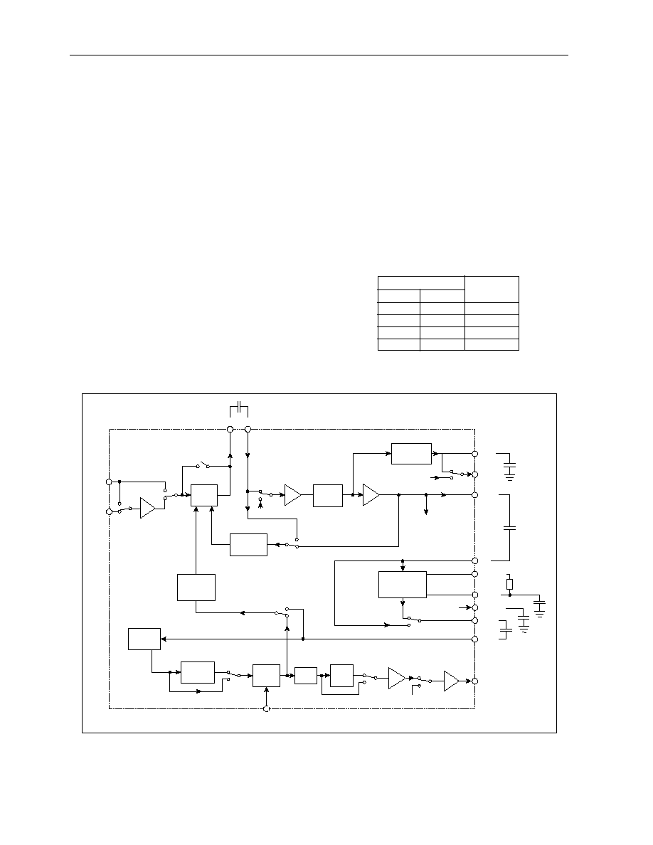
ACE9040 provides all the speech signal processing and
data/SAT tone filtering needed for AMPS or TACS analog
cellular telephones.
Transmit voice channel functions comprise a microphone
amplifier, soft limiter, bandpass filter, compressor, hard
limiter, lowpass filter and a gain controlled amplifier to set
deviation level. Additional transmit circuits include a DTMF
generator, data and SAT filters, deviation setting amplifiers for
data/ST and SAT and a modulation combiner.
ACE9040's receive path comprises a bandpass filter,
expander, volume control and power amplifiers to directly
drive an earpiece or handsfree transducer.
Gain settings, mute switches and filter characteristics are
programmed via a three wire serial interface.
To implement a handsfree function, both transmit and
receive paths have rectifiers for signal amplitude monitoring
via an external pin and signal path attenuators controlled via
the serial interface.
ACE9040 combines minimum power consumption with
low external component count. Standby modes greatly reduce
supply current and extend battery charge intervals.
Features
∑
Low Power and Low Voltage (3∑6 to 5∑0 V) Operation
∑
Power Down Modes
∑
Direct Connections to Microphone and Earpiece
∑
Compander with wide operating range:
Compressor 74 db typ., Expander 36 dB typ.
∑
SAT Bandpass and Data Lowpass Filters
∑
Handsfree Operation Supported
∑
DTMF Generator
∑
Serial Bus Controlled Gains and Filter Responses
∑
Part of the ACE Integrated Cellular Phone Chipset
∑
TQFP 64 Pin 10X10 mm or 7X7 mm Packages
Applications
∑
AMPS and TACS Cellular Telephones
∑
Two-Way Radio Systems
Related Products
ACE9040 is part of the following chipset:
∑
ACE9020 Receiver and Transmitter Interface
∑
ACE9030 Radio Interface and Twin Synthesiser
∑
ACE9050 System Controller and Data Modem
Absolute Maximum Ratings
Supply voltage 6 V
Storage temperature - 55
∞C to + 150 ∞C
Operating temperature - 40
∞C to + 85 ∞C
Voltage at any pin - 0.3 V to V
DD
+ 0.3 V
ACE9040
Audio Processor
Advance Information
DS4289
ISSUE 4.1
January 2001
Ordering Information
Industrial temperature range
ACE9040J/IW/FP1N
64 lead (10x10mm) LQFP
T
rays
. Bake
and dry pack
.
ACE9040J/IW/FP1Q
64 lead (10x10mm) LQFP
Tape and Reel. Bake and dry pack
ACE9040J/IW/FP2N
64 lead (7x7mm) LQFP
T
rays
. Bake
and dry pack
.
ACE9040J/IW/FP2Q
64 lead (7x7mm) LQFP
Tape and reel. Bake
and dry pack
.
AMP
MI
MODULATION
SUMMING
AMPLIFIER
DTMF
DATI
TSI
RSI
COMPRESSOR
DATA FILTER
(LOW PASS)
GENERATE/
TRANSPOND
FILTERS AND
DEVIATION SET
DTMF
GEN.
TX SAT
FILTER
RX SAT
FILTER
RX
FILTER
SET
LEVELS
CONTROL
LOGIC
EXPANDER
RXI
SCLK
LEN
SD
STBY
SET DEVIATION
VOLUME
LINE OUTPUT
LO
EPON
EPOP
RSO
TSO
DATO
MOD
SUMO
SUMI
TLPO
FEED-
BACK
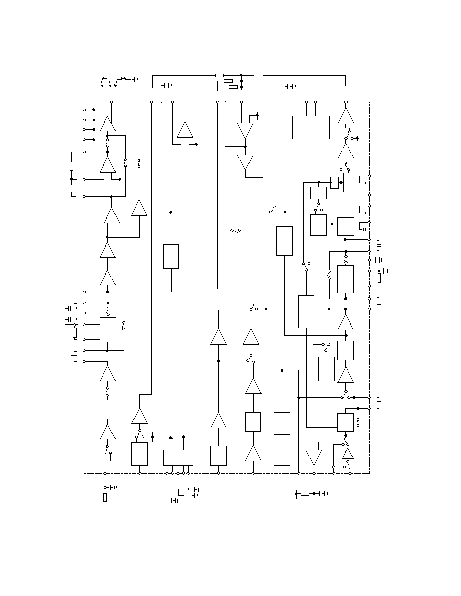
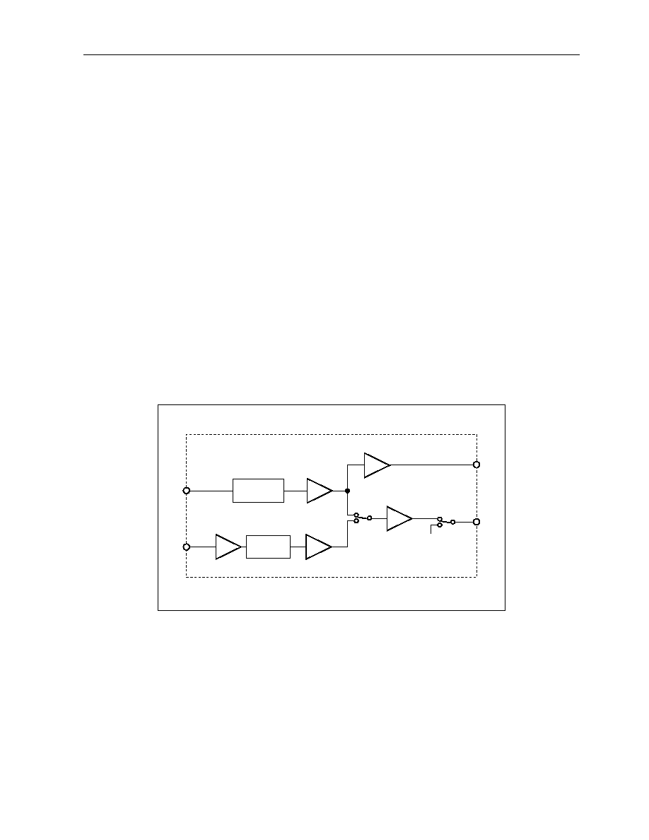
Figure 2 - ACE9040 Simplified Block Diagram
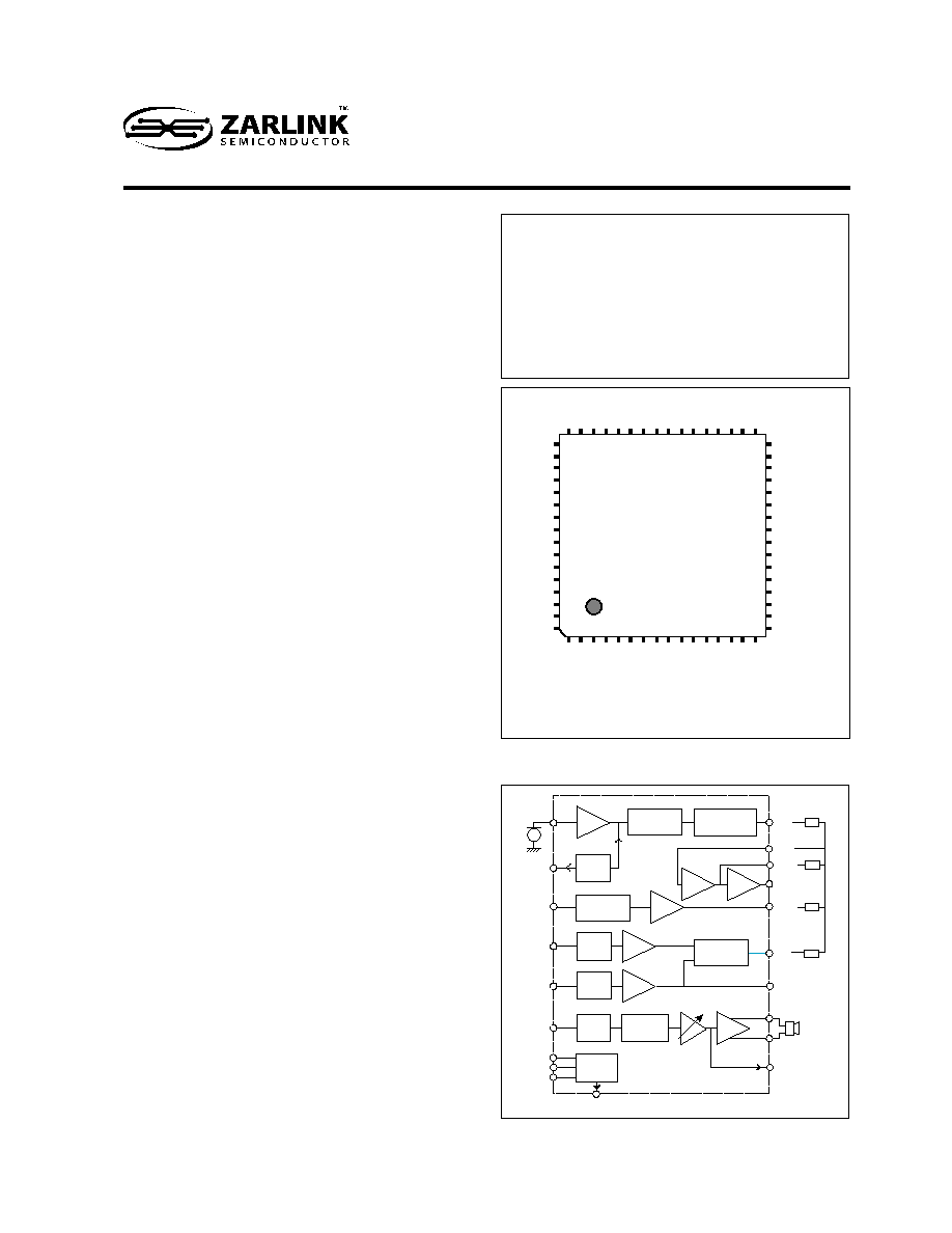
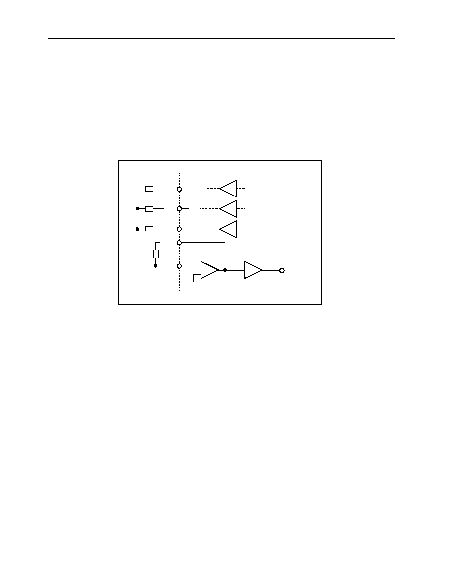
Figure 1 - Pin connections - top view
Note: Pin 1 is identified by moulded spot and
by coding orientation. (* 7 x 7 mm package and
10 x10 mm package pinouts on page 3)
FP64
nc
nc\DVSS*
AMPI
nc\LEN*
PREIN
DVSS\DVDD*
TBPO
LEN\VMIDRX*
CIN
DVDD\LO*
CRCIN
VMIDRX\STBY*
VMIDTX
LO\EVDD*
CRCOUT
STBY\EPON*
nc
EVDD\nc*
COUT
EPON\nc*
TXC
EVSS
RXC
EPOP
IPS
EAMPFB
SLO
EAMPO
MI
EIN
MICBIAS
ERCOUT
VDD
AMPO
DEC
DTMF
HF
nc
LI
V485
RREF
BGAP
BIAS
TLPO
A
VDD
SUMI
DA
TI
SUMO
TSI
MOD
RSI
A
VSS
RXI
DA
T
O
RBPO
TSO
EAMPI
RSO
HFGIN
SD
EOUT
SCLK
ERCIN
L
V
N
ACE9040
1
2
ACE9040
Advance Information
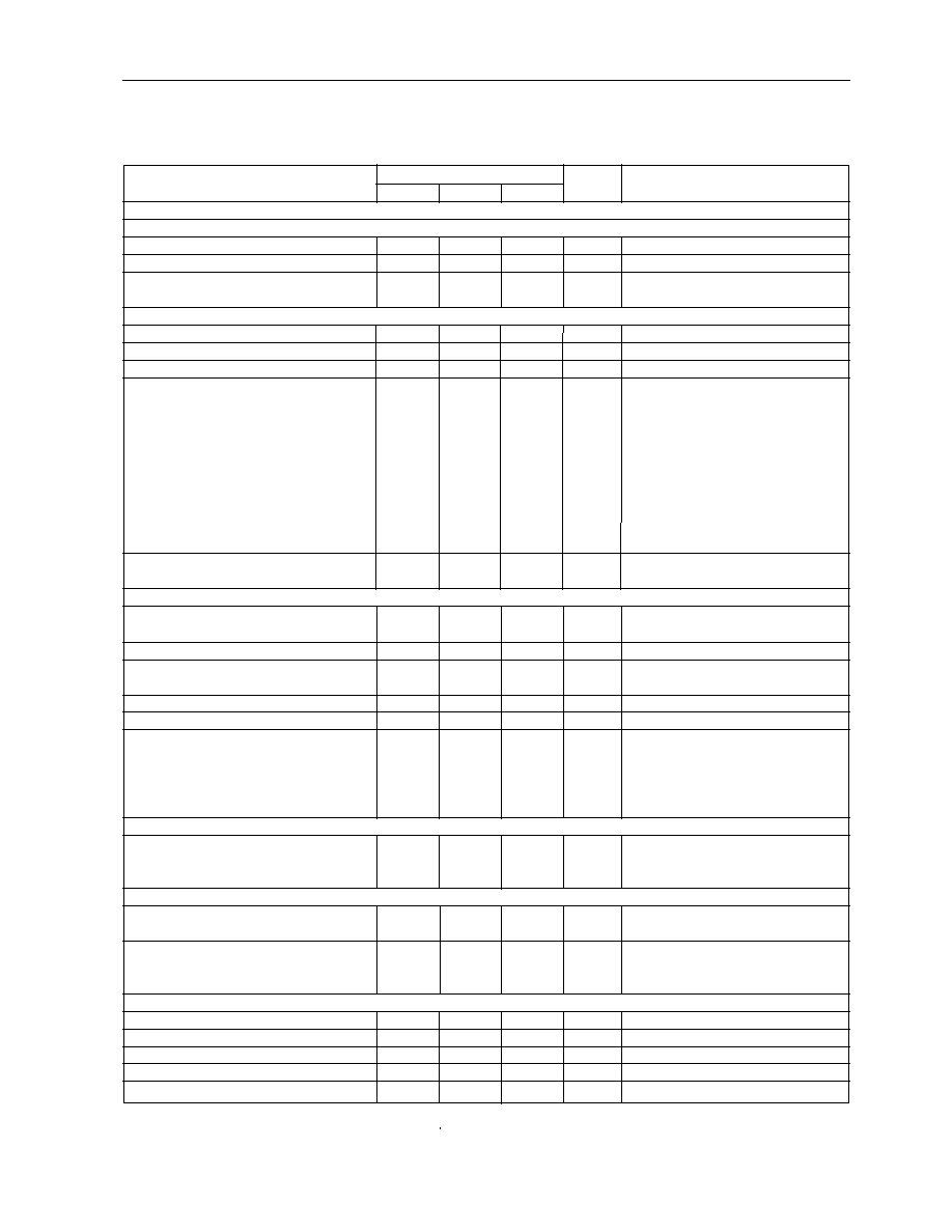
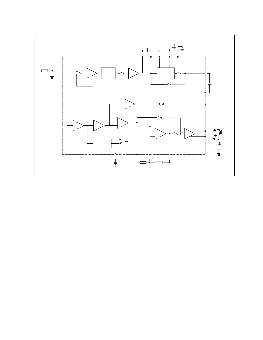
Figure 3 - ACE9040 Detailed Block Diagram
180K
10nF
3.3
µ
F
RXI
DA
TI
8
LOW P
ASS
FIL
TER
11
T
ONEM
VMIDRX
DA
TM
VMIDRX
VMIDTX
BIAS
GENERAT
OR
2
6
5
64
44
DEC
BIAS
RREF
MICBIAS
BGAP
100/
68*k
10nF
*VDD = 3.75V
RSI
10
RXSA
T
FIL
TER
9
TSI
-12 dB / 0 dB
DTMF
47
DTMF
VDO
220 k
33
LV
N
_
+
Vth
VDD
4
63
LI
MLI
MI
SLO
IPS
10nF
SOFT
LIMITER
62
61
INPSENSE
DTMFM
92% DETECT
LEVEL
DTMF
MODE
PRE-
EMPHASIS
TXSA
T
FIL
TER
-15dB
SA
TS
10dB
DA
T
ADEV
RXBPF
RXM
EXPGAIN
12
18
16
17
27
15
VMIDRX
33nF
RBPO
EIN
ERCOUT
ERCIN
EOUT
HFGIN
EXP
ANDER
100nF
82nF
10nF
COMP[2:1]
SCHMITT
SA
TDEV
VMIDRX
3 & 97%
DETECT
LEVELS
TEST
[1:0]
TXBPF
HFGAIN
10nF
180k
100nF
COMPRESSOR
52
53
56
54
55
58
51
TBPO
CIN
CRCOUT
CRCIN
COUT
PREIN
A
VSS
DVSS
V485
EVSS
33nF
82nF
39
30
45
22
GAIN
CONTROL
TEST
[2:1]
TEST
[1:0]
PRE-
EMPHASIS
HANDSFREE
RECTIFIER
RXC
HFS
TXC
SD
HANDSFREE
RECTIFIER
RXLEVEL
HF
A
TTEN
SIDET
ONE
LODRIVE
EARSENSE
14
EAMPI
EAMPFB
EAMPO
13
20
19
EAMP
_
+
VMIDRX
SUB
12
4
7
2
8
VDD
EVDD
A
VDD
DVDD
21
23
EPH0/
EPH1
EPH0/EPH1
26
HIZ
38
EPOP
EPON
LO
DA
T
O
60
50
48
_
+
VMIDTX
TXSENSE
_
+
VMIDTX
36
37
41
42
40
3
59
HARD
LIMIT
-8 dB
TEST[0]
TXLPF
TXM
VMIDTX
AUDIODEV
TLPO
DRIVER
43
TLPO
SERIAL
INTERF
ACE
25
29
35
34
STBY
LEN
SD
SCLK
TXC 68nF
SUMI
MOD
HF
TSO
SUMO
RSO
RXC
AMPI
AMPO
68nF
33
µ
F
64
150
MIS

Advance Information
3
ACE9040
Pin No.
Pin No.
Name
Description
FP2 package FP1 package
1
1
V
DD
V
DD
supply to substrate, pin should be at highest d.c. voltage
2
2
DEC
Mid-supply reference decoupling connection, 3.3
µF to GND
3
3
HF
Output from TX or RX handsfree rectifier, switched by bit "HFS"
4
4
LI
Line input
5
5
RREF
Reference bias current set for all op-amps by resistor to GND
6
6
BIAS
Buffered mid-supply reference output
7
7
AV
DD
Analogue V
DD
input
8
8
DATI
Transmit data input
9
9
TSI
SAT path input for locally generated tone
10
10
RSI
SAT path receiver input for received tone
11
11
RXI
Speech path receiver input
12
12
RBPO
Audio output from EXPGAIN block
13
13
EAMPI
Output from EARSENSE amp
14
14
HFGIN
Input to RX volume control and handsfree attenuator
15
15
EOUT
Expander speech output
16
16
ERCIN
Expander time constant input, 180 k
to ERCOUT, 100 nF to GND
17
17
ERCOUT
Expander time constant output, 180 k
to ERCIN
18
18
EIN
Expander speech input, 33 nF to RBPO
19
19
EAMPO
Output from EAMP op-amp
20
20
EAMPFB
Inverting input to EAMP op-amp
21
21
EPOP
Earpiece driver positive output
22
22
EV
SS
Earpiece V
SS
(GND) supply connection
-
23/24
nc
No connection
23
25
EPON
Earpiece driver negative output
24
26
EV
DD
Earpiece V
DD
supply input
25
27
STBY
Standby output: low indicates standby state, high is V
DD
output @ 10 mA
26
28
LO
Line output
27
29
VMIDRX
RX path mid-supply reference voltage, 82 nF to GND
28
30
DV
DD
Digital V
DD
29
31
LEN
Serial interface latch signal input, rising edge triggered
30
32
DV
SS
Digital V
SS
(GND) connection
31/32
-
nc
No connection
33
33
LVN
Low supply V
DD
voltage indicator comparator output, reset active low output
34
34
SCLK
Serial interface system clock input
35
35
SD
Serial interface data input
36
36
RSO
Received (regenerated) SAT output
37
37
TSO
Transmit SAT output, regenerated or transponded
38
38
DATO
Transmit data filter output.
39
39
AV
SS
Analogue V
SS
(GND)
40
40
MOD
Modulation output: sum of Speech, Data and SAT
41
41
SUMO
Modulation summing amplifier output
42
42
SUMI
Modulation summing amplifier input
43
43
TLPO
Transmit audio lowpass filter output
44
44
BGAP
Bandgap voltage output, 10 nF to GND
45
45
V485
Hard limiter gain selection for 3.75 V or 4.85 V nominal supplies
46
46
nc
No connection
47
47
DTMF
DTMF tone output
48
48
AMPO
Auxillary op-amp output
49
49
nc
No connection
50
50
AMPI
Auxillary op-amp inverting input (non-inverting internally connected to VMIDTX)
51
51
PREIN
Transmit pre-emphasis filter input
52
52
TBPO
Transmit bandpass filter output
53
53
CIN
Compressor audio input, 10 nF from TBPO
54
54
CRCIN
Compressor time constant input, 100 nF to GND, 180 k
to CRCOUT
55
55
VMIDTX
TX path reference voltage, 82 nF to GND
56
56
CRCOUT
Compressor time constant output, 180 k
to CRCIN
57
57
nc
No connection
58
58
COUT
Compressor audio output, 33 nF to PREIN
59
59
TXC
Transmit handsfree audio level sensing rectifier smoothing filter, 68 nF to GND
60
60
RXC
Received handsfree audio level sensing rectifier smoothing filter, 68 nF to GND
61
61
IPS
Transmit audio gain INPSENSE adjustment block input
62
62
SLO
Soft limiter output
63
63
MI
Microphone input
64
64
MICBIAS
Bias for electret or active microphone
PIN Descriptions
Note: FP1 = 10 x 10mm package, FP2 = 7 x 7 mm package

4
ACE9040
Advance Information
Characteristic
Symbol
Value
Unit
Conditions
Min.
Typ.
Max.
Supply Current and Power Down Modes
Operating supply current
I
DD
15
mA
V
DD
= 4.85 V R
REF
= 100 k
15
mA
V
DD
= 3.75 V R
REF
= 68 k
Standby
Attenuation of all inputs signals
40
dB
Wakeup response time
10
ms
Sleep (Standby with CLK stopped)
Supply current*
I
DD(SLEEP)
200
µA
STBY bit set V
DD
= 3.75
Delay between setting STBY bit and
20
µs
stopping clock
Delay to starting clock after wakeup
100
µs
Characteristic
Value
Unit
Conditions
Min.
Typ.
Max.
Transmission Path
Microphone Amp, MI to SLO pins
Input bias
V
DD
/2
Internal 150 k
bias resistor to V
DD
/2
Microphone input gain (LO)
21
22
23
dB
MIS = 1, MLI = 0, MIG = 0
Microphone input gain (HI)
31
32
33
dB
MIS = 1, MLI = 0, MIG = 1
Microphone crosstalk (no MI signal)
≠ 40
dB
MIS = 1, MLI = 0, MIG = 1
Line input, LI to SLO pins
Input bias
V
DD
/2
Internal 100 k
bias resistor
LI input Gain (0dB)
≠ 0.5
0.5
dB
MIS = 0, MLI = 0, MIG = 0
LI input Gain (LO)
21
22
23
dB
MIS = 1, MLI = 1, MIG = 0
LI input gain (HI)
31
32
33
dB
MIS = 1, MLI = 1, MIG = 1
LI input crosstalk (no LI signal)
≠ 40
dB
MIS = 1, MLI = 1, MIG = 1
Soft Deviation Limiter, LI to SLO pins
Nominal gain
0
dB
Limiter not functioning.
Attenuation range
≠ 30
≠ 29
dB
Attenuation steps
0.27
0.5
0.67
dB
Distortion
2
%THD
Output at 1 Vrms
Attack level:Hard limiter output
3
97
% V
DD
Attack level at TBPO pin
92
% V
DD
d.c. input at IPS
TEST[1:0] = 11
Attack time
40
µs
Per gain step when signal outside
threshold
Decay time
1.68
ms
Per gain step
INPSENSE Gain Stage, IPS to TBPO pins
Nominal gain
7.5
8
8.5
dB
Input = 100 mV
rms,
INPS[4:0] = 15, THF = 0 dB,
Gain adjustment range
≠ 12
12.8
dB
Relative to nominal gain
Input = 100 mV
rms,
Gain step size
0.6
0.8
1.2
dB
INPS[4:0] = 0 to 31, THF = 0 dB
Electrical Characteristics
These characteristics are guaranteed over the following conditions unless otherwise stated (Note 1):
T
AMB
= ≠ 40
∞C to + 85 ∞C, V
DD
= 3.6 V to 5.0 V
Note 1. 100% production tested at 25
∞C but guaranteed over specified temperature range.
* Standby current measured with the 1.008 MHz clock stopped and SCLK at a level <200 mV.

Advance Information
5
ACE9040
Characteristic
Value
Unit
Conditions
Min.
Typ.
Max.
TX Audio Bandpass Filter TXBPF, IPS to TBPO
Noise
≠ 72
dBV
Distortion
1
%THD
1 Vrms output
Frequency response relative to 1040 Hz
≠ 60.5
≠ 38.5
dB
f = 60 Hz
≠ 25.5
≠ 10.5
dB
f = 184 Hz INPSENSE = 0 dB
≠ 1.0
+ 0.5
dB
f = 430 Hz THF = 0 dB
≠ 0.5
+ 0.5
dB
f = 676 Hz, 1040 Hz
≠ 0.5
+ 0.5
dB
f = 1410 Hz, 1900 Hz
≠ 1.5
≠ 0.5
dB
f = 3260 Hz
≠ 3.0
≠ 1.5
dB
f = 3500 Hz
≠ 10.5
≠ 5
dB
f
= 4120 Hz
≠ 20.5
≠ 15.5
dB
f = 5590 Hz
≠ 90.5
≠ 30.5
dB
f = 9900 Hz
TX Handsfree Gain Stage HFGAIN
Nominal gain
0
dB
Gain range
≠ 52.5
≠ 49
≠ 45.5
dB
THF[2:0] = 0 to 7
Gain step size
6.5
7
7.5
dB
0 to ≠21 dB
Gain step size
5
7
9
dB
≠28 to ≠49 dB
TX Compressor Stage, CIN to COUT pins
Unity gain level
636
707
777
mVrms
= Vref (Unaffected level)
Input range
0.79
1000
mVrms
Linearity CIN to COUT:
± 0.5
dB
CIN = Vref + 3 dB to Vref - 59 dB
(Deviation from 2:1 I/O relationship)
BW = 300 Hz to 3.4 kHz
Attack time
3
ms
12 dB step: - 8 dB to - 20 dB relative
to the unity gain (Vref) level
Decay time
13.5
ms
Attack & Decay levels = 1.5 and 0.75
of steady state final value
Distortion
2
%THD
BW = 300 Hz - 3.4 kHz
Frequency response
± 0.2
dB
BW = 300 Hz - 3.4 kHz
TX Pre-emphasis, PREIN to TLPO pins
Input impedance
75
k
Internal compressor and BAR:
Nominal gain TACS
≠ 7.5
≠ 7
≠ 6.5
dB
COMP[2:1] = 10 or 01 at 1 kHz
Nominal gain AMPS
≠ 11.5
≠ 11
≠ 10.5
dB
External compressor and bypass:
Nominal gain AMPS & TACS
≠ 0.5
0
+ 0.5
dB
COMP[2:1] = 11 or 00 at 1 kHz
Frequency response
5.8
6
6.2
dB/
TEST[1:0] = 01
Octave
PREEMPH = 0 (active)
f = 300 to 3400 Hz
Electrical Characteristics
These characteristics are guaranteed over the following conditions unless otherwise stated (Note 1):
T
AMB
= ≠ 40
∞C to + 85 ∞C, V
DD
= 3.6 V to 5.0 V

6
ACE9040
Advance Information
Characteristic
Value
Unit
Conditions
Min.
Typ.
Max.
Hard Deviation Limiter
Gain
13
13.5
14
dB
V485 pin = 0 V (for V
DD
= 3.75 V)
15.5
16
16.5
dB
V485 pin = V
DD
(for V
DD
= 4.85 V)
Low Pass Filter TXLPF, PREIN to TLPO pins
Distortion
1.5
%THD
1.5 Vp-p Output level
Noise
≠ 60
dBV
BW = 30 Hz to 30 kHz
Frequency response TACS/AMPS
0.3
0.7
dB
f = 307 Hz
Relative to 1 kHz
≠ 0.5
+ 0.5
dB
f = 676 Hz, 1040 Hz
≠ 0.5
+ 0.5
dB
f = 1410 Hz, 1900 Hz
≠ 3.0
≠ 1.5
dB
f = 3010 Hz
≠ 38.0
≠ 13.0
dB
f = 3500 Hz
≠ 60.0
≠ 38.0
dB
f = 4120 Hz
≠ 60.0
≠ 38.0
dB
f = 5590 Hz
≠ 60.0
≠ 38.0
dB
f = 9900 Hz
≠ 60.0
≠ 35.0
dB
f = 11870 Hz
≠ 60.0
≠ 35.0
dB
f = 14950 Hz
Gain
≠ 8.5
≠ 8
≠ 7.5
dB
Attenuation with TXLPF bypassed
8
dB
TEST[0] = 1
Gain Stage AUDIODEV, PREIN to TLPO
Nominal gain
0
dB
Output at TLPO
Gain adjustment
- 2.8
3.2
dB
Attenuation step size
0.2
0.4
0.6
dB
Control bits: AUDEV[3:0]
TXM switch attenuation
≠ 60
dB
AUDIODEV = 0 dB
Combined TX path
Gain with 3.5
µV at Microphone input
33.5
37.5
dB
INSENSE = 0 dB, V485 = 0 V
Distortion
1.0
% THD
THF & AUDIODEV = 0 dB
Noise
≠ 55.0
dBV
MI gain = 22 dB, V
DD
= 3.6 V
Output d.c. level
1.65
1.9
V
Compressor Bypassed
Electrical Characteristics
These characteristics are guaranteed over the following conditions unless otherwise stated (Note 1):
T
AMB
= ≠ 40
∞C to + 85 ∞C, V
DD
= 3.6 V to 5.0 V
Advance Information
7
ACE9040
Electrical Characteristics
These characteristics are guaranteed over the following conditions unless otherwise stated (Note 1):
T
AMB
= ≠ 40
∞C to + 85 ∞C, V
DD
= 3.6 V to 5.0 V
Characteristic
Value
Unit
Conditions
Min.
Typ.
Max.
Receive Path
RX Input stage RXSENSE, RXI to RBPO pins
Input bias
V
DD
/2
Internally biased to V
DD
/2 by 150 k
Nominal gain
7.25
8
8.75
dB
Gain adjustment range
≠ 6
6.4
dB
Input 40 mVrms at RXI
Gain adjustment step size
0.2
0.4
0.6
dB
RXM = 1, RXSENSE = 0 to 31
RX Audio Bandpass Filter RXBPF
Gain
0
dB
Distortion
1
%THD
At 1 kHz with 40 mVrms input
Noise
≠ 65
dB
BW= 30 Hz to 30 kHz
Frequency Response
≠ 90.0
≠ 45.0
dB
f = 60 Hz RXSENSE = 0 dB
Relative to 1040 Hz
≠ 15.0
≠ 7.0
dB
f = 184 Hz
COMP[1:0] = 00
≠ 2.0
+ 0.5
dB
f = 430 Hz
≠ 0.5
+ 0.5
dB
f = 676 Hz, 1040 Hz
≠ 0.5
+ 0.5
dB
f = 1410 Hz, 1900 Hz
≠ 3.0
≠ 0.5
dB
f = 3260 Hz
≠ 10.0
≠ 6.0
dB
f = 3500 Hz
≠ 40.0
≠ 25.0
dB
f = 4120 Hz
≠ 40.0
≠ 25.0
dB
f = 5590 Hz
≠ 90.0
≠ 40.0
dB
f = 9900 Hz
RXM mute switch attenuation
≠ 40
dB
Output switched to V
DD
/2 when
muted.
Rx Internal Expander
Gain EXPGAIN: internal
11.8
12.3
12.8
dB
COMP[2:1] = 10
external and bypass
0
dB
COMP[2:1] = 00 or 11
Unity gain level
850
1000
1200
mVrms
= Vref (Unaffected level)
Linearity EIN to EOUT
± 1
dB
EIN = Vref to Vref - 33 dB
(Deviation from 2:1 input/output)
BW = 300 to 3400 Hz
Distortion
2
%THD
1 Vrms
Frequency response
± 0.2
dB
300 to 3400 Hz
Attack time
3
ms
6 dB step (- 4 dB and -10 dB) relative
to the unity gain (Vref) level at 1 kHz
to pin EIN. Output at EOUT.
Decay time
13.5
ms
Attack and delay time levels = 0.57
and 1.5 of final steady state value.
RX Volume Control RXLEVEL
Nominal Gain
≠ 11
≠ 12
≠ 13
dB
RXV[2:0] = 3, RHF = 0 dB
Gain adjustment range
≠ 9
12
dB
RXV[2:0] = 0 to 7
Gain adjust step size
2
3
4
dB
EARSENSE = 0 dB, Sidetone = 0 dB
RX Handsfree Gain Stage HFATTEN
HFGAIN to EAMP nominal gain
≠ 0.4
0
0.4
dB
RHF, RVX, EARSENSE = 0 dB,
SD =0
Gain range
≠ 52.5
≠ 49
≠ 45.5
dB
RHF[2:0] = 0 to 7
Gain control step size
6.5
7
7.5
dB
0 to ≠ 21 dB
Gain control step size
5
7
9
dB
≠ 28 to ≠ 49 dB
RX Line Driver LODRIVE
LO gain
4
5
6
dB
RVX = 0 dB, RHF = 0 dB, HIZ =1
Distortion
2
%THD
1.0 Vrms output
LO mute
≠ 40
dB
HIZ = 0
Noise
≠ 80
dBV
BW = 30 Hz to 30 kHz
LOoutput during mute
1.5
V
DD
/2
2.1
V
V
DD
= 3.6 V

8
ACE9040
Advance Information
Characteristic
Value
Unit
Conditions
Min.
Typ.
Max.
Rx Earpiece Gain Adjustment EARSENSE
Nominal gain
0
dB
Total gain
- 2.8
3.2
dB
EARS[3:0] = 0 to 15
Gain adjustment step size
0.2
0.4
0.6
dB
RVX = 0 dB, RHF = 0 dB, SD = 0
Distortion
1
% THD
Output 1 Vrms
Rx Sidetone Path, IPS to EAMPI
Attenuation at EARSENSE amp input
18
19
20
dB
EARSENSE = 0 dB
Sidetone mute
≠ 40
dB
SD = 0
Rx Earpiece Drivers EPOP & EPON
EPON single ended gain
5.5
6
6.5
dB
Output = 2 Vpp,
120
EPON to EPOP
EPOP single ended d.c. level
1.7
V
DD
/2
1.9
V
V
DD
= 3.6 V, EPH1 = 1, EPH0 = 0
EPOP single ended a.c. level
≠ 20
dB
EPON single ended distortion
1
% THD
Output = 2 Vpp
EPON & EPOP differential gain
11.5
12
12.5
dB
150
(± 20 %) EPON to EPOP
EPOP differential distortion
1
%THD
Output = 4 Vpp, EPH1 = 1, EPH0 = 1
Earpiece mute switch attenuation
40
dB
EPH0 = 0 & EHP1 = 0
EPON external mode:
64
(± 20 %) + 3.3 µF to GND,
EPON gain relative to EAMPI
5.5
6.5
dB
EAMPFB open, Input = HFGIN
EPON distortion
1
% THD
Output = 1.1 Vpp
EPOP output current external mode
≠ 10
10
µA
At V
DD
& 0 V
EPON & EPOP mute
≠ 40
dB
EPH1 = 0, EPH0 = 0
EPOP Noise
≠ 80
dBV
EPH1 = 1, EPH0 = 1
Transmit Data Path
TX Data Filter 16 kHz & 20 kHz
Input bias at DATI
V
DD
/2
V
Internally tied via 800 k
resistor to
V
DD
/2.
Nominal gain
- 6.5
- 6
- 5.5
dB
Input = 1 Vrms
Distortion
1.5
%THD
Output = 1.5 Vp-p
Noise
-60
dBV
BW = 30 Hz to 30 kHz
DATM mute switch attenuation
40
dB
Data Filter frequency response
16 kHz (TACS)
≠ 0.3
0.3
dB
f = 676 Hz, 1040 Hz
≠ 0.3
0.3
dB
f = 4120 Hz
≠ 0.1
≠ 0.7
dB
f = 12120 Hz
≠ 0.9
≠ 1.6
dB
f = 13960 Hz
≠ 2.5
≠ 1.5
dB
f = 14950 Hz
DATM = 1
≠ 5.0
≠ 2.0
dB
f = 16050 Hz
DATADEV = 0 dB
≠ 5.0
≠ 3.0
dB
f = 16420 Hz
Relative to 1040 Hz
≠ 6.0
≠ 4.0
dB
f = 17040 Hz
DATAF[1:0] = 10
≠ 7.0
≠ 5.0
dB
f = 18020 Hz
≠ 11.0
≠ 9.0
dB
f = 19990 Hz
≠ 12.0
≠ 10.0
dB
f = 20970 Hz
Electrical Characteristics
These characteristics are guaranteed over the following conditions unless otherwise stated (Note 1):
T
AMB
= ≠ 40
∞C to + 85 ∞C, V
DD
= 3.6 V to 5.0 V

Advance Information
9
ACE9040
Characteristic
Value
Unit
Conditions
Min.
Typ.
Max.
TX Data Filter 16 kHz & 20 kHz (continued)
Data Filter frequency response
20 kHz (AMPS)
≠ 0.3
0.3
dB
f = 676 Hz, 1040 Hz
≠ 0.3
0.3
dB
f = 4120 Hz, 16050 Hz
≠ 0.3
≠ 1.5
dB
f = 16050 Hz
≠ 2.5
≠ 1.0
dB
f = 18020 Hz
≠ 3.0
≠ 1.5
dB
f = 18880 Hz DATAF[1:0] = 11
≠ 4.0
≠ 2.0
dB
f = 20240 Hz DATM = 1
≠ 5.0
≠ 3.0
dB
f = 20540 Hz DATADEV = 0dB
≠ 5.5
≠ 3.5
dB
f = 20970 Hz Relative to 1040 Hz
≠ 7.0
≠ 5.0
dB
f = 21960 Hz
≠ 8.0
≠ 6.0
dB
f = 22820 Hz
≠ 10.0
≠ 8.0
dB
f = 24050 Hz
TX Data Gain Stage DATADEV, DATI to DATO pins
Nominal gain
0
dB
Gain adjustment
- 2.8
3.2
dB
DATD[3:0] = 7
Gain adjustment steps
0.2
0.4
0.6
dB
DATM = 1 DATAF[1:0] = 00
TXSAT and RXSAT Bandpass Filters 6 kHz
RXSAT Filter
RXSAT gain
9
11
dB
Input = 400 mVrms at 6030 Hz,
SATDEV = 0 dB, SATM = 1,
SATS = 0dB
RXSAT 6 kHz frequency response
≠ 90.0
≠ 35.0
dB
f = 2520 Hz Relative to 6030 Hz
≠ 90.0
≠ 35.0
dB
f = 3500 Hz
SATS = 0 dB,
≠ 90.0
≠ 35.0
dB
f = 4120 Hz
TACS = 1,
≠ 29.0
≠ 24.0
dB
f = 4980 Hz
SATD = 15 (0 dB),
≠ 0.30
0.50
dB
f = 5900 Hz
SATM = 1
≠ 0.10
0.35
dB
f = 5960 Hz
≠ 0.10
0.35
dB
f = 6030 Hz
≠ 0.30
0.6
dB
f = 6090 Hz
≠ 26.5
≠ 22.0
dB
f = 7010 Hz
≠ 90.0
≠ 29.0
dB
f = 8060 Hz
≠ 90.0
≠ 35.0
dB
f = 9040 Hz
≠ 90.0
≠ 35.0
dB
f = 9290 Hz
RSO Schmitt output
5.5
6.0
6.5
kHz
SATS = 0 dB, TACS = 1
Electrical Characteristics
These characteristics are guaranteed over the following conditions unless otherwise stated (Note 1):
T
AMB
= ≠ 40
∞C to + 85 ∞C, V
DD
= 3.6 V to 5.0 V

10
ACE9040
Advance Information
Characteristic
Value
Unit
Conditions
Min.
Typ.
Max.
TXSAT Filter 6 kHz
TXSAT gain
≠ 29.0
≠ 25.0
dB
TACS =1, SATS = 1, Output = 1 Vpp
at 6030 Hz
TXSAT 6 kHz frequency response
≠ 90.0
≠ 35.0
dB
f = 2520 Hz Relative to 6030 Hz
≠ 90.0
≠ 35.0
dB
f = 3500 Hz
SATS = 1
≠ 90.0
≠ 35.0
dB
f = 4120 Hz
TACS = 1
≠ 29.0
≠ 24.0
dB
f = 4980 Hz
SATD = 15 (0 dB)
≠ 0.30
0.50
dB
f = 5900 Hz
SATM = 1
≠ 0.10
0.35
dB
f = 5960 Hz
≠ 0.10
0.35
dB
f = 6030 Hz
≠ 0.30
0.50
dB
f = 6090 Hz
≠ 26.5
≠ 22.0
dB
f = 7010 Hz
≠ 60.0
≠ 35.0
dB
f = 8060 Hz
≠ 60.0
≠ 35.0
dB
f = 9040 Hz
≠ 80.0
≠ 35.0
dB
f = 9290 Hz
TXSAT Noise
≠ 71.0
dBV
Gain Stage SATDEV
Nominal gain
0
dB
Gain adjustment range
- 4.5
4.8
dB
SATS = 0, TACS = 1, SATM = 1
Gain adjustment size
0.05
0.3
0.55
dB
SATD[4:0] = 0 to 31
Distortion
2
% THD
Output = 1.1 Vpp
SATM switch mute attenuation
40
dB
SATM = 0
DTMF Generator
DTMF output level
60
85
mVrms
V
DD
= 3.6 V, high & low tone
DTMF single tone distortion:
TONEM switch on (via TBPO)
5
% THD
Low group, TONEM = 1
TONEM switch off
≠ 40
dB
TONEM = 0
DTMF switch on (via RBPO)
5
% THD
High group, DTMFM = 1
DTMF switch off
≠ 40
dB
DTMFM = 0
DTMF high group pre-emphasis
≠ 0.5
0.5
dB
DTWIST = 0
1.5
2.5
dB
DTWIST = 1
Gain Stage TXSENSE, SUMI to MOD pins
Gain
- 0.5
0
0.5
dB
Output at MOD.
Gain adjustment
- 2.8
3.2
dB
TXSEN[3:0] = 0 to 15
Gain adjustment step size
0.2
0.4
0.6
dB
Distortion
2
%THD
Output = 1 Vrms
Noise
≠ 80
dBV
BW = 30 Hz to 30 kHz
Electrical Characteristics
These characteristics are guaranteed over the following conditions unless otherwise stated (Note 1):
T
AMB
= ≠ 40
∞C to + 85 ∞C, V
DD
= 3.6 V to 5.0 V

Advance Information
11
ACE9040
Electrical Characteristics
These characteristics are guaranteed over the following conditions unless otherwise stated (Note 1):
T
AMB
= ≠ 40
∞C to + 85 ∞C, V
DD
= 3.6 V to 5.0 V
Characteristic
Value
Unit
Conditions
Min.
Typ.
Max.
Handsfree Rectifiers
Attack time
1
ms
Capacitors to GND =
Decay time
35
ms
68 nF at TXC & RXC pins
TX nominal output levels:
V
DD
= 3.75 V
d.c. offset
0.3
0.5
V
Input at IPS = 0 mVrms
a.c. level
1.4
1.5
1.65
V
Input at IPS = 40 mVrms, 1 kHz
INPSENSE = 0 dB, HFS = 0
HFP = 1
RX nominal output levels:
V
DD
= 3.75 V
d.c. offset
0.3
0.5
V
Input at HFGIN = 0 mVrms
a.c. level
1
1.1
1.2
V
Input at HFGIN = 100 mVrms, 1 kHz
HFS =1, HFP = 1
Voltage Outputs
DEC & BIAS output voltage
1.70
(V
DD
-V
SS
)/2
1.9
V
V
DD
= 3.6 V, 3.3
µF decoupling to
GND at DEC pin
Microphone Bias: Source 1 mA
2.7
2.9
V
MLI = 0, MIS = 1, V
DD
= 3.6 V
Sink 1 mA
2.7
2.9
V
MLI = 0, MIS = 1, PD = 0
Microphone disabled
≠ 0.1
0.10
V
MLI = 0, MIS = 0
External Reference Resistor
100
k
V
DD
= 4.85 V
connected from pin RREF to GND
68
k
V
DD
= 3.75 V
Bandgap at BGAP
1.10
1.35
V
LVN Supply Voltage Comparator
Default condition
V
DD
= 3.6 V
≠ 10
10
µA
(high at V
DD
≠ 0.2 V)
V
DD
= 3.1 V
2.00
20.0
mA
(low at 0.4 V)
LVN comparator operating lower limit
1
V
of V
DD
12
ACE9040
Advance Information
Figure 3a - Serial Interface Input Timing
Electrical Characteristics
These characteristics are guaranteed over the following conditions unless otherwise stated (Note 1):
T
AMB
= ≠ 40
∞C to + 85 ∞C, V
DD
= 3.6 V to 5.0 V
Characteristic
Symbol
Value
Unit
Conditions
Min.
Typ.
Max.
DC Characteristics
Logic input high
V
IH
0.7 x V
DD
V
DD
+ 0.3
V
Logic input low
V
IL
- 0.3
0.3 x V
DD
V
Input Capacitance
C
in
10
pF
logic inputs leakage current
I
ILK
± 1
µA
SCLK, SD, LEN inputs
V
DD
= 3.6 V & 0.0 V
AC Characteristics
Clock input frequency: Serial
f
CLK
1.008
MHz
interface & SC Filters
-100
100
ppm
Deviation from 1.008 MHz
Clock duty cycle
D
40
50
60
%
Number of clock rising edges to
24
clock
input data
cycles
Clock cycles between latch pulses
30
clock
on LEN
cycles
Clock cycles before power-up and
8
clock
after powerdown
cycles
Data setup time
t
ds
80
ns
V
DD
= 3.75 V
± 0.1 V.
Data hold time
t
dh
80
ns
T
A
= - 40
∞C to + 85 ∞C
Clock low
t
cll
400
600
ns
Clock high
t
clh
400
600
ns
Clock high to latch high
t
cl
440
ns
Latch high to clock high
t
lc
220
ns
Latch high
t
lh
240
ns
Rise and fall times
50
ns
All digital inputs
Power Supply Rejection Ratio:
PSRR
V
DD
= 3.8 V + 100 mVpp (a.c.)
COMP[2:1] = 00.
TX path (LI to TLPO)
≠ 12
dB
LI = 0 dB, V485 = 13.5 dB
INPSENSE = 0 dB, softlimit on.
RX path (RXI to EPOP)
≠ 20
dB
AUDIODEV, RXSENSE = 0 dB
THF, RHF, EARSENSE = 0 dB
RXV, SIDETONE off.
Crosstalk TX to RX
-45
dB
MOD = 0.2 V
RMS
(MOD to EPOP/EPON)
t
lh
t
cl
t
lc
t
clh
t
cll
t
ds
t
dh
SCLK
Data
Latch
Advance Information
13
ACE9040
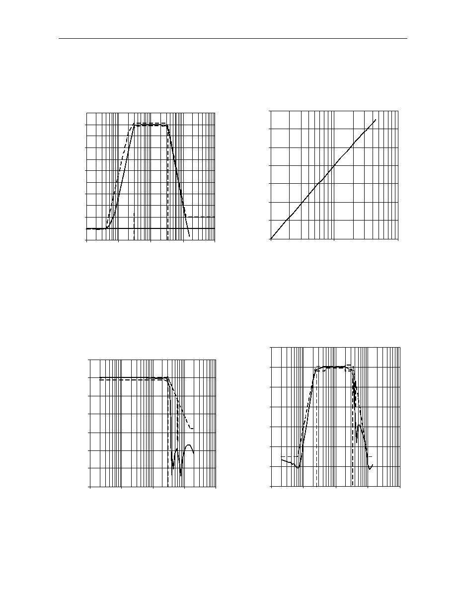
Typical Frequency Responses
Figure 5
Figure 6
Figure 7
Figure 4
TXBPF Relative Response
vs
Frequency
Frequency (Hz)
Re
l
a
t
i
v
e
Re
s
p
o
n
s
e
(d
B
)
-50
-40
-30
-20
-10
0
10
100
1000
10000
100000
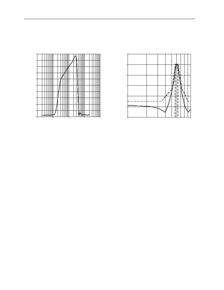
Pre-emphasis Relative Response
vs
Frequency
Frequency (Hz)
R
e
l
a
t
i
v
e
R
esp
o
n
se
(d
B
)
-20
-15
-10
-5
0
5
10
15
100
1000
10000
TXLPF Relative Response
vs
Frequency
Frequency (Hz)
R
e
l
a
t
i
v
e
R
esp
o
n
se
(d
B
)
-60
-50
-40
-30
-20
-10
0
10
10
100
1000
10000
100000
RXBPF Relative Response
vs
Frequency
Frequency (Hz)
R
e
l
a
t
i
v
e
R
esp
o
n
se
(d
B
)
-60
-50
-40
-30
-20
-10
0
10
10
100
1000
10000
100000
14
ACE9040
Advance Information
Figure 9
Figure 8
Typical Frequency Responses
Transmit Overall Relative
Response vs Frequency
Frequency (Hz)
R
e
l
a
t
i
v
e
R
esp
o
n
se
(d
B
)
-40
-35
-30
-25
-20
-15
-10
-5
0
5
10
10
100
1000
10000
100000
SAT Filter Relative Response
vs
Frequency
Frequency (Hz)
R
e
l
a
t
i
v
e
R
esp
o
n
se
(d
B
)
-50
-40
-30
-20
-10
0
10
1000
10000
Advance Information
15
ACE9040
Description
the control bits for one of the standards are set, others are
under user control.
Power saving operates when an individual block is de-
selected and for the whole circuit when in Standby. The circuit
combines high performance with minimum power
consumption and uses as few external components as
possible.
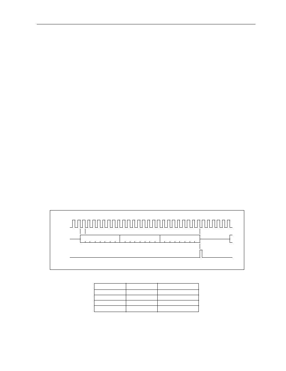
Serial Control Bus
All functions are controlled via a three wire serial
interface. Input is via pins SD for serial data, SCLK for the clock
input and LEN for the control message latch signal.
Incoming data bits are clocked in on the rising edges of
SCLK clock input. At the end of each control message
comprising three 8-bit data bytes, the rising edge of the LEN
pulse latches in the data. A system controller should clock
data out on clock falling edges to ensure the maximum timing
margins.
The SCLK clock input must be at 1∑008 MHz and
continuous whenever the ACE9040 is active because
ACE9040's switched capacitor filters use clocks derived from
SCLK to set frequency responses.
ACE9040 expects a minimum of 30 clock cycles between
LEN latch pulses, including the clock cycle containing the latch
pulse. A minimum of 8 clock cycles before the beginning of an
Operate command or after a Standby command are expected.
Three data bytes DATA1, DATA2, and DATA3 contain
bits for system selection, control and mute switches, gain
control and filter response settings, as shown in figure 10. The
last two bits of DATA3, DATA3[1] and [0], determine the
message type, either "Operation", "Initializing mode 0",
"Initializing mode 1" or "Handsfree". The details of these four
modes are described in tables 2 to 19.
ACE9040 combines all the voice, data and signalling
processing circuits for analog cellular telephones operating
with the AMPS or TACS systems.
Transmit channel functions comprise a microphone
amplifier, soft limiter, bandpass speech filter, compressor,
pre-emphasis filter, hard limiter, lowpass transmit filter and a
gain control stage to set the deviation. Additional transmit
circuits include a DTMF generator, a lowpass filter for either
control data or signalling tone (ST), filters for supervisory
audio tone (SAT), either transponded or locally re-generated,
and deviation setting amplifiers for Data, ST and SAT. The
outputs from the transmit functions feed a modulation
combiner whose gain can be adjusted before driving a
modulator and external power amplifier.
ACE9040's receive path consists of a bandpass filter,
expander, volume control and power amplifier to directly drive
the earpiece, either differentially or in single ended modes.
Sidetone and DTMF tones can be introduced into the receive
path.
Gain settings, filter characteristics and system control is
programmed via a three wire serial interface to give optimum
operation with either the AMPS or TACS analog cellular
systems.
To implement a handsfree function, both transmit and
receive paths have rectifiers which enable signal amplitude
monitoring via an external pin and signal path attenuators
controlled via the serial interface.
All filter characteristics are set by ratioed on-chip
components and by a fixed externally input clock rate of
1∑008 MHz and do not need trimming, filter response options
are selected via the serial interface.
Gain adjustments for different system specifications and
component tolerancing are set via the serial interface using
gain control blocks in the transmit and receive signal paths.
These eliminate the need for any mechanically adjusted
potentiometers. Some gain levels change automatically when
DATA3[1]
DATA3[0]
Mode
0
1
"Operation"
0
0
"Initializing mode 0"
1
0
"Initializing mode 1"
1
1
"Handsfree"
Figure 10 - Serial Receive Bus Timing
Table 1 - Mode Selections
DATA1
DATA2
DATA3
SCLK
SD
LEN
7 6 5 4 3 2 1 0 7 6 5 4 3 2 1 0 7 6 5 4 3 2 1 0
EARLIEST
START OF
NEXT
MESSAGE

16
ACE9040
Advance Information
EPH1
EPH0
Function
0
0
Earphone mute
0
1
External Earpiece (EPON to ground)
1
0
Single ended output (EPON to EPOP)
1
1
Differential output (EPON and EPOP)
MLI
MIS
Function
0
0
LI selected, no gain
0
1
MI selected, Micamp gain
1
0
NOT ALLOWED
1
1
LI selected, Micamp gain
Data bit
Bit Name
Function
Effect when
Effect when
at 0
at 1
DATA3:
[0]
DATA3[0]
Bus Mode Select
Must be "1"
Must be "1"
[1]
DATA3[1]
Bus Mode Select
Must be "0"
Must be "0"
[2]
PD
Power Down
Operate
Standby
[5:3]
RXV[2:0]
Receive Volume
See table 3
See table 3
[6]
HIZ
Line Output Drive Enable
Off
On
[7]
EPH1
Earpiece Mute
See table 5
See table 5
DATA2:
[0]
RXM
Receiver Audio Mute
Muted
On
[1]
SATM
Transmit SAT Mute
Muted
On
[2]
DATM
Transmit Data Mute
Muted
On
[3]
TXM
Transmit Audio Mute
Muted
On
[4]
MLI
Microphone Select
See table 4
See table 4
[5]
DTMFEN
Enables each DTMF tone selection
Disabled
Enabled
[7:6]
DTMFMODE[1:0]
DTMF Tone Select
See table 6
See table 6
DATA1:
[0]
DTMFM
Transmit DTMF Switch
Speech
DTMF
[1]
TONEM
DTMF RX path Confirm Tone Switch
Speech
DTMF
[5:2]
DTMF[3:0]
DTMF Code Select
See table 7
See table 7
[6]
MIS
Line Input Select
See table 4
See table 4
[7]
PREEMPH
Transmit Pre-emphasis Bypass
Active
Bypassed
RXV[2]
RXV[1]
RXV[0]
Gain in dB
0
0
0
≠ 21
0
0
1
≠ 18
0
1
0
≠ 15
0
1
1
≠ 12
1
0
0
≠ 9
1
0
1
≠ 6
1
1
0
≠ 3
1
1
1
0
Table 3 - Receiver Volume Control Nominal Levels set by
RXV[2:0].
Table 4 - Microphone Input Select
Table 5 - Earphone Mode Select
(EHP0 in Initializing mode 0)
DTMFMODE[1:0] bits
Tone generated
1 and 0
0 and 0
No tone.
0 and 1
Low frequency only.
1 and 0
High frequency only.
1 and 1
Dual tones.
Table 6 - DTMF Mode Selection
Control Bus: Operation Mode
DTMF[3:0] bits Keypad
Low Freq.
High Freq.
3 2 1 0
legend
Hz.
Hz.
0 0 0 0
1
697
1209
0 0 0 1
2
697
1336
0 0 1 0
3
697
1477
0 0 1 1
A
697
1633
0 1 0 0
4
770
1209
0 1 0 1
5
770
1336
0 1 1 0
6
770
1477
0 1 1 1
B
770
1633
1 0 0 0
7
852
1209
1 0 0 1
8
852
1336
1 0 1 0
9
852
1477
1 0 1 1
C
852
1633
1 1 0 0
*
941
1209
1 1 0 1
0
941
1336
1 1 1 0
#
941
1477
1 1 1 1
D
941
1633
Table 2 - "Operation Mode", DATA3[1:0] = 01.
Table 7 - DTMF Tones

Advance Information
17
ACE9040
Data bit
Bit Name
Function
Effect when
Effect when
at 0
at 1
DATA3:
[0]
DATA3[0]
Bus Mode Select
Must be "0"
Must be "0"
[1]
DATA3[1]
Bus Mode Select
Must be "0"
Must be "0"
[2]
EPH0
Earpiece Mode Select
See table 5
See table 5
[3]
DTWIST
DTMF Pre-emphasis
0 dB
2 dB
[4]
PDLVC
Power Supply Comparator
Active
Power Down
[6:5]
COMP[2:1]
Compander Control
See table 9
See table 9
[7]
INPS[0]
Transmit Audio Gain Adjust
See table 10
See table 10
DATA2:
[3:0]
INPS[4:1]
Transmit Audio Gain Adjust
See table 10
See table 10
[7:4]
RXSEN[3:0]
Receive Audio Gain Adjust
See table 11
See table 11
DATA1:
[0]
RXSEN[4]
Receive Audio Gain Adjust
See table 11
See table 11
[5:1]
SATD[4:0]
SAT Modulation Gain
See table 12
See table 12
[6]
SD
Sidetone Enable
Off
On
[7]
SOFTLIMIT
Enables Softlimiter
Off
On
Table 8 - "Initializing Mode 0", DATA3[1:0] = 00.
INPS[4] INPS[3] INPS[2] INPS[1] INPS[0]
Gain (dB)
0
0
0
0
0
≠ 12∑0
0
0
0
0
1
≠ 11∑2
:
:
:
:
:
:
:
:
:
:
:
:
1
1
1
1
0
+ 12∑0
1
1
1
1
1
+ 12∑8
COMP[2]
COMP[1]
Mode
0
0
Bypass Compander
1
0
Internal Compander
1
1
External Compander
0
1
BAR Signal Input Mode
(RBPO at high impedance)
RXSEN[4]
RXSEN[3]
RXSEN[2]
RXSEN[1]
RXSEN[0]
Gain (dB)
0
0
0
0
0
≠ 6∑0
0
0
0
0
1
≠ 5∑6
:
:
:
:
:
:
:
:
:
:
:
:
1
1
1
1
0
+ 6∑0
1
1
1
1
1
+ 6∑4
SATD[4]
SATD[3]
SATD[2]
SATD[1]
SATD[0]
Gain (dB)
0
0
0
0
0
≠ 4∑5
0
0
0
0
1
≠ 4∑2
:
:
:
:
:
:
:
:
:
:
:
:
1
1
1
1
0
+ 4∑5
1
1
1
1
1
+ 4∑8
Table 9 - Compander Operating Modes set by COMP[2:1].
Table 10 - INPSENSE Transmit Audio Nominal Gain
settings by INPS[4:0].
Table 11 - RXSENSE Receive Audio Nominal Gain settings by RXSEN[4:0].
Table 12 - SATDEV Transmit SAT Nominal Modulation Gain settings by SATD[4:0].
Control Bus: Initializing Mode 0

18
ACE9040
Advance Information
TXSEN[3]
TXSEN[2]
TXSEN[1]
TXSEN[0]
DATD[3]
DATD[2]
DATD[1]
DATD[0]
Gain
AUDEV[3]
AUDEV[2]
AUDEV[1]
AUDEV[0]
(dB)
EARS[3]
EARS[2]
EARS[1]
EARS[0]
0
0
0
0
≠ 2∑8
0
0
0
1
≠ 2∑4
:
:
:
:
:
:
:
:
:
:
1
1
1
0
+ 2∑8
1
1
1
1
+ 3∑2
Data bit
Bit Name
Function
Effect when
Effect when
at 0
at 1
DATA3:
[0]
DATA3[0]
Bus Mode Select
Must be "0"
Must be "0"
[1]
DATA3[1]
Bus Mode Select
Must be "1"
Must be "1"
[3:2]
TEST[1:0]
Test Mode Select
see table 14
see table 14
[4]
SATS
SAT source Select
RXSAT
TXSAT
[6:5]
DATAF[1:0]
Data Filter Bandwidth Select
see table 15
see table 15
[7]
TACS
Cellular System Select
TACS
DATA2:
[3:0]
TXSEN[3:0]
Combined Modulation Gain
see table 16
see table 16
[7:4]
DATD[3:0]
Data Modulation Gain
see table 16
see table 16
DATA1:
[3:0]
AUDEV[3:0]
Audio Modulation Gain
see table 16
see table 16
[7:4]
EARS[3:0]
Earpiece "EARSENSE" Gain
see table 16
see table 16
Control Bus: Initializing Mode 1
TEST[1]
TEST[0]
Test Mode
0
0
Operate mode (not in test mode)
1
0
Test DTMF
0
1
Bypass TXLPF
1
1
Bypass TXLPF & Softlimiter test
Table 14 - Test Modes selected by TEST[1:0].
Table 15 - Data Filter Bandwidths selected by DATAF[1:0].
Table 16 - TXSENSE, DATADEV, AUDIODEV, and EARSENSE
Nominal Gains set, respectively, by TXSEN[3:0], DATD[3:0],
AUDEV[3:0], and EARS[3:0].
DATAF[1]
DATAF[0]
Cut-off Frequency
1
0
16 kHz
1
1
20 kHz
See table 19.
Table 13 - "Initializing Mode 1", DATA3[1:0] = 10.

Advance Information
19
ACE9040
Control Bus: Handsfree Mode
Data bit
Bit Name
Function
Effect when
Effect when
at 0
at 1
DATA3:
[0]
DATA3[0]
Bus Mode Select
Must be "1"
Must be "1"
[1]
DATA3[1]
Bus Mode Select
Must be "1"
Must be "1"
[4:2]
THF[2:0]
Transmit Handsfree Gain
see table 18
see table 18
[7:5]
RHF[2:0]
Receive Handsfree Gain
see table 18
see table 18
DATA2:
[0]
HFP
Handsfree Rectifiers Power
Off
On
[1]
HFS
HF Output Connection Path
Transmit
Receive
[2]
MIG
Microphone Amplifier Gain
+ 22 dB
+ 32 dB
[4:3]
not used
-
-
-
[5]
AMPS
Cellular System Select
AMPS
[6]
not used
-
-
-
[7]
-
-
must be "0"
must be "0"
DATA1:
[2:0]
-
-
must be "0"
must be "0"
[5:3]
not used
-
-
-
[7:6]
not used
-
-
-
THF[2]
THF[1]
THF[0]
Gain
RHF[2]
RHF[1]
RHF[0]
(dB)
0
0
0
0
0
0
1
≠ 7
0
1
0
≠ 14
0
1
1
≠ 21
1
0
0
≠ 28
1
0
1
≠ 35
1
1
0
≠ 42
1
1
1
≠ 49
Table 18 - TXHFGAIN and RXHFGAIN Handsfree
Attenuator Nominal Gains, set by THF[2:0] and RHF[2:0].
See table 19.
Table 17 - "Handsfree Mode", DATA3[1:0] = 11.
20
ACE9040
Advance Information
Circuit Operating Modes
ACE9040 has three operating modes: Operate, Standby
and Sleep. In Operate mode all parts of the circuit are active,
except for any explicitly powered down and the DTMF genera-
tor which only powers up when tones are generated. The pin
STBY is pulled high in Operate mode to supply V
DD
to external
audio circuits, such as a compander.
Standby Mode
Standby mode is used when the cellular terminal is
waiting for a call and is selected by an "Operation mode"
control message with bit PD at "1". In this mode all analog
circuits, data paths, filters and their clock drivers are powered
down giving a greatly reduced supply current. In standby
mode all switch and level controls retain their previous state,
the pin STBY is not driven removing the V
DD
supply from
external circuits. To leave Standby mode an operate com-
mand should be given by using an "Operation mode" control
message with bit PD at "0".
Sleep Mode
Sleep mode is the same as Standby but without a clock
input. To enter sleep mode the standby command should be
given and after a delay of at least 20
µs the SCLK clock
stopped. To wake-up from sleep mode, the the SCLK clock
must be started and after a delay of at least 100
µs an operate
command given.
Power on Reset
At power up ACE9040 is put into Standby mode.
ACE9040 is set up by the controlling processor via the serial
interface using four control messages: "Operation", "Initializ-
ing mode 0", "Initializing mode 1" and "Handsfree". Usually
the "Operation" control message would be sent last as it
contains the power down/up bit PD.
CELLULAR SYSTEM SELECTION
Two control bits are used to set the filter responses and
gain levels for the AMPS or TACS cellular systems. These bits
are TACS in control message "Initializing mode 1" and AMPS
in control message "Handsfree mode" and select the system
as shown in table 19.
Figure 11 - Transmit Voice Path
Transmit Voice Path
Table 19 - Cellular System Selection
Bits
System
AMPS
TACS
Selected
0
0
Not valid
0
1
TACS
1
0
AMPS
1
1
Not valid
SLO
IPS
10nF
SOFTLIMIT
0 to -30dB
LI
22/32 dB
MIG
MLI
MI
MIC.AMP
MIS
SOFT
LIMIT
3 and 97%
LEVELS
DETECT
-7dB TACS
-11dB AMPS
Compressor bypass
0dB AMPS/TACS
92% LEVEL
DETECT
TEST[1:0]
GAIN
CONTROL
COMP[2:1]
0dB @ 1kHz
+6dB/octave
PRE-
EMPAHSIS
PREEMPH
+15.4dB @ 3.75V
+16dB @ 4.85V
HARD
LIMIT
-8dB
TXLPF
TEST[1:0]
DTMF
INSPENSE
TEST[0]
-2.8 to + 3.2dB
AUDEV[3:0]
AUDIODEV
VMIDTX
TXM
TLPO
DRIVER
COMPRESSOR
2dB : 1dB
COMP[2:1]
TLPO
PREIN
33nF
100nF
82nF
COUT
VMIDTX
CRCIN
CRCOUT
CIN
VMIDTX
10nF
SIDETONE
TO RECEIVE
VOICE PATH
HFGAIN
TXBF
TBPO
HF
TXC
68nF
RXC
HFS
HANDSFREE
RECTIFIER
0 to -49dB
THF[2:0]
0dB
NOM 8dB
-4 to +20.8dB
INPS[4:0]
DTMFM

Advance Information
21
ACE9040
Transmit Input Signal Preconditioning
Microphone Amplifier (MIG)
Microphone signals input at MI via switch MLI are
amplified by a gain selectable amplifier of either 22 dB or
32 dB, controlled by the MIG bit in the "Handsfree mode"
control message. The microphone amplifier's input can also
be connected to the line input LI via the MLI switch. The
microphone amplifier's output drives the soft limiter via switch
MIS which also allows higher level signals from the line input
LI to bypass the microphone amplifier to drive the soft limiter
directly. These two switches are controlled by the MIS and MIL
bits in the "Operation mode" control message.
Soft Limiter
Signal amplitude is restricted without clipping to the
correct level for maximum F.M. deviation by the soft limiter.
This operates as an AGC system, controlled by the signal
amplitude at the compressor input and the hard limiter output
later in the signal processing path. If the signal is too large at
either of these points the soft limiter forward gain is reduced.
The nominal soft limiter gain range of 0 to - 30 dB in 64 steps
of 0∑5 dB covers all normal volume changes occuring during
a conversation. Soft limiter attack and decay times are set by
internal clocks derived from SCLK and ramp the gain steps at
nominal rates of one step down every 40
µs when the signal
is too large and one step up every 1∑68 ms when the signal is
too small.
The soft limiter output at pin SLO is externally coupled
with a capacitor to the input pin IPS of the following gain adjust
stage, INPSENSE. When the speech channel is used to send
DTMF signalling tones a switch, controlled by bit DTMFM in
the "Operation mode" control message, selects the internal
DTMF signal rather than the speech signal at input IPS.
For test purposes TEST[1:0] bits in the "Initializing Mode
1" control message can configure switches to give access to
the softlimiter comparator inputs. When TEST[1:0] bits are
high the 3 & 97 % window comparator is switched from the
hard limiter output to PREIN input and the 92 % comparator is
switched to IPS input.
Inpsense Amplifier and TXBPF Filter
Both microphone and transmit voice path tolerances are
trimmed in the INPSENSE gain adjustment block following the
soft limiter and DTMF switch. INPSENSE has a nominal gain
of 8∑0 dB with a trim range of - 12∑0 to + 12∑4 dB relative to the
nominal gain set by bits INPS[4:0] in the "Initializing mode"
control message.
Transmit signal preconditioning is completed by a band-
pass filter TXBPF to limit the audio signal to a speech
bandwidth of 300 Hz to 3∑4 kHz. This filter uses switched
capacitor techniques and is preceded by an anti-alias filter and
followed by a smoothing filter to remove the clock from its
output. The typical frequency response is shown in figure 4
which also shows the mask defined by type approval limits.
Handsfree Functional Blocks
Between the transmit bandpass filter and the compressor
two extra functions are included for use with handsfree
operation. Firstly an attenuator HFGAIN is provided to give
progressive signal reduction in handsfree mode with a range
of 0 to - 49 dB in 7 dB steps, set by bits THF[2:0] in the
"Handsfree mode" control message. The HFGAIN
attenuator's output drives pin TBPO which is externally
capacitively coupled to the compressor input at pin CIN and
internally drives both the soft limiter and sidetone circuits.
The second function provided for handsfree operation is
a signal rectifier whose output, filtered by an external capacitor
at pin TXC, drives output pin HF via switch HFS with a d.c.
transmit level. Switch HFS is controlled by bit HFS in the
"Handsfree mode" control message. Under control of bit HFS
both receive and transmit levels are available at HF output pin
for external comparison to implement the handsfree function.
The handsfree system is further described in the section
Handsfree Operation.
Compressor
ACE9040 provides a 2:1 compressor to halve the transmit
dynamic range as required by analog cellular systems. Within
the operating signal range each 2 dB change in input level
gives a 1 dB change in output level. A transmit signal is input
through pin CIN and output on pin COUT, the signal is
referenced to a mid-supply voltage. CRCIN and CRCOUT are
connections for the external attack and delay time constant
setting components.
The compressor's nominal unity gain level is 707 mV.
Above this level the signal at CIN is attenuated and below this
level the signal is amplified to achieve the 2:1 dB compression.
Table 20 gives the nominal, Vmax and Vmin levels at CIN and
nominal levels at COUT corresponding with the TACS and
AMPS systems for 0 dB, maximum and minimum deviation.
The gain of the INPSENSE amplifier should be set so that
the compressor operates within these signal levels for a given
input signal at the MIC or LI input.
For the usual attack time of 3∑0 ms and decay time of
13∑5 ms a 180 k
resistor is connected between CRCIN and
CRCOUT pins and a 100 nF capacitor between CRCIN and
GND pins. An 82 nF capacitor should be connected between
the VMIDTX and GND pins. Attack and decay time is
measured with a 12 dB step, - 8 dB to - 20 dB relative to the
unaffected level. Attack and decay times are respectively
defined at points on the output envelope where it reaches
x 1∑5 and x 0∑75 of the final steady state level.
External compressor connections allow the use of
external coupling capacitors to remove d.c. offsets and
optionally an external compander. The compressor can be
internally bypassed allowing use of ACE9040 without
companding in non-cellular applications, or for test purposes.
Bits COMP[2:1] in the "Initializing mode 0" control message
control the operation of the internal compander and are used
to switch both the transmit compressor and receive expander
into or out of the signal path. When not in use the internal
compressor and expander are both powered down.
Table 20 - Compressor CIN and COUT signal levels for TACS and AMPS
System
Vmax at CIN
Vmin at CIN
Nominal Input at CIN
Nominal Output at COUT
Vrms
dB
mVrms
dB
(0dB) levels mVrms
levels mVrms
TACS
1.0
+ 25
1.77
- 30
56
200
AMPS
1.0
+ 23
2.25
- 30
71
225

22
ACE9040
Advance Information
Final Modulation Preparation
Pre-emphasis
A pre-emphasis filter follows the compressor to boost
the amplitude of higher audio frequencies by tilting the fre-
quency response by 6 dB per octave across the whole speech
band as shown in figures 5 and 8. To prevent overload in the
pre-emphasis filter the signal first passes through an
attenuator set to suit the system in use. If an external
compander is used or the companding function is bypassed
the gain is set to 0 dB. When using the internal compander the
gain is set to ≠ 7 dB for TACS or ≠ 11∑0 dB for AMPS.
Compander bypass is determined by control bits COMP[2:1].
The pre-emphasis filter and attenuator input is pin PREIN and
the output is an internal connection to the hard limiter. The pre-
emphasis filter, but not the attenuator, can be bypassed if the
PREEMPH bit in the "Operation mode" control message is set
to "1".
Hard Limiter
To ensure compliance with the peak deviation specifi-
cation for cellular telephone systems, a hard limiter follows the
pre-emphasis filter to remove any transient level changes that
have passed through the soft limiter. This limiter will handle
large signals and has symmetrical clipping levels close to the
supply rails V
DD
& V
SS
(GND). To ensure clipping at the same
hard limiter input signal level with both the nominal power
supply voltages, hard limiter gain is adjusted by an external pin
"V485". For the nominal supply voltages of 4.85 V and 3.75 V
gain is respectively 16 dB (V485 pin at "1") and 13.5 dB (V485
pin at "0"). An 8 dB attenuator follows the limiter to prevent any
further clipping of the signal in the following transmit lowpass
filter.
TX Lowpass Filter TXLPF
A TXLPF lowpass filter with an optimised stop band
response limits the signal bandwidth to a cut-off frequency of
3∑0 kHz, the frequency response is shown in figure 6. The
combined frequency response of the pre-emphasis and
lowpass filter stages is shown in figure 8. It is possible for test
purposes to bypass this lowpass filter by setting bit TEST[0] in
the "Initializing mode 1" control message to a "1".
Speech Deviation Level Setting
A controlled gain stage AUDIODEV sets the output level
to give the required FM deviation for speech. The gain is set
by bits AUDEV[3:0] in the "Initializing mode 1" control mes-
sage. AUDIODEV is followed by a transmit audio mute switch
enabled by bit TXM in the "Operation mode" control message.
A buffer drives output pin TLPO with the transmit speech
signal (and DTMF when in use) which is added with DATA/ST
and SAT tones in the modulation combiner.
Figure 12 - Transmit Data and DTMF Paths
Transmit Data and DTMF Paths
Transmit Data
Data communication from mobile terminals to base
stations in the AMPS and TACS cellular phone systems takes
place over the Reverse Control Channel (RECC) during call
set-up and in short bursts over the Reverse Voice Channel
(RVC) during a call.
RECC or RVC data is transmitted for AMPS or TACS as
a 10 kHz or 8 kHz Manchester Coded FSK signal
respectively. The data signal is generated by the ACE9050
"System Controller and Data Modem" or similar digital circuit
to drive ACE9040's DATI input pin. The DATI input data signal
is filtered using a 4th order Butterworth lowpass filter with
nominal - 3 dB points of 16 kHz for TACS, or 20 kHz for
AMPS. This filter is implemented using switched capacitor
techniques and is preceded by a continuous time anti-alias
DATI
DTMF[3:0]
DTWIST DTMFMODE[2:1]
DTMFM
IPS
TONEM
RXI
RECEIVE
VOICE PATH
TRANSMIT
VOICE PATH
DATO
DTMF
VMID
DATM
16/20kHz
DATAF[1:0]
-2.8 to + 3.2dB
DATD[3:0]
DATADEV
LOW-PASS
FILTER
DTMF
PRE-
EMPHASIS
MODE
Advance Information
23
ACE9040
filter, the output buffer includes a clock rejection filter. The cut-
off frequencies are programmed by bits DATAF[1:0] in the
"Initializing mode 1" control message. Filtered data passes
through the mute switch DATM and a variable gain stage
DATADEV with a range of ≠ 2∑8 to + 3∑2 dB to set the required
level of deviation. The mute switch is controlled by bit DATM
in the "Operation mode" control message. DATADEV is
controlled by bits DATD[3:0] in the "Initialising Mode 1" control
message. The data signal is buffered out to pin DATO to drive
the modulation combiner.
DTMF
DTMF tones are generated when commanded via the
serial interface and conform to the standard CCITT
frequencies. All 16 standard tone pairs or any individual tone
can be generated. To select DTMF tones data bits for
transmission DTMFEN, DTMFMODE[1:0] and DTMF[3:0]
need to be set using an "Operation mode" control message.
Data bits DTMFMODE[1:0] select low, high or both tones of
the pair as shown in table 6. Bits DTMF[3:0] select the tone
pair as shown in table 7. DTMFEN set to "1" enables DTMF
operation. To change DTMF tones, an "Operation mode"
control message with DTMFEN set to "0" must be sent to
cancel the previous selection as the DTMF tone can only be
changed when DTMFEN=0. This prevents any spurious
tones being generated.
An optional pre-emphasis of 2 dB of the high frequency
tone group above the level of the low frequency group is
enabled by bit DTWIST in the "Initializing mode 0" control
message.
DTMF tones can be selected to replace the speech in
either or both the transmit and receive paths. In the transmit
path setting bit DTMFM to "1" as in the "Operation mode"
control message will connect the DTMF signal to INPSENSE
gain adjustment block's input in place of the speech signal. In
the receive path setting bit TONEM to "1" in the "Operation
mode" control message will connect the DTMF signal to the
input to RXSENSE gain adjustment block in place of the
speech input at pin RXI. In each case the DTMFEN bit must
also be "1".
DTMF signals are generated as sinewaves by an internal
digital to analog converter and are smoothed by the transmit
and receive filters. DTMF waveforms start and stop at a zero
crossing to avoid transients in the filters and to limit their
bandwidth. The DTMF signal is brought out directly on pin
DTMF without further buffering.
The DTMF generator is powered down whenever a tone
is not being generated, by setting DTMFMODE[1:0] to "00".
Re-transmitted SAT
ACE9040 provides two alternative paths for Supervisory
Audio Tones (SAT). The first of these re-transmits the
received SAT tone to the base station after narrow band
filtering and providing signal level adjustment. This path is
selected by setting SATS bit to "0" in the "Initializing mode 1"
control message. The baseband signal from the receiver FM
discriminator drives the ACE9040 through the RSI pin into the
RXSAT 6 kHz bandpass filter required for AMPS or TACS.
The recovered SAT signal then passes through a 10 dB
amplifier and the SATS selector switch to the deviation setting
amplifier SATDEV. This is controlled by bits SATD[4:0] in the
"Initializing mode 0" control message. SAT then passes
through the SATM mute switch, controlled by bit SATM in the
"Operation mode" control message, to output pin TSO for
input to the modulation combiner.
Regenerated SAT
The alternative SAT path externally measures the SAT
frequency and generates a local tone to match. This route is
Transmit & Receive SAT Paths
Figure 13 - Transmit and Receive SAT Paths.
RSI
TSI
VMID
SATDEV
RSO
TSO
SCHMITT
RXSAT
6kHz FILTER
TXSAT
6kHz FILTER
-12dB
-15dB
10dB
SATM
SATS
-4.5 to +4.8dB
SATD[4:0]
24
ACE9040
Advance Information
selected by setting the SATS bit to "1" in the "Initializing
mode 1" control message. The ACE9040 connects the receive
filter RXSAT output through a Schmitt trigger to drive pin RSO
with a logic level version of the received SAT. A system
controller, such as an ACE9050, detects the frequency and
generates a digital signal to drive back into the ACE9040 on
pin TSI. After the signal level is reduced by -12 dB a 6 kHz
bandpass filter TXSAT converts this square-wave into a
sinewave. This is followed by a - 15 dB attenuator to reduce
the near logic level signal to a normal modulation level. This
signal drives the same SATDEV deviation setting stage and
mute switch SATM as the returned signal to give an output at
TSO.
Base Station Originated SAT
ACE9050, System Controller, can be used to generate a
squarewave SAT at 6 kHz which is input to pin TSI and filtered
by the TXSAT filter and output at TSO. The RXSAT filter path
with its output at RSO, can be used to filter the received SAT
from a mobile for verification by an external frequency detector
that the mobile is transponding the correct tone. This is the
same as the regeneration loop above but starting with genera-
tion.
Transmit Signal Combiner
Figure 14 - Transmit Signal Combining Network and Modulation Driver
component value tolerances can be made by setting:
AUDIODEV, SATDEV and DATADEV gains, described in
more detail in the sections TRANSMIT VOICE PATH,
TRANSMIT AND RECEIVE SAT PATHS, and TRANSMIT
DATA AND DTMF PATHS. A fine adjustment is made to the
combined signal level by TXSENSE which drives the modula-
tor through pin MOD. The gain of TXSENSE is set by bits
TXSEN[3:0] in the "Initializing mode 1" control message over
the range ≠ 2∑8 to + 3∑2 dB.
Used to modulate the transmitted r.f. output, the speech
and optional DTMF signals at TLPO, SAT at TSO, and data
and ST at DATO, are combined using an internal op-amp. This
op-amp has an inverting input at pin SUMI and output at pin
SUMO, the non-inverting input is internally biased to VMID.
With an external feedback resistor between SUMI and SUMO,
external resistors sum the inputs into pin SUMI and are chosen
for each different cellular system to select the relative and
absolute gains to give the correct deviation for each compo-
nent of the modulation. Individual fine adjustments to take out
AUDIO
SAT
DATA
TSO
TLPO
DATO
SUMO
SUMI
MOD
AUDIODEV
SATDEV
DATADEV
30dB
VMID
TXSENSE
-2.8 to +3.2dB
TXSEN[3:0]
+
-
Advance Information
25
ACE9040
Receive Voice Path
Figure 15 - Receive Voice Path
De-emphasis and Receive Signal Input
Demodulated FM signals drive the RXI input pin via an
external de-emphasis lowpass R-C filter of typically 180 k
and 10 nF. With TONEM switch set to RXI the input signal is
amplified in the block RXSENSE with a gain of + 8 dB.
RXSENSE also provides fine adjustment over a range of
- 6∑0 dB to + 6∑4 dB to take up signal level tolerances in the
receiver output. Fine gain adjustment is controlled by
RXSEN[4:0] bits in the "Initializing mode 0" control message.
When the DTMF generator in the transmit section is in use
its output can be switched into the receive path to replace the
RXI signal by setting bit TONEM in the "Operation mode"
control message to "1". This does not affect the transmitted
signal but allows the user to hear DTMF tones to confirm key
press operation.
RX Bandpass Filter
The RXSENSE amplifier's output is bandpass filtered to
the speech bandwidth of 300 to 3400 Hz by receive bandpass
filter RXBPF, as shown in figure 7. RXBPF uses switched
capacitor filter techniques but does not include an anti-alias
input filter as signals at RXI from the external receiver's output
and the internal DTMF generator's output are already
bandlimited. The F.M. discriminator output signals from
ACE9040's companion device "ACE9030: Radio Interface
and Twin Synthesiser" are bandlimited by its output filter and
ACE9040's internal DTMF tones are generated as sinewaves
without the need for a further anti-aliasing filiter.
RXBPF filter output passes through the receive mute
switch controlled by bit RXM in the "Operation mode" control
message and is buffered to drive pin RBPO by amplifier
EXPGAIN. During mute the RBPO pin is driven to the signal
ground voltage at mid supply (as found on pin BIAS).
EXPGAIN gain is nominally 12.3 dB when using the internal
expander and 0 dB when using an external expander. The
output circuit driving RBPO includes a smoothing filter to
remove clock noise.
Expander
Input to the expander at
pin EIN is coupled by an external
capacitor from RBPO to remove any d.c. voltage offsets.
Using external coupling also allows the option of using an
external compander or bypassing the expander if a linear
system is required. In either case the signal should feed back
into ACE9040 at pin HFGIN. ACE9040's compander can be
bypassed by setting bits COMP[2:1] in the "Initializing mode 0"
control message to "00".
A ring tone from the BAR (Beep, Alarm, Ring) generator
of ACE9050 "System Controller" can be added to the
EPOP
EPON
150W
64W
3.3
µF
EARPIECE
DRIVER
+ 6dB
+ 6dB
EPH0/EPH1
EAMPO
LO
HFGIN
10nF
EOUT
82nF
100nF
180k
ERCIN
ERCOUT
EIN
RBPO
33nF
1dB to 2dB
12.3dB
EXPGAIN
+5dB
HIZ
LODRIVE
0dB
RXBPF
DTMF INPUT
RXSENSE
8dB
-6.4 to 6.4dB
RXM
SIDETONE
INPUT (-19dB)
TONEM
RXI
180k
10nF
NOM -12dB
-21 to 0dB
0 to-49dB
RXLEVEL
HFATTEN
HANDSFREEE
RECTIFIER
-2.8 to + 3.2
EARSENSE
TXC
HFS
RXC
68nF
HF
EAMPI
EAMP
+
_
EAMPFB
VMID
EPH0/EHP1
EXPANDER
VMIDRX
COMP[2:1]

26
ACE9040
Advance Information
expander input EIN by using an external summing network
and internally open circuiting the drive to pin RBPO during the
tone (not just muting the speech). This is achieved with bits
COMP[2:1] in the "Initializing mode 0" control message set to
"01".
Signal dynamic range at input pin EIN is doubled in the 1:2
expander to restore the original signal. Within the operating
signal range each 1 dB change in input level gives a 2 dB
change in output level. The expander output drives pin EOUT
which is coupled by an external capacitor to the input pin
HFGIN. The external connection allows use of an external
compander and removes any d.c. voltage offsets. Bits
COMP[2:1] in the "Initializing mode 0" control message can be
used to select external companding mode and power down
the internal compressor and expander.
The expander's unity gain level EIN to EOUT is 1V. Above
this level gain is applied to the signal at EIN and below this
level the signal is attenuated to achieve 1:2 dB expansion.
Table 21 gives nominal, Vmax and Vmin levels at EIN and
nominal levels at EOUT corresponding with the TACS and
AMPS systems for 0 dB, maximum and minimum deviation.
The gain of the RXSENSE amplifier should be set so that
the expander operates within these signal levels for a given
demodulated signal range at the RXI input.
Expander pins ERCIN and ERCOUT are used to set the
attack and decay times for the expansion process. For the
usual attack time of 3.0 ms and decay time of 13.5 ms, a
resistor of 180 k
is connected between ERCIN and
ERCOUT pins and a capacitor of 100 nF from ERCIN to GND.
An 82 nF capacitor should be connected between VMIDRX
and GND. Attack and decay time is measured with a 6 dB
step, - 4 dB to - 10 dB relative to the unaffected level. Attack
and decay times are defined respectively at points on the
output envelope where it reaches x 0.57 and x 1.5 of the final
steady state level.
Volume Control and Handsfree Attenuator
Two variable gain stages follow the expander, RXLEVEL
for the volume control and HFATTEN for use with handsfree
mode. Both blocks provide attenuation, expressed as gain to
assist system level design, RXLEVEL from 0 to - 21 dB and
HFATTEN from 0 to - 49 dB. RXLEVEL is controlled by bits
RXV[2:0] in the "Operation mode" control message and
HFATTEN is controlled by bits RHF[2:0] in the "Handsfree
mode" control message.
RX Audio Output: Line Output and Earpiece
Following the handfree attenuator the signal path splits
into two parallel paths: a line output for loudspeaking phones
and drivers for a dynamic earpiece or external handsfree
earpiece. Bits EPH1 and EPH0 in the "Operation Mode" and
"Initializing Mode 0" control messages respectively control the
operation of these outputs, see table 5.
The earpiece output path begins with a variable gain
stage EARSENSE which is controlled by bits EARS[3:0] in the
"Initializing mode 1" control message to give a gain range of -
2∑8 to + 3∑2 dB. A sidetone signal from the output of the
handsfree attenuator HFGAIN at pin TBPO is added at
EARSENSE's input if bit SD in the "Initializing mode 0" control
message is set to "1". The output of this block is at pin EAMPI.
The signal at pin EAMPI is amplified by an opamp whose
gain is set by external resistors, allowing overall gain setting
for different models of cellular terminal. A resistor is connected
from EAMPI to the amplifier input pin EAMPFB and a feedback
resistor is connected from the amplifier output EAMPO to
EAMPFB. The ratio of these two resistors sets the gain and the
opamp's output including feedback resistors should not be
loaded with less than 15 k
. Additional filtering can also be
added to the receive path using the EAMP opamp.
Earpiece
The earpiece drivers have outputs at pins EPOP and
EPON. One of three modes of output drive or a muted output
condition is selected by bits EPH1 and EPH0, see table 5.
A dynamic earpiece, typically of 150
resistance in
series with 800
µH, can be driven when connected between
pin EPON and EPOP. The drive mode can be either differen-
tial (EPH1 = 1, EPH0 = 1) or single ended (EPH1 = 1,
EPH0 = 0). The differential output, drives a minimum of 4 Vpp
into the load. The single ended output appears at EPON and
drives a minimum of 2 Vpp into a load referenced to pin EPOP,
which provides an output voltage at mid-supply.
Output drive is setup for an external handsfree earpiece
with EPH1 = 0 and EPH0 = 1. This load, typically of 64
resistance in series with 3.3
µF, is driven from pin EPON to
ground and the EPOP output is put into a high impedance
state. The minimum drive into this load is 1.1 Vpp.
The input for the EPOP and EPON output drivers is driven
by the signal at the EAMPO pin for single ended and differen-
tial outputs or from EAMPI directly for a handsfree earpiece,
bypassing the EAMP opamp. The gain from the earpiece
drivers' common input, to both EPON's inverting and and
EPOP's non-inverting outputs, is nominally + 6 dB.
Line Output
Line output amplifier LODRIVE with its output at pin LO
has a gain of + 5 dB and is used to drive an external audio
power amplifier. LODRIVE can drive a 1 k
load with a
minimum of 1 Vrms. The LO output can be put into a high
impedance state by setting bit HIZ in the "Operation mode"
control message to "0". During power down EPON and EPOP
and LO are tied to mid-supply voltage.
Handsfree Operation
In a handsfree telephone the simplest method of prevent-
ing `howl round' caused by acoustic feedback is to attenuate
either the forward or return path until the loop gain is too low
for sustained oscillation. The least active path is attenuated so
the signal level in each path must be detected and compared
so that the quieter can be attenuated.
In the ACE9040 the signal level in both the transmit and
the receive paths are rectified, with smoothing capacitors at
System
Vmax at EIN
Vmin at EIN
Nominal Input at EIN
Nominal Output at EOUT
Vrms
dB
mVrms
dB
(0dB) levels mVrms
levels mVrms
TACS
1.0
+ 12.5
43
- 15
245
60
AMPS
1.0
+ 12.3
22
-21
245
60
Table 21 - Expander EIN and EOUT signal levels for TACS and AMPS
Advance Information
27
ACE9040
OP-AMP Reference Current
Reference currents for all the internal op-amps are set by
an external resistor connected from pin RREF to ground (V
SS
).
Nominal values are 100 k
for V
DD
= 4∑85 V and 68 k
for
V
DD
= 3∑75 V. A stable discrete resistor should be used to
ensure consistent operation over a wide temperature range.
Power Supply Comparator - Reset Output
A power supply comparator is provided to give a reset at
power-on and enable the system controller to initiate a clean
shut-down sequence if the battery voltage falls too low. When
V
DD
is below a band-gap derived threshold the open-drain
outut pin LVN drives to a logic low. This occurs for V
DD
exceeding 1 V but less than a typical threshold of 3∑35 V. An
external resistor at LVN provides a pull-up to V
DD
with a
capacitor to ground (V
SS
) to give a power-on reset delay.
Typical values for RC are 220 k
and 150 nF. This RC
combination also removes short transients or noise pulses
from the signal at LVN during power up. If this comparator is
not required the bandgap and comparator can be powered
down by setting bit PDLVC in the "Initializing mode 0" control
message to a "1".
Serial Data Clock
All switched capacitor filter switching clocks are derived
from the serial data clock SCLK which must be fixed at
1∑008 MHz to ensure correct frequency responses.
Amplifier
An uncommitted op-amp is provided with its non-inverting
input internally connected to VMID, inverting input at pin AMPI
and output at pin AMPO.
pins TXC and RXC respectively, to give d.c. voltages corre-
sponding to the signal levels.
A switch HFS with its output at pin HF can be internally
toggled between TXC and RXC to allow measurement of the
two levels at these pins by an external level sensing circuit
such as an analog to digital converter input of ACE9030. The
HFS switch is controlled by bit HFS in the "Handsfree mode"
control message.
The system controller after comparison of the voltage
levels at TXC and RXC pins can attenuate the weaker signal
path by up to 49 dB, in 7 dB steps using blocks HFGAIN for
transmit and HFATTEN for receive. Bits THF[2:0] and
RHF[2:0] in the "Handsfree mode" control message are used
to set the gains of HFGAIN and HFATTEN respectively. The
rate of change of gain should be limited in the system control-
ler to allow normal conversation.
Attack and decay time constants are set by the resistance
and capacitance on the TXC and RXC pins. With the internal
resistor to ground of approximately 500 k
and an external
capacitor to ground of 68 nF the normal attack time of 1 ms
and decay time of 35 ms is achieved. By adding a parallel
resistor the ratio of attack to decay time can be altered.
To save power in a hand portable when handsfree opera-
tion is not needed, the transmit and receive signal rectifiers
can be switched off by setting bit HFP in the "Handsfree mode"
control message to "0".
Biases and References
BIAS, VMID and MICBIAS
Within ACE9040 most signals are single ended and swing
either side of a mid-supply reference voltage. These internal
references are all labelled VMIDxx in this data sheet.
A low impedance voltage source at mid-supply for use as
an external signal ground is available on pin BIAS. This is a
buffered copy of the voltage at pin DEC which is from an
internal high impedance potential divider between V
DD
and
V
SS
. The DEC pin should be decoupled to ground with a
capacitor of greater than 3.3
µF. Two additional buffers pro-
vide copies of DEC's voltage at pins VMIDTX and VMIDRX,
these are used as internal signal grounds for the transmit and
receive paths respectively. VMIDTX and VMIDRX pins should
be decoupled to GND with 82 nF capacitors. By using
separate mid-supply signal grounds crosstalk due to the
compander time constant circuits and the speech and tone
signals are kept to a minimum.
Pin MICBIAS gives the bias needed for an electret micro-
phone nominally 0∑8 times V
DD
, e.g. when V
DD
is 3∑75 V
MICBIAS = 3 V
Figure 16 - Bias Circuits
3.3
µF
100k
/
68k
*
*VDD = 3.75V
DEC
BIAS
RREF
MICBIAS
BGAP
10nF
2
6
5
64
44
VMIDRX
VMIDTX
BIAS
GENERA
T
O
R

28
ACE9040
Advance Information
Gain and filter set-ups for TACS, AMPS and user control bits: Transmit
TACS
AMPS
User control bit(s)
Microphone amp
22 or 32 dB
22 or 32 dB
MIG
Soft limiter
0 to - 30 dB
0 to - 30 dB
Internal
INPSENSE gain adjust
+ 8 dB
+ 8 dB
INPS[4:0]
(- 12.8 to + 12 dB)
(- 12.8 to + 12 dB)
TXBPF TX bandpass filter
0 dB
0 dB
Fixed
HFGAIN, TX Handsfree attenuator
0 to - 49 dB
0 to - 49 dB
THF[2:0]
Compressor: Compression about
2:1
1
2:1
1
Fixed
unaffected level. (707 mVrms, - 3 dBV)
Pre-emphasis gain control
- 7 dB
- 11 dB
TACS & AMPS
(Internal compressor)
Pre-emphasis gain control
0 dB
0 dB
Fixed
HARD LIMIT, Hard deviation limiter
+ 16.5 dB @ 4.85V
+ 13.5 dB @ 3.75V
V485 pin
+ 13.5 dB @ 3.75V
+ 16.5 dB @ 4.85V
TXLPF TX low pass filter
- 8 dB
- 8 dB
Fixed
AUDIODEV,
0 dB
0 dB
AUDEV[3:0]
(-2.8 to + 3.2 dB)
(-2.8 to + 3.2 dB)
TXSENSE, signal
0 dB
0 dB
TXSEN[3:0]
(-2.8 to +3.2 dB)
(-2.8 to +3.2 dB)
Nominal TX Channel Gain
28.5
2
dB @ 3.75 V
23.5
2
dB @ 3.75 V
(bypassed compressor)
31.5
2
dB @ 4.85 V
26.5
2
dB @ 4.85 V
Function Controlled by TACS & AMPS Bits
TACS
AMPS
Internal pre-emphasis gain control.
TACS = - 7.0 dB
1
0
AMPS= - 11.0 dB
0
1
Applications Information
To help with system set up tables 22 to 25 show
ACE9040's functions and their respective controlling bits.
Table 23 shows the gains and filter characteristics pre-
determined when setting the TACS & AMPS cellular system
selection bits. Tables 23 & 24 show these functions
respectively for the transmit and receive sections of ACE9040.
Table 25 shows the four control messages with an example of
the data to turn all ACE9040 functions on.
Table 22 - Functions Controlled by TACS & AMPS Bits
Notes:
1. Above the unaffected (0 dB gain) level the compressor attenuates and below this level it provides gain.
2. MIC gain = 22 dB
Table 23 - Transmit gain and filter set-ups for TACS, AMPS and user control bits

Advance Information
29
ACE9040
Gain and filter set-ups for user control bits: Receive
TACS
AMPS
User control bit(s)
External De-emphasis
- 21 dB
1
- 21 dB
1
Fixed
externally
RXSENSE: Receive audio gain
+ 8 dB
+ 8 dB
Fixed
RXSENSE: Receive audio gain adjustment
- 6 to + 6.4 dB
- 6 to + 6.4 dB
RXSEN[4:0]
range
RXBPF: RX bandpass filter
0 dB
0 dB
Fixed
RX Expander gain EXPGAIN: Internal
+ 12.3 dB
+ 12.3 dB
Fixed
RX Expander gain EXPGAIN: External
0 dB
0 dB
Fixed
Expander: Expansion about unaffected
1:2
2
1:2
2
Fixed
level (1000 mV, 0 dBV)
RXLEVEL, Receive volume control
- 12 dB
- 12 dB
RXV[2:0]
(+ 12 to - 9 dB)
(+ 12 to - 9 dB)
HFATTEN, RX handsfree attenuator
0 to - 49 dB
0 to - 49 dB
RHF[2:0]
EARSENSE
0 dB
0 dB
EARS[3:0]
(- 2.8 to + 3.2 dB)
(- 2.8 to + 3.2 dB)
Ear piece driver
6 dB
6 dB
Fixed
Nominal Receive Gain
- 6.7 dB
- 6.7 dB
Fixed
(Expander bypassed)
DATA and SAT Filters
TX data path filter cut-off
16 kHz
20 kHz
DATAF[1:0]
TX & RX bandpass SAT filter centre
6 kHz
6 kHz
Fixed
frequency
Notes:
1. Attenuation with an external de-emphasis network of series 180 k
with 10 nF to GND at RXI input.
2. Above the unaffected (0 dB gain) level the expander provides gain and below this level it attenuates
.
Table 24 - Receive, Data and SAT gain and filter set-ups for user control bits

30
ACE9040
Advance Information
Table 25 - Control Messages
OPERATING MODE
WORD/BIT
D7
D6
D5
D4
D3
D2
D1
D0
DATA 1
PREEMPH
MIS
DTMF3
DTMF2
DTMF1
DTMF0
TONEM
DTMFM
DATA 2
DTMFMODE1
DTMFMODE0
DTMFEN
MLI
TXM
DATM
SATM
RXM
DATA 3
EPH1
HIZ
RXV2
RXV1
RXV0
PD
0
1
START-UP BIT SETTINGS
DATA 1
0
0
0
0
0
0
0
0
00
HEX
DATA 2
0
0
0
0
1
1
1
1
0F
HEX
DATA 3
1
1
1
1
1
0
0
1
F9
HEX
INITIALIZING MODE 0
WORD/BIT
D7
D6
D5
D4
D3
D2
D1
D0
DATA 1
SOFTLIMIT
SD
SATD4
SATD3
SATD2
SATD1
SATD0
RXSEN4
DATA 2
RXSEN3
RXSEN2
RXSEN1
RXSEN0
INPS4
INPS3
INPS2
INPS1
DATA 3
INPS0
COMP2
COMP1
PDLVC
DTWIST
EPH0
0
0
START-UP BIT SETTINGS
DATA 1
1
0
1
0
0
0
0
1
A1
HEX
DATA 2
0
0
0
0
1
0
0
0
08
HEX
DATA 3
0
1
0
0
1
1
0
0
4C
HEX
INITIALIZING MODE 1
WORD/BIT
D7
D6
D5
D4
D3
D2
D1
D0
DATA 1
EARS3
EARS2
EARS1
EARS0
AUDEV3
AUDEV2
AUDEV1
AUDEV0
DATA 2
DATD3
DATD2
DATD1
DATD0
TXSEN3
TXSEN2
TXSEN1
TXSEN0
DATA 3
TACS
DATAF1
DATAF0
SATS
TEST1
TEST0
1
0
START-UP BIT SETTINGS (TACS)
DATA 1
1
0
0
0
1
0
0
0
88
HEX
DATA 2
1
0
0
0
1
0
0
0
88
HEX
DATA 3
1
1
0
0
0
0
1
0
C2
HEX
HANDSFREE
WORD/BIT
D7
D6
D5
D4
D3
D2
D1
D0
DATA 1
X
X
X
X
X
0
0
0
DATA 2
0
X
AMPS
X
X
MIG
HFS
HFP
DATA 3
RHF2
RHF1
RHF0
THF2
THF1
THF0
1
1
START-UP BIT SETTINGS
DATA 1
X
X
X
X
X
0
0
0
00
HEX
DATA 2
0
X
0
X
X
0
0
1
01
HEX
DATA 3
0
0
0
0
0
0
1
1
03
HEX
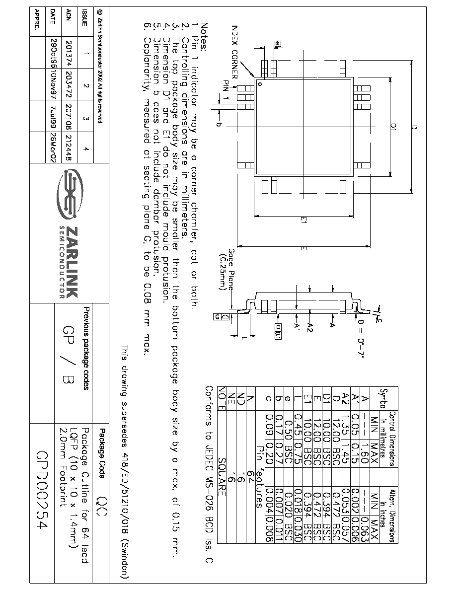


www.zarlink.com
Information relating to products and services furnished herein by Zarlink Semiconductor Inc. trading as Zarlink Semiconductor or its subsidiaries (collectively
"Zarlink") is believed to be reliable. However, Zarlink assumes no liability for errors that may appear in this publication, or for liability otherwise arising from the
application or use of any such information, product or service or for any infringement of patents or other intellectual property rights owned by third parties which may
result from such application or use. Neither the supply of such information or purchase of product or service conveys any license, either express or implied, under
patents or other intellectual property rights owned by Zarlink or licensed from third parties by Zarlink, whatsoever. Purchasers of products are also hereby notified
that the use of product in certain ways or in combination with Zarlink, or non-Zarlink furnished goods or services may infringe patents or other intellectual property
rights owned by Zarlink.
This publication is issued to provide information only and (unless agreed by Zarlink in writing) may not be used, applied or reproduced for any purpose nor form part
of any order or contract nor to be regarded as a representation relating to the products or services concerned. The products, their specifications, services and other
information appearing in this publication are subject to change by Zarlink without notice. No warranty or guarantee express or implied is made regarding the
capability, performance or suitability of any product or service. Information concerning possible methods of use is provided as a guide only and does not constitute
any guarantee that such methods of use will be satisfactory in a specific piece of equipment. It is the user's responsibility to fully determine the performance and
suitability of any equipment using such information and to ensure that any publication or data used is up to date and has not been superseded. Manufacturing does
not necessarily include testing of all functions or parameters. These products are not suitable for use in any medical products whose failure to perform may result in
significant injury or death to the user. All products and materials are sold and services provided subject to Zarlink's conditions of sale which are available on request.
Purchase of Zarlink's I
2
C components conveys a licence under the Philips I
2
C Patent rights to use these components in an I
2
C System, provided that the system
conforms to the I
2
C Standard Specification as defined by Philips.
Zarlink, ZL and the Zarlink Semiconductor logo are trademarks of Zarlink Semiconductor Inc.
Copyright 2003, Zarlink Semiconductor Inc. All Rights Reserved.
TECHNICAL DOCUMENTATION - NOT FOR RESALE
For more information about all Zarlink products
visit our Web Site at