DS3605-2.2
The GP1020 is a six-channel CMOS digital correlator which
has been designed to work with the GP1010 L1-channel down-
converter or other integrated circuits, and may be used to acquire
and track the GPS C/A code or the GLONASS signals.
For each of the six channels the GP1020 includes independ-
ent digital down-conversion to baseband, C/A code generation,
correlation, and accumulate-and-dump registers.
The GP1020 interfaces with a microprocessor via a 16-bit
data bus to control the acquisition and tracking processes using
the various registers on the chip.
FEATURES
s
Six Fully Independent Correlation Channels
s
Switchable to Receive GPS or GLONASS Codes
s
Input Multiplexer for Multiple GPS Front-Ends ≠ Allows
Antenna Diversity
s
Input Multiplexer for GLONASS Multiple (Separate
Channels) Front-Ends
s
Digital Interface Compatible with Most 16 or 32-Bit
Microprocessors
s
Fully Compatible with GP1010 GPS Receiver Front-End
s
Sideways Stackable to give Multiples of Six Channels
s
120-pin Plastic Quad Flatpack
s
Power Dissipation Less Than 500mW
APPLICATIONS
s
GPS or GLONASS Navigation Systems
s
High Integrity Combined Receivers
s
GPS Geodetic Receivers
s
GPS Time Reference
ORDERING INFORMATION
The GP1020 is available in 120-pin Quad Flatpacks (Gullwing
formed leads) in both Commercial (0
∞
C to 170
∞
C) and Industrial
(240
∞
C to 185
∞
C) grades. The ordering codes below are for
standard screened devices.
ORDERING CODES
GP1020 CG GPKR Commercial - Plastic 120-pin QFP (GP120)
GP1020 IG GPKR Industrial - Plastic 120-pin QFP (GP120)
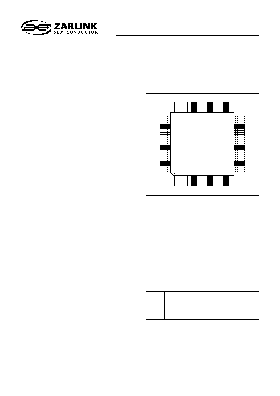
GP
1020
91
120
61
90
1
30
31
60
GP120
Fig 1 Pin connections - top view
ABSOLUTE MAXIMUM RATINGS
These are not the operating conditions, but are the absolute
limits which if exceeded, even momentarily, may cause perma-
nent damage. To ensure sustained correct operation the device
should be used within the limits given under Electrical Character-
istics.
Supply voltage (V
DD
) from ground (V
SS
):
2
0∑3V to16∑0 V
Input voltage (any input pin):
V
SS
2
0∑3V to V
DD
1
0∑3 V
Output voltage (any output pin): V
SS
2
0∑3V to V
DD
1
0∑3 V
Storage temperature:
2
55
∞
C to 1125
∞
C
RELATED PRODUCTS
Description
35∑42MHz SAW Filter
GPS Receiver Front-End
Part
DW9255
GP1010
Datasheet
Reference
DS3861
DS3076
GP1020
SIX-CHANNEL PARALLEL CORRELATOR CIRCUIT
FOR GPS OR GLONASS RECEIVERS
FEBRUARY 1994
2
GP1020
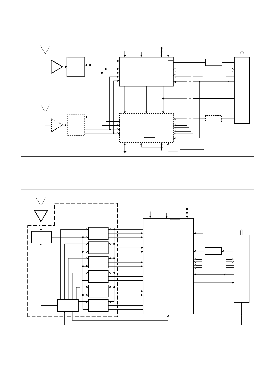
TYPICAL GPS RECEIVER (Fig. 2)
All satellites use the same L1 frequency of 1575∑42MHz, but different Gold codes, so a single front-end may be used. To
achieve better sky coverage it may be desirable to use more than one antenna, in which case separate front-ends will be needed.
TYPICAL GLONASS RECEIVER (Fig. 3)
Each satellite will use a different `L1' carrier frequency, in the range 1602∑5625 to 1615∑500MHz, with 0∑5625MHz spacing,
but all with the same 511-bit spreading code. The normal method for receiving these signals is to use several front-ends, perhaps
with the first LNA and mixer common, but certainly with different final local oscillators and mixers.
Fig. 3 GLONASS receiver simplified block diagram
Fig. 2 GPS receiver simplified block diagram
GP1020
(MASTER)
SIGN 0
MAG 0
SIGN 1
MAG 1
OPTIONAL SECOND
GP1020
(SLAVE)
V
DD
GND
MASTERRESET
SIGN 0
MAG 0
SIGN 1
MAG 1
V
DD
GND
MASTERRESET
DATA BUS (16)
ADDR BUS (8)
MASTER/SLAVE
1
5V
MASTER/SLAVE
V
SS
V
SS
SLAVECLK
TIC OUT
TIC IN
INT OUT
INT IN
1
5V
DECODE
DECODE
MICROPROCESSOR
SYSTEM
MASTER CLK
SAMPLE CLK
SIGN
MAG
GP1010
&
FILTER
OPTIONAL
SECOND
GP1010
&
FILTER
CS
CS
MULTIPLE ANTENNAS TO GIVE
WIDER SKY COVERAGE
CONTROL
3
NAVIGATION
SOLUTION
V
DD
GND
MASTER/SLAVE
V
SS
1
5V
GP1020
MASTERRESET
DATA BUS (16)
ADDR BUS (8)
DECODE
MICROPROCESSOR
SYSTEM
OSCILLATOR
FREQUENCY
SELECTION
INT OUT
SAMPLE CLK
SIGN
MAG
CHANNEL
SELECTION
AND ADC
SIGN
MAG
CHANNEL
SELECTION
AND ADC
CHANNEL
SELECTION
AND ADC
SIGN
MAG
CHANNEL
SELECTION
AND ADC
SIGN
MAG
CHANNEL
SELECTION
AND ADC
SIGN
MAG
CHANNEL
SELECTION
AND ADC
SIGN
MAG
CHANNEL
SELECTION
AND ADC
FREQUENCY
GENERATOR
SAMP CLK
SIGN 0
MAG 0
SIGN 1
MAG 1
SIGN 2
MAG 2
SIGN 3
MAG 3
SIGN 4
MAG 4
SIGN 5
MAG 5
L-BAND
DOWN
CONVERTER
CS
MASTER
CLOCK
GLONASS FRONT-END
FILTERS, AMPLIFIERS
AND MIXERS
CONTROL 3
NAVIGATION
SOLUTION
GP1020
3
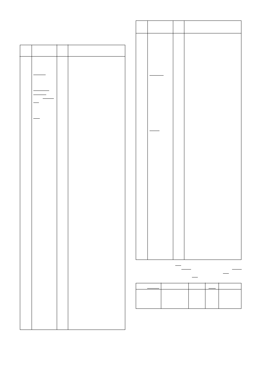
PIN DESCRIPTIONS (See Application Notes, p. 41)
All V
SS
and all V
DD
pins must be used in order to ensure
reliable operation. Several pins, such as Satellite Inputs 2 to
9 Sign and Magnitudes are also used for device testing, but
only as a secondary function.
Description
Type
Register Address, bit 7
Register Address, bit 8
Master or slave mode select
Scan Test mode select
Test Clock select
Serial Test Data Input
Master Reset (active low)
Motorola (hi) or Intel (lo) bus select
Chip Select (active low) for bus
Ground
Positive supply
Bus control - see note 1
Bus control - see note 1
Test Mode Select 2
Test Mode Select 1
Test PRN Pattern Magnitude o/p
Test PRN Pattern Sign output
Satellite Input 2, Magnitude
Programmable Interrupt Timer clock
Positive supply
Ground
Interrupt out to microprocessor
Satellite Input 2, Sign
Satellite Input 3, Magnitude
Satellite Input 3, Sign
Satellite Input 4, Magnitude
Satellite Input 4, Sign
Satellite Input 5, Magnitude
Satellite Input 5, Sign
Satellite Input 6, Magnitude
Satellite Input 6, Sign
Satellite Input 7, Magnitude
Satellite Input 7, Sign
Satellite Input 8, Magnitude
Satellite Input 8, Sign
Satellite Input 9, Magnitude
Satellite Input 9, Sign
Satellite Input 1, Magnitude
Satellite Input 1, Sign
Ground
Positive supply
Satellite Input 0, Magnitude
Satellite Input 0, Sign
Sampling clock to down-converter
Positive supply
40MHz Master Clock
Ground
Bias for MASTERCLK in 600mV
AC-coupled mode
Ground
Positive supply
Ground
Sets 100/219kHz to 100or 219kHz
PLL lock status from down-converter
BITE control to down-converter
I/P to monitor GLONASS front-end
20MHz clock from Master to slave
Interrupt to slave to sync to Master
Test Clock 1
Test Clock 2
Test Clock 3
Test Clock 4
Test Clock 5
Test Clock 6
Test Clock 7
Test Clock 8
Pin
No.
1
2
3
4
5
6
7
8
9
10
11
12
13
14
15
16
17
18
19
20
21
22
23
24
25
26
27
28
29
30
31
32
33
34
35
36
37
38
39
40
41
42
43
44
45
46
47
48
49
50
51
52
53
54
55
56
57
58
59
60
61
62
63
64
65
Signal
name
A7
A8
MASTER/
SLAVE
TSCAN
TCKS
TDI1
MASTER
RESET
MOT/INTEL
CS
V
SS
V
DD
WEN
RW
TMS2
TMS1
TMAG
TSIGN
MAG2
100/219kHz
V
DD
V
SS
INTOUT
SIGN2
MAG3
SIGN3
MAG4
SIGN4
MAG5
SIGN5
MAG6
SIGN6
MAG7
SIGN7
MAG8
SIGN8
MAG9
SIGN9
MAG1
SIGN1
V
SS
V
DD
MAG0
SIGN0
SAMPCLK
V
DD
MASTERCLK
V
SS
Bias
V
SS
V
DD
V
SS
CLKSEL
PLLLOCKIN
BITECNTL
GLONASSBIT
SLAVECLK
INTIN
TCK1
TCK2
TCK3
TCK4
TCK5
TCK6
TCK7
TCK8
I
I
I
I
I
I
I
I
I
2
1
I
I
I
I
O
O
I/O
O
1
2
O
I/O
I/O
I/O
I/O
I/O
I/O
I/O
I/O
I/O
I/O
I/O
I/O
I/O
I/O
I/O
I/O
I/O
2
1
I
I
O
1
I
2
O
2
1
2
I
I
O
I
I/O
I
I/O
I/O
I/O
I/O
I/O
I/O
I/O
I
TIC input to slave
TIC output from Master
Data Bus, bit 0
Data Bus, bit 1
Ground
Positive supply
Data Bus, bit 2
Data Bus, bit 3
One pulse per second output
Real time clock interrupt input
Timemark line driver feedback
Timemark line driver feedback
Data Bus, bit 4
Data Bus, bit 5
Positive supply
Ground
Data Bus, bit 6
Data Bus, bit 7
Bus timing mode - see note 2
Test Structure - see note 3
Test Structure - see note 3
Boundary Scan output
Boundary Scan clock
Boundary Scan reset
Test Structure - see note 3
Boundary Scan control
Boundary Scan input
Timemark line driver feedback
Serial Test Data Output 7
On/Off control for LNA by GP1010
Serial Test Data Output 6
Serial Test Data Output 5
Data Bus, bit 8
Data Bus, bit 9
Ground
Positive supply
Data Bus, bit 10
Data Bus, bit 11
Serial Test Data Output 4
Serial Test Data Output 3
Serial Test Data Output 2
Serial Test Data Output 1
Data Bus, bit 12
Data Bus, bit 13
Positive supply
Ground
Data Bus, bit 14
Data Bus, bit 15
Address Latch Enable,
bus control
Register Address, bit 1 (LSB)
Register Address, bit 2
Register Address, bit 3
Register Address, bit 4
Register Address, bit 5
Register Address, bit 6
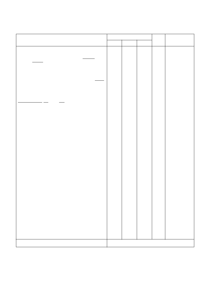
Pin
No.
66
67
68
69
70
71
72
73
74
75
76
77
78
79
80
81
82
83
84
85
86
87
88
89
90
91
92
93
94
95
96
97
98
99
100
101
102
103
104
105
106
107
108
109
110
111
112
113
114
115
116
117
118
119
120
Signal
name
TICIN
TICOUT
D0
D1
V
SS
V
DD
D2
D3
TIME MARK
RTCINT
MARKFB1
MARKFB2
D4
D5
V
DD
V
SS
D6
D7
WPROG
NANDA
NANDB
TDO
TCK
TRST
NANDOP
TMS
TDI
MARKFB3
TDO7
DISCOP
TDO6
TDO5
D8
D9
V
SS
V
DD
D10
D11
TDO4
TDO3
TDO2
TDO1
D12
D13
V
DD
V
SS
D14
D15
ALE
A1
A2
A3
A4
A5
A6
Description
Type
I
O
I/O
I/O
2
1
I/O
I/O
O
I
I
I
I/O
I/O
1
2
I/O
I/O
I
I
I
O
I
I
O
I
I
I
O
O
O
O
I/O
I/O
2
1
I/O
I/O
O
O
O
O
I/O
I/O
1
2
I/O
I/O
I
I
I
I
I
I
I
MOT/INTEL
1
1
0
0
WEN
1
1
1
0
RW
0
1
0
1
Mode
Motorola
Motorola
Intel
Intel
Function
Write
Read
Read
Write
NOTE 1. The functions of RW and WEN pins depend on whether the
GP1020 is in MotorolaTM (MOT/INTEL = `1') or IntelTM mode (MOT/INTEL
= `0'). In Motorola mode, WEN is an enable (active high) and RW is Read/
Write select (`1' = Read). In Intel mode RW is Read, active low, and WEN
is Write, also active low.
NOTE 2. WPROG is used to modify the timing of bus operations; when it
is held HIGH the internal write signal is ORed with ALE to allow time for the
internal address lines to stabilise; when it is held LOW there is no delay
added to write. NOTE 3. NANDOP (pin 90) is the output of a spare gate with
inputs on NANDA (pin 85) and NANDB (pin 86).
4
GP1020
mA
V
V
k
V
V
k
V
V
µ
A
V
V
k
V
V
k
mV
V
V
V
V
V
V
µ
A
V
V
µ
A
V
V
µ
A
75
75
1
75
75
V
DD
2
0∑5
0∑2
V
DD
2
0∑5
0∑2
V
DD
2
0∑5
0∑2
V
DD
2
0∑5
0∑2
V
DD
2
0∑5
0∑2
ELECTRICAL CHARACTERISTICS
These characteristics are guaranteed over the following conditions (unless otherwise stated):
Supply voltage, V
DD
= 5V
±
10%; Ambient Temperature, T
AMB
= 0
∞
C to 170
∞
C (CG grade),240
∞
C to 185
∞
C (IG grade).
DC CHARACTERISTICS
Supply current, I
DD
, chip fully active
CMOS inputs with pullup resistors to V
DD
: RTCINT,
MASTER/SLAVE, MARKFB (3:1), NANDA, NANDB,
WPROG, ALE
Input voltage high
Input voltage low
Pullup resistor
CMOS inputs with pulldown resistors to V
SS
: MOT/INTEL,
CLKSEL, INT IN, TIC IN
Input voltage high
Input voltage low
Pulldown resistor
CMOS inputs without either pullup or pulldown resistors:
MASTERRESET, CS, WEN, RW, MASTERCLK (note 1),
SLAVECLK, A (8:1), D (15:0), TCK, TDI, TMS, TRST
Input voltage high
Input voltage low
Input leakage current
TTL inputs with pullup resistors to V
DD
: SIGN (9:0),
MAG (9:0), PLLLOCKIN, GLONASSBIT
Input voltage high
Input voltage low
Pullup resistor
TTL inputs with pulldown resistors to V
SS
: TSCAN, TCKS,
TDI1, TMS1, TMS2
Input voltage high
Input voltage low
Pulldown resistor
Input for low level clocks: MASTERCLK (note 1)
Peak to peak sinewave
Power level 1 outputs: TMAG, TSIGN, TDO, TDO (7:1),
NANDOP
Output voltage high
Output voltage low
Power level 3 outputs: 100/219kHz, INT OUT, SAMPCLK,
TIC OUT, BITE CNTL, DISCOP, TIMEMARK
Output voltage high
Output voltage low
Power level 1 outputs with tri-state: MAG (9:2), SIGN (8:2),
TCK (7:1)
Output voltage high
Output voltage low
Output leakage current
Power level 3 output with tri-state: SLAVECLK
Output voltage high
Output voltage low
Output leakage current
Power level 6 output with tri-state: D (15:0)
Output voltage high
Output voltage low
Output leakage current
Bias output: BIAS
Units
Conditions
Max.
Typ.
0∑8V
DD
20
0∑8V
DD
20
0∑8V
DD
2∑0
20
2∑0
20
600
V
DD
2
1
V
DD
2
1
V
DD
2
1
V
DD
2
1
V
DD
2
1
Min.
Value
Characteristic
100
0∑2V
DD
250
0∑2V
DD
250
0∑2V
DD
10
0∑8
250
0∑8
250
0∑4
0∑4
0∑4
10
0∑4
10
0∑4
10
V
SS
<V
PIN
<V
DD
AC coupled
I
OH
= 21∑5mA
I
OL
= 1∑5mA
I
OH
= 24∑5mA
I
OL
= 4∑5mA
I
OH
= 21∑5mA
I
OL
= 1∑5mA
V
SS
<V
PIN
<V
DD
I
OH
= 24∑5mA
I
OL
= 4∑5mA
V
SS
<V
PIN
<V
DD
I
OH
= 29∑0mA
I
OL
= 9∑0mA
V
SS
<V
PIN
<V
DD
Special output to be used only as shown in Fig. 12 (page 8)
NOTE 1.
The input MASTERCLK may be driven by either CMOS logic levels or by a low amplitude sinewave if the BIAS pin is connected as shown
in Fig. 12.
GP1020
5
Address hold time
ALE pulse width
ALE valid to WEN or RW valid (WPROG = 1)
ALE valid to WEN or RW valid (WPROG = 0)
Address valid to ALE low
Address valid to WEN or RW valid
CS high to ALE valid
CS low to WEN or RW valid
Data hold time
Data setup time
RW high to data at high impedance
RW valid to data valid
RW valid to WEN high
WEN low to RW not valid
Write pulse width
CS hold time after RW or WEN not valid
25
50
ns
ns
ns
ns
ns
ns
ns
ns
ns
ns
ns
ns
ns
ns
ns
ns
Max.
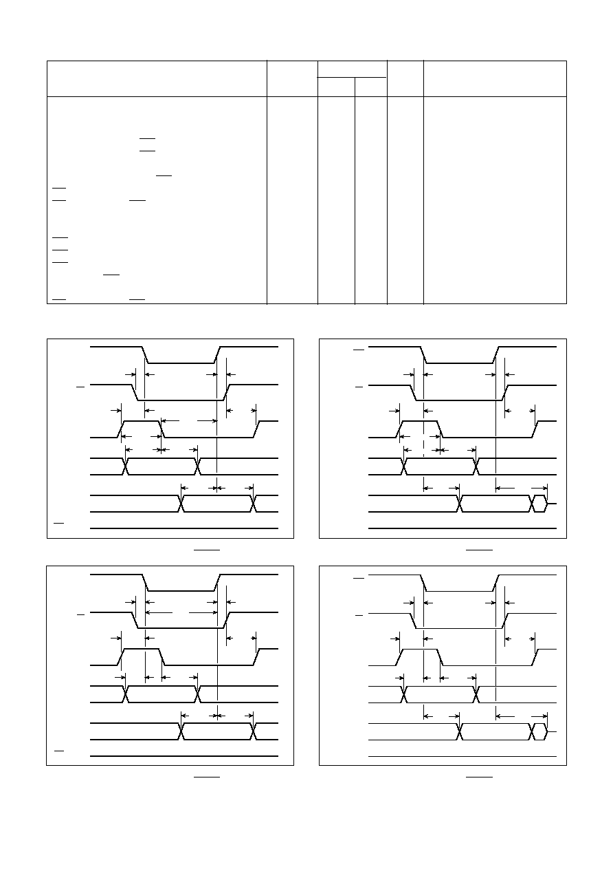
TIMING CHARACTERISTICS (See Figs. 4 to 9)
Conditions
Units
Characteristic
Value
10
20
5
20
20
20
10
0
10
30
10
10
15
15
30
0
Min.
Symbol
t
AHOLD
t
ALEPW
t
ALESETUP
t
ALVWRV
t
ASETUP
t
AVWRV
t
CHALV
t
CVWRV
t
DHOLD
t
DSETUP
t
RHDZ
t
RVDV
t
RWVWENH
t
WENLRWNV
t
WLWH
t
WRCH
NOTE. This timing information is based on simulations and is not verified by measurement on each device.
GP1020 BUS TIMING DIAGRAMS
WEN
CS
ALE
A (8:1)
D (15:0)
RW (HIGH)
t
ALESETUP
t
ASETUP
t
AHOLD
ADDRESS VALID
t
ALEPW
t
CVWRV
DATA VALID
t
DSETUP
t
DHOLD
NEXT
R/W
t
WRHCH
t
CHALV
t
WLWH
Fig. 4 Intel 486 mode WRITE. MOT/INTEL = 0, WPROG = 1
(Write inhibited until ALE falling edge)
Fig. 5 Intel 486 mode READ. MOT/INTEL = 0, WPROG = 1
Fig. 6 Intel 186 mode WRITE. MOT/INTEL = 0, WPROG = 0
WEN
CS
ALE
A (8:1)
D (15:0)
RW (HIGH)
t
ALVWRV
t
AHOLD
ADDRESS VALID
t
AVWRV
t
CVWRV
DATA VALID
t
DSETUP
t
DHOLD
NEXT
R/W
t
WRHCH
t
CHALV
t
WLWH
Fig. 7 Intel 186 mode READ. MOT/INTEL = 0, WPROG = 0
RW
CS
ALE
A (8:1)
D (15:0)
WEN (HIGH)
t
ALESETUP
t
ASETUP
t
AHOLD
ADDRESS VALID
t
ALEPW
t
CVWRV
DATA VALID
t
RVDV
t
RHDZ
NEXT
R/W
t
WRHCH
t
CHALV
RW
CS
ALE
A (8:1)
D (15:0)
WEN (HIGH)
t
ALVWRV
t
AVWRV
t
AHOLD
ADDRESS VALID
t
CVWRV
DATA VALID
t
RVDV
t
RHDZ
NEXT
R/W
t
WRHCH
t
CHALV