1
Features
∑
3.3 volt supply
∑
5V tolerant inputs and TTL compatible outputs
∑
256 x 256 channel non-blocking switch
∑
Programmable frame integrity for wideband
channels
∑
Automatic identification of ST-BUS/GCI
interface backplanes
∑
Per channel tristate control
∑
Patented message mode
∑
Non-multiplexed microprocessor interface
∑
Available in PLCC-44 and SSOP-48 packages
∑
Pin compatible with MT8985 device
∑
Low power consumption
Applications
∑
Medium size digital switch matrices
∑
Hyperchannel switching (e.g., ISDN H0)
∑
ST-BUS/MVIP
TM
interface functions
∑
Serial bus control and monitoring
∑
Centralized voice processing systems
∑
Data multiplexer
Description
The MT89L85 Enhanced Digital Switch device is an
upgraded 3-volt version of the MT8985 Digital
Switch. It is pin compatible with the MT8985 and
retains all of the MT8985's functionality. The
enhanced digital swtich is designed for switching
PCM-encoded voice or data, under microprocessor
control, in digital exchanges, PBXs and any ST-BUS/
MVIP environment. It provides simultaneous
connections for up to 256 64kb/s channels. Each of
the eight serial inputs and outputs consist of 32 64
kbit/s channels multiplexed to form a 2048 kbit/s
stream. As the main function in switching
applications, the device provides per-channel
selection between variable or constant throughput
delays. The constant throughput delay feature allows
grouped channels such as ISDN H0 to be switched
through the device maintaining its sequence
integrity. The MT89L85 is ideal for medium sized
mixed voice/data switch and voice processing
applications.
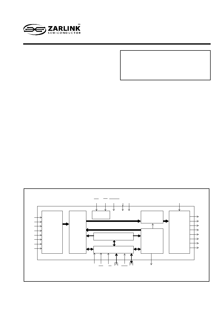
Figure 1 - Functional Block Diagram
STo0
STo1
STo2
STo3
STo4
STo5
STo6
STo7
Serial
to
Parallel
Converter
Data
Memory
Frame
Counter
Control Register
Control Interface
Output
MUX
Connection
Memory
Parallel
to
Serial
Converter
CS R/W A5/
A0
DTA D7/
D0
CSTo
C4i
F0i
ODE
STi0
STi1
STi2
STi3
STi4
STi5
STi6
STi7
DS
DS5194
ISSUE 2
September 1999
MT89L85
Enhanced Digital Switch
CMOS ST-BUS
TM FAMILY
Ordering Information
MT89L85AP
44 Pin PLCC
MT89L85AN
48 Pin SSOP
-40
C to +85C
Advance Information
RESET
** for 48-pin SSOP only
V
DD
V
SS
**

MT89L85
Advance Information
2
Figure 2 - Pin Connections
Pin Description
Pin #
Name
Description
44
PLCC
48
SSOP
2
2
DTA
Data Acknowledgment (Open Drain Output). This active low output indicates that a
data bus transfer is complete. A pull-up resistor is required at this output.
3-5
7-11
3-5
7-11
STi0-
STi7
ST-BUS Input 0 to 7 (Inputs). Serial data input streams. These streams have 32
channels at data rates of 2.048 Mbit/s.
12
12,36
V
DD
+3.3 Volt Power Supply.
13
RESET Device Reset (5v-tolerant input). This pin is only available for the 48-pin SSOP
package. This active low input puts the MT89L85 in its reset state. It clears the internal
counters anf registers. All ST-BUS outputs are set to the high impedance state. This
RESET pin must be held low for a minimum of 100nsec to reset the device.
13
14
F0i
Frame Pulse (Input). This input accepts and automatically identifies frame
synchronization signals formatted according to different backplane specifications such
as ST-BUS and GCI.
14
15
C4i
Clock (Input). 4.096 MHz serial clock for shifting data in and out of the data streams.
15-17
19-21
16-18
20-22
A0-A5 Address 0 to 5 (Inputs). These lines provide the address to MT89L85 internal
registers.
22
23
DS
Data Strobe (Input). This is the input for the active high data strobe on the
microprocessor interface. This input operates with CS to enable the internal read and
write generation.
(JEDEC MO-118, 300mil Wide)
1
6
5
4
3
2
44
43
42
41
40
7
8
9
10
11
12
13
14
15
16
39
38
37
36
35
34
33
32
31
30
23
18
19
20
21
22
24
25
26
27
28
17
29
STi3
STi4
STi5
STi6
STi7
V
DD
F0i
C4i
A0
A1
A2
STo3
STo4
STo5
STo6
STo7
V
SS
D0
D1
D2
D3
D4
NC
STi1
DTA
ODE
STo1
NC
NC
A4
DS
CS
D6
NC
A3
A5
R/
W
D7
D5
44 PIN PLCC
STi2
STi0
CSTo
STo0
STo2
2
3
4
5
6
7
8
9
10
11
12
13
14
15
16
17
18
19
20
1
48 PIN SSOP
47
46
45
44
43
42
41
40
39
38
37
36
35
34
33
32
31
30
29
28
ODE
STo0
STo1
STo2
NC
STo3
STo4
STo5
STo6
STo7
V
SS
V
DD
D0
D1
D2
D3
D4
NC
D5
D6
DTA
STi0
STi1
STi2
NC
STi3
STi4
STi5
STi6
STi7
V
DD
RESET
F0i
C4i
A0
A1
A2
NC
A3
A4
48
CSTo
V
SS
21
27
D7
A5
22
26
CS
DS
23
25
V
SS
R/W
24

Advance Information
MT89L85
3
23
24
R/W
Read/Write (Input). This input controls the direction of the data bus lines (D0-D7)
during a microprocessor access.
24
26
CS
Chip Select (Input). Active low input enabling a microprocessor read or write of
control register or internal memories.
25-27
29-33
27-29
31-35
D7-D0
Data Bus 7 to 0 (Bidirectional). These pins provide microprocessor access to data in
the internal control register, connect memory high, connect memory low and data
memory.
34
1,25,37
V
SS
Ground Rail.
35-39
41-43
38-42
44-46
STo7-
STo0
ST-BUS Outputs 7 to 0 (Three-state Outputs). Serial data output streams. These
streams are composed of 32 channels at data rates of 2.048 Mbit/s.
44
47
ODE
Output Drive Enable (Input). This is an output enable for the STo0 to STo7 serial
outputs. If this input is low STo0-7 are high impedance. If this input is high each
channel may still be put into high impedance by software control.
1
48
CSTo
Control ST-BUS Output (Output). This output is a 2.048 Mb/s line which contains 256
bits per frame. The level of each bit is controlled by the contents of the CSTo bit in the
Connect Memory high locations.
6,18,
28,40
6,19,30,
43
NC
No Connection.
Pin Description
Pin #
Name
Description
44
PLCC
48
SSOP
Functional Description
With the integration of voice, video and data services
into the same network, there has been an increasing
demand for systems which ensure that data at N x 64
Kbit/s rates maintain frame sequence integrity while
being transported through time slot interchange
circuits. Existing requirements demand time slot
interchange devices performing switching with
constant throughput delay while guaranteeing
minimum delay for voice channels.
The MT89L85 device provides both functions and
allows existing systems based on the MT8985 to be
easily upgraded to maintain the data integrity while
multiple channel data are transported. The device is
designed to switch 64 kbit/s PCM or N x 64 kbit/s
data. The MT89L85 can provide both frame integrity
for data applications and minimum throughput
switching delay for voice applications on a per
channel basis.
microprocessor can access input and output time
slots on a per channel basis to control devices such
CEPT trunk interfaces through the ST-BUS interface.
Different digital backplanes can be accepted by the
MT89L85 device without user's intervention. The
MT89L85 device provides an internal circuit that
automatically identifies the polarity and format of
frame synchronization input signals compatible to
ST-BUS and GCI interfaces.
Device Operation
A functional block diagram of the MT89L85 device is
shown in Figure 1. The serial ST-BUS streams
operate continuously at 2.048 Mb/s and are arranged
in 125
µs wide frames each containing 32 8-bit
channels. Eight input (STi0-7) and eight output
(STo0-7) serial streams are provided in the MT89L85
device allowing a complete 256 x 256 channel non-
blocking switch matrix to be constructed. The serial
interface clock for the device is 4.096 MHz, as
required in ST-BUS and GCI specifications.
Data Memory
The received serial data is converted to parallel
format by the on-chip serial to parallel converters
and stored sequentially in a 256-position Data
Memory. The sequential addressing of the Data
Memory is generated by an internal counter that is
reset by the input 8 kHz frame pulse (F0i) marking
the frame boundaries of the incoming serial data
streams.
Depending on the type of information to be switched,
the MT89L85 device can be programmed to perform
By using Zarlink Message mode capability, the
as the Zarlink MT8972, ISDN Transceivers and T1/

MT89L85
Advance Information
2-4
time slot interchange functions with different
throughput delay capabilities on a per-channel basis.
For voice applications, the variable delay mode can
be selected ensuring minimum throughput delay
between input and output data. In multiple or
grouped channel data applications, the constant
delay mode can be selected maintaining the integrity
of the information through the switch.
Data to be output on the serial streams may come
from two sources: Data Memory or Connect Memory.
Locations in the Connect Memory, which is split into
HIGH and LOW parts, are associated with particular
ST-BUS output streams. When a channel is due to
be transmitted on an ST-BUS output, the data for the
channel can either be switched from an ST-BUS
input (connection mode) or it can be originated from
the microprocessor (message mode). If a channel is
configured in connection mode, the source of the
output data is the Data Memory. If a channel is
configured in message mode, the source of the
output data is the Connect Memory Low. Data
destined for a particular channel on the serial output
stream is read from the Data or Connect Memory
Low during the previous channel time slot. This
allows enough time for memory access and internal
parallel to serial conversion.
Connection and Message Modes
In connection mode, the addresses of input source
for all output channels are stored in the Connect
memory Low. The Connect Memory Low locations
are mapped to each location corresponding to an
output 64 kb/s channel. The contents of the Data
memory at the selected address are then transferred
to the parallel to serial converters. By having the
output channel to specify the input channel through
the connect memory, the user can route the same
input channel to several output channels, allowing
broadcasting facility in the switch.
In message mode the CPU writes data to the
Connect Memory Low locations which correspond to
the output link and channel number. The contents of
the Connect Memory Low are transferred to the
parallel to serial converter one channel before it is to
be output. The Connect Memory Low data is
transmitted each frame to the output until it is
changed by the CPU.
The per-channel functions available in the MT89L85
are controlled by the Connect Memory High bits,
which determine whether individual output channels
are selected into specific conditions such as:
message or connection mode, variable or constant
throughput delay modes, output drivers enabled or in
three-state condition. In addition, the Connect
Memory High provides one bit to allow the user to
control the state of the CSTo output pin.
If an output channel is set to three-state condition,
the TDM serial stream output will be placed in high
impedance during that channel time. In addition to
the per-channel three-state control, all channels on
the TDM outputs can be placed in high impedance at
one time by pulling the ODE input pin in LOW. This
overrides the individual per-channel programming on
the Connect Memory High bits.
The Connect Memory data is received via the
Microprocessor Interface at D0-D7 lines. The
addressing of the MT89L85 internal registers, Data
and Connect memories is performed through
address input pins and some bits of the device's
Control register. The higher order address bits come
from the Control register, which may be written or
read through the microprocessor interface. The lower
order address bits come directly from the external
address line inputs. For details on the device
addressing, see Software Control and Control
register description.
Serial Interface Timing
The MT89L85 master clock (C4i) is a 4.096 MHz
allowing serial data link configuration at 2.048 Mb/s
to be implemented. The MT89L85 frame
synchronization pulse can be formatted according to
ST-BUS or GCI interface specifications; i.e., the
frame pulse can be active in HIGH (GCI) or LOW
(ST-BUS). The MT89L85 device automatically
detects the presence of an input frame pulse and
identifies the type of backplane present on the serial
interface. Upon determining the correct interface
connected to the serial port, the internal timing unit
establishes the appropriate serial data bit transmit
and sampling edges. In ST-BUS mode, every second
falling edge of the 4.096 MHz clock marks a bit
boundary and the input data is clocked in by the
rising edge, three quarters of the way into the bit cell.
In GCI mode, every second rising edge of the 4.096
MHz clock marks the bit boundary while data
sampling is performed during the falling edge, at
three quarters of the bit boundaries.
Delay through the MT89L85
The transfer of information from the input serial
streams to the output serial streams results in a
delay through the MT89L85 device. The delay
through the device varies according to the mode
selected in the V/C bit of the connect memory high.

Advance Information
MT89L85
2-5
Variable Delay mode
The delay in this mode is dependent only on the
combination of source and destination channels and
it is not dependent on the input and output streams.
The minimum delay achievable in the MT89L85
device is 3 time slots. In the MT89L85 device, the
information that is to be output in the same channel
position as the information is input (position n),
relative to frame pulse, will be output in the following
frame (channel n, frame n+1). The same occurs if
the input channel has to be output in the two
channels succeeding (n+1 and n+2) the channel
position as the information is input.
The information switched to the third timeslot after
the input has entered the device (for instance, input
channel 0 to output channel 3 or input channel 30 to
output channel 1), is always output three channels
later.
Any switching configuration that provides three or
more timeslots between input and output channels,
will have a throughput delay equal to the difference
between the output and input channels; i.e., the
throughput delay will be less than one frame. Table 1
shows the possible delays for the MT89L85 device in
Variable Delay mode:
Table 1 - Channel Delay for the Variable Delay
Mode
Constant Delay Mode
In this mode frame integrity is maintained in all
switching configurations by making use of a multiple
Data-Memory buffer technique where input channels
written in any of the buffers during frame N will be
read out during frame N+2. In the MT89L85, the
minimum throughput delay achieve-able in Constant
Delay mode will be 32 time slots; for example, when
input time slot 32 (channel 31) is switched to output
time slot 1 (channel 0). Likewise, the maximum delay
is achieved when the first time slot in a frame
(channel 0) is switched to the last time slot in the
frame (channel 31), resulting in 94 time slots of
delay.
Input
Channel
Output
Channel
Throughput Delay
n
m=n, n+1 or
n+2
m-n + 32 timeslots
n
m>n+2
m-n time slots
n
m<n
32-(n-m) time slots
To summarize, any input time slot from input frame N
will be always switched to the destination time slot on
output frame N+2. In Constant Delay mode, the
device throughput delay is calculated according to
the following formula:
DELAY = [32 + (32 - IN) + (OUT - 1)];
(expressed in number of time slots)
Where:
IN is the number of the input time slot
(from 1 to 32).
OUT is the number of the output time slot
(from 1 to 32).
Microprocessor Port
The MT89L85 microprocessor port has pin
devices providing a non-multiplexed bus architecture.
The parallel port consists of an 8 bit parallel data bus
(D0-D7), six address input lines (A0-A5) and four
control lines (CS, DS, R/W and DTA). This parallel
microport allows the access to the Control registers,
Connection Memory High, Connection Memory Low
and the Data Memory. All locations are read/written
except for the data memory which can be read only.
Accesses from the microport to the connection
memory and the data memory are multiplexed with
accesses from the input and output TDM ports. This
can cause variable Data Acknowledge delays (DTA).
Figure 3 - Address Memory Map
Note: "x" Don't care
Software Control
The address lines on the microprocessor interface
give access to the MT89L85 internal registers and
memories. If the A5,A1,A0 address line inputs are
LOW, then the MT89L85 Internal Control Register is
addressed (see Figure 3). If A5 input line is HIGH,
then the remaining address input lines are used to
select Memory subsections of 32 locations
corresponding to the number of channels per input or
output stream. As explained in the Control register
A5
A4
A3
A2
A1
A0
LOCATION
0
1
1
1
1
1
1
1
1
0
0
0
∑
∑
∑
∑
∑
1
0
0
0
∑
∑
∑
∑
∑
1
0
0
0
∑
∑
∑
∑
∑
1
0
0
0
∑
∑
∑
∑
∑
1
0
0
1
∑
∑
∑
∑
∑
1
Control Register
Channel 0
Channel 1
∑
∑
∑
∑
∑
Channel 31
compatibility with Zarlink MT8985 Digital Switch