
1
Figure 1 - Functional Block Diagram
Virtual
Refer-
ence
Selected
Refer-
ence
Master
Clock
Reference
Select
Feedback
TIE
Corrector
Enable
Automatic/Manual
Control State Machine
DPLL
State
Select
State
Select
Guard Time
Circuit
Frequency
Select
MUX
Input
Impairment
Monitor
Output
Interface
Circuit
Reference
Select
MUX
TIE
Corrector
Circuit
MS1
MS2
GTo
GTi
FS1
FS2
PRI
SEC
RST
RSEL
LOS1
LOS2
VDD
VSS
TRST
C3o
C1.5o
C2o
C4o
C8o
C16o
F0o
F8o
F16o
OSCo
OSCi
Features
�
Meets jitter requirements for: AT&T TR62411
Stratum 3, 4 and Stratum 4 Enhanced for DS1
interfaces; and for ETSI ETS 300 011, TBR 4,
TBR 12 and TBR 13 for E1 interfaces
�
Provides C1.5, C3, C2, C4, C8 and C16 output
clock signals
�
Provides 8kHz ST-BUS framing signals
�
Selectable 1.544MHz, 2.048MHz or 8kHz input
reference signals
�
Accepts reference inputs from two independent
sources
�
Provides bit error free reference switching -
meets phase slope and MTIE requirements
�
Operates in either Normal, Holdover and
Freerun modes
Applications
�
Synchronization and timing control for
multitrunk T1 and E1 systems
�
ST-BUS clock and frame pulse sources
�
Primary Trunk Rate Converters
Description
The MT9042C Multitrunk System Synchronizer
contains a digital phase-locked loop (DPLL), which
provides timing and synchronization signals for
multitrunk T1 and E1 primary rate transmission links.
The MT9042C generates ST-BUS clock and framing
signals that are phase locked to either a 2.048MHz,
1.544MHz, or 8kHz input reference.
The MT9042C is compliant with AT&T TR62411
Stratum 3, 4 and 4 Enhanced, and ETSI ETS 300
011. It will meet the jitter tolerance, jitter transfer,
intrinsic jitter, frequency accuracy, holdover
accuracy, capture range, phase slope and MTIE
requirements for these specifications.
Ordering Information
MT9042CP
28 Pin PLCC
-40
�
C to +85
�
C
DS5144
ISSUE 3
June 2000
MT9042C
Multitrunk System Synchronizer

MT9042C
2
Figure 2 - Pin Connections
Pin Description
Pin #
Name
Description (see notes 1 to 5)
1,15
V
SS
Ground.
0 Volts.
2
TRST
TIE Circuit Reset (TTL Input).
A logic low at this input resets the Time Interval Error (TIE)
correction circuit resulting in a re-alignment of input phase with output phase as shown in
Figure 19. The TRST pin should be held low for a minimum of 300ns.
3
SEC
Secondary Reference (TTL Input).
This is one of two (PRI & SEC) input reference sources
(falling edge) used for synchronization. One of three possible frequencies (8kHz,
1.544MHzMHz, or 2.048MHz) may be used. The selection of the input reference is based
upon the MS1, MS2, LOS1, LOS2, RSEL, and GTi control inputs (Automatic or Manual).
4
PRI
Primary Reference (TTL Input).
See pin description for SEC.
5,18
V
DD
Positive Supply Voltage.
+5V
DC
nominal.
6
OSCo
Oscillator Master Clock (CMOS Output).
For crystal operation, a 20MHz crystal is
connected from this pin to OSCi, see Figure 10. For clock oscillator operation, this pin is left
unconnected, see Figure 9.
7
OSCi
Oscillator Master Clock (CMOS Input).
For crystal operation, a 20MHz crystal is connected
from this pin to OSCo, see Figure 10. For clock oscillator operation, this pin is connected to a
clock source, see Figure 9.
8
F16o
Frame Pulse ST-BUS 16.384Mb/s (CMOS Output).
This is an 8kHz 61ns active low framing
pulse, which marks the beginning of an ST-BUS frame. This is typically used for ST-BUS
operation at 16.384Mb/s. See Figure 20.
9
F0o
Frame Pulse ST-BUS 2.048Mb/s (CMOS Output).
This is an 8kHz 244ns active low framing
pulse, which marks the beginning of an ST-BUS frame. This is typically used for ST-BUS
operation at 2.048Mb/s and 4.096Mb/s. See Figure 20.
10
F8o
Frame Pulse ST-BUS 8.192Mb/s (CMOS Output).
This is an 8kHz 122ns active high framing
pulse, which marks the beginning of an ST-BUS frame. This is used for ST-BUS operation at
8.192Mb/s. See Figure 20.
11
C1.5o
Clock 1.544MHz (CMOS Output).
This output is used in T1 applications.
12
C3o
Clock 3.088MHz (CMOS Output).
This output is used in T1 applications.
13
C2o
Clock 2.048MHz (CMOS Output).
This output is used for ST-BUS operation at 2.048Mb/s.
14
C4o
Clock 4.096MHz (CMOS Output).
This output is used for ST-BUS operation at 2.048Mb/s
and 4.096Mb/s.
1
6
5
4
3
2
7
8
9
10
11
23
19
20
21
22
24
25
26
27
28
VSS
TRST
SEC
PRI
VDD
OSCo
OSCi
F16o
F0o
F8o
C1.5o
GTi
GTo
LOS2
LOS1
MS2
MS1
RSEL
FS2
FS1
RST
12 13 14 15 16 17 18
C2o
VSS
C8o
C16
o
VDD
C4o
C3o
MT9042C
3
Notes:
1. All inputs are CMOS with either TTL compatible logic levels, CMOS compatible logic levels or Schmitt trigger compatible logic levels
as indicated in the Pin Description.
2. All outputs are CMOS with CMOS compatible logic levels.
3. See DC Electrical Characteristics for static logic threshold values.
4. See AC Electrical Characteristics - Timing Parameter Measurement Voltage Levels for dynamic logic threshold values.
5. Unless otherwise stated, all unused inputs should be connected to logic high or logic low and all unused outputs should be left open
circuit.
16
C8o
Clock 8.192MHz (CMOS Output).
This output is used for ST-BUS operation at 8.192Mb/s.
17
C16o
Clock 16.384MHz (CMOS Output).
This output is used for ST-BUS operation at 16.384Mb/s.
19
GTi
Guard Time (Schmitt Input).
This input is used by the MT9042B state machine in both
Manual and Automatic modes. The signal at this pin affects the state changes between
Primary Holdover Mode and Primary Normal Mode, and Primary Holdover Mode and
Secondary Normal Mode. The logic level at this input is gated in by the rising edge of F8o.
See Tables 4 and 5.
20
GTo
Guard Time (CMOS Output).
The LOS1 input is gated by the rising edge of F8o, buffered
and output on GTo. This pin is typically used to drive the GTi input through an RC circuit.
21
LOS2
Secondary Reference Loss (TTL Input).
This input is normally connected to the loss of
signal (LOS) output signal of a Line Interface Unit (LIU). When high, the SEC reference signal
is lost or invalid. LOS2, along with the LOS1 and GTi inputs control the MT9042B state
machine when operating in Automatic Control. The logic level at this input is gated in by the
rising edge of F8o.
22
LOS1
Primary Reference Loss (TTL Input).
Typically, external equipment applies a logic high to
this input when the PRI reference signal is lost or invalid. The logic level at this input is gated
in by the rising edge of F8o. See LOS2 description.
23
MS2
Mode/Control Select 2 (TTL Input).
This input, in conjunction with MS1, determines the
device's mode (Automatic or Manual) and state (Normal, Holdover or Freerun) of operation.
The logic level at this input is gated in by the rising edge of F8o. See Table 3.
24
MS1
Mode/Control Select 1 (TTL Input).
The logic level at this input is gated in by the rising
edge of F8o. See pin description for MS1.
25
RSEL
Reference Source Select (TTL Input).
In Manual Control, a logic low selects the PRI
(primary) reference source as the input reference signal and a logic high selects the SEC
(secondary) input. In Automatic Control, this pin must be at logic low. The logic level at this
input is gated in by the rising edge of F8o. See Table 2.
26
FS2
Frequency Select 2 (TTL Input).
This input, in conjunction with FS1, selects which of three
possible frequencies (8kHz, 1.544MHz, or 2.048MHz) may be input to the PRI and SEC
inputs. See Table 1.
27
FS1
Frequency Select 1 (TTL Input).
See pin description for FS2.
28
RST
Reset (Schmitt Input).
A logic low at this input resets the MT9042C. To ensure proper
operation, the device must be reset after changes to the method of control, reference signal
frequency changes and power-up. The RST pin should be held low for a minimum of 300ns.
While the RST pin is low, all frame and clock outputs are at logic high. Following a reset, the
input reference source and output clocks and frame pulses are phase aligned as shown in
Figure 19.
Pin Description
Pin #
Name
Description (see notes 1 to 5)
4
MT9042C
Functional Description
The MT9042C is a Multitrunk System Synchronizer,
providing timing (clock) and synchronization (frame)
signals to interface circuits for T1 and E1 Primary
Rate Digital Transmission links.
Figure 1 is a functional block diagram which is
described in the following sections.
Reference Select MUX Circuit
The MT9042C accepts two simultaneous reference
input signals and operates on their falling edges.
Either the primary reference (PRI) signal or the
secondary reference (SEC) signal can be selected
as input to the TIE Corrector Circuit. The selection is
based on the Control, Mode and Reference
Selection of the device. See Tables 1, 4 and 5.
Frequency Select MUX Circuit
The MT9042C operates with one of three possible
input reference frequencies (8kHz, 1.544MHz or
2.048MHz). The frequency select inputs (FS1 and
FS2) determine which of the three frequencies may
be used at the reference inputs (PRI and SEC). Both
inputs must have the same frequency applied to
them. A reset (RST) must be performed after every
frequency select input change. Operation with FS1
and FS2 both at logic low is reserved and must not
be used. See Table 1.
Time Interval Error (TIE) Corrector Circuit
The TIE corrector circuit, when enabled, prevents a
step change in phase on the input reference signals
(PRI or SEC) from causing a step change in phase at
the input of the DPLL block of Figure 1.
During reference input rearrangement, such as
during a switch from the primary reference (PRI) to
the secondary reference (SEC), a step change in
phase on the input signals will occur. A phase step
at the input of the DPLL will lead to unacceptable
phase changes in the output signal.
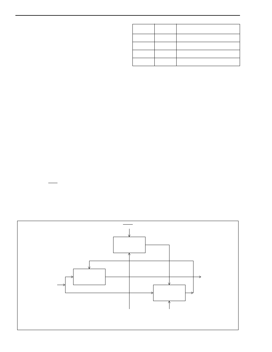
As shown in Figure 3, the TIE Corrector Circuit
receives one of the two reference (PRI or SEC)
signals, passes the signal through a programmable
delay line, and uses this delayed signal as an
internal virtual reference, which is input to the DPLL.
Therefore, the virtual reference is a delayed version
of the selected reference.
During a switch, from one reference to the other, the
State Machine first changes the mode of the device
FS2
FS1
Input Frequency
0
0
Reserved
0
1
8kHz
1
0
1.544MHz
1
1
2.048MHz
Table 1 - Input Frequency Selection
Figure 3 - TIE Corrector Circuit
Programmable
Delay Circuit
Control Signal
Delay Value
TRST
Resets Delay
Compare
Circuit
TIE Corrector
Enable
from
State Machine
Control
Circuit
Feedback
Signal from
Frequency
Select MUX
PRI or SEC
from
Reference
Select Mux
Virtual
Reference
to DPLL

MT9042C
5
from Normal to Holdover. In Holdover Mode, the
DPLL no longer uses the virtual reference signal, but
generates an accurate clock signal using storage
techniques. The Compare Circuit then measures the
phase delay between the current phase (feedback
signal) and the phase of the new reference signal.
This delay value is passed to the Programmable
Delay Circuit (See Figure 3). The new virtual
reference signal is now at the same phase position
as the previous reference signal would have been if
the reference switch not taken place. The State
Machine then returns the device to Normal Mode.
The DPLL now uses the new virtual reference signal,
and since no phase step took place at the input of
the DPLL, no phase step occurs at the output of the
DPLL. In other words, reference switching will not
create a phase change at the input of the DPLL, or at
the output of the DPLL.
Since internal delay circuitry maintains the alignment
between the old virtual reference and the new virtual
reference, a phase error may exist between the
selected input reference signal and the output signal
of the DPLL. This phase error is a function of the
difference in phase between the two input reference
signals during reference rearrangements. Each time
a reference switch is made, the delay between input
signal and output signal will change. The value of
this delay is the accumulation of the error measured
during each reference switch.
The programmable delay circuit can be zeroed by
applying a logic low pulse to the TIE Circuit Reset
(TRST) pin. A minimum reset pulse width is 300ns.
This results in a phase alignment between the input
reference signal and the output signal as shown in
Figure 20. The speed of the phase alignment
correction is limited to 5ns per 125us, and
convergence is in the direction of least phase travel.
The state diagrams of Figure 7 and 8 indicate under
which state changes the TIE Corrector Circuit is
activated.
Digital Phase Lock Loop (DPLL)
As shown in Figure 4, the DPLL of the MT9042C
consists of a Phase Detector, Limiter, Loop Filter,
Digitally Controlled Oscillator, and a Control Circuit.
Phase Detector - the Phase Detector compares the
virtual reference signal from the TIE Corrector circuit
with the feedback signal from the Frequency Select
MUX circuit, and provides an error signal
corresponding to the phase difference between the
two. This error signal is passed to the Limiter circuit.
The Frequency Select MUX allows the proper
feedback signal to be externally selected (e.g., 8kHz,
1.544MHz or 2.048MHz).
Limiter - the Limiter receives the error signal from the
Phase Detector and ensures that the DPLL responds
to all input transient conditions with a maximum
output phase slope of 5ns per 125us. This is well
within the maximum phase slope of 7.6ns per 125us
or 81ns per 1.326ms specified by AT&T TR62411.
Loop Filter - the Loop Filter is similar to a first order
low pass filter with a 1.9 Hz cutoff frequency for all
three reference frequency selections (8kHz,
1.544MHz or 2.048MHz). This filter ensures that the
jitter transfer requirements in ETS 300 011 and AT&T
TR62411 are met.
Control Circuit - the Control Circuit uses status and
control information from the State Machine and the
Input Impairment Circuit to set the mode of the
DPLL. The three possible modes are Normal,
Holdover and Freerun.
Figure 4 - DPLL Block Diagram
Control
Circuit
State Select
from
Input Impairment Monitor
State Select
from
State Machine
Feedback Signal
from
Frequency Select MUX
DPLL Reference
to
Output Interface Circuit
Virtual Reference
from
TIE Corrector
Limiter
Loop Filter
Digitally
Controlled
Oscillator
Phase
Detector