1
Zarlink Semiconductor Inc.
Zarlink, ZL and the Zarlink Semiconductor logo are trademarks of Zarlink Semiconductor Inc.
Copyright 2002-2004, Zarlink Semiconductor Inc. All Rights Reserved.
Features
�
AAL1 Segmentation and Reassembly device
compliant with Circuit Emulation Services (CES)
standard (af-vtoa-0078.000)
�
Supports both Unstructured and Structured
Circuit Emulation of 28 independent DS1/E1/ST-
BUS interfaces
�
Supports AAL1 trunking, with up to 128 TDM
channels per VC (af-vtoa-0089.001)
�
Supports CAS transmission and reception in all
structured modes of operation
�
Supports simultaneous processing of up to 896
bidirectional Virtual Circuits
�
Supports mixed DS1/E1 operation
�
Supports mixed Unstructured and Structured
CES operation
�
Fully flexible DS0 assignment
�
Complete clock recovery solution provided on-
chip: Synchronous, Adaptive, or Synchronous
Residual Time Stamp (SRTS) via 28 independent
PLLs
�
Dual-mode (ATM-end or PHY-end) UTOPIA port
operates in Level 1 or Level 2 mode for
connection to external PHY or ATM devices with
UTOPIA clock rate up to 52 MHz
�
TDM bus provides 28 bidirectional serial streams
at 1.544, 2.048, or 4.096 MHz - compatible with
Generic (1.544 Mbps or 2.048 Mbps) and ST-
BUS (2.048 Mbps) interfaces
�
Supports master and slave TDM backplane bus
clock operation
�
Supports TDM and UTOPIA loopback functions
�
16-bit microprocessor port, configurable to
Motorola or Intel timing
�
Master clock rate of 66.0 MHz
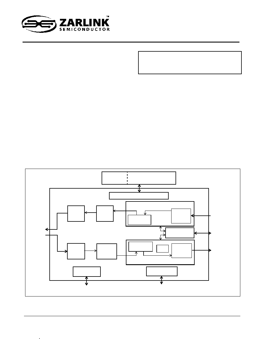
Figure 1 - MT90528 Block Diagram
Segmentation / Reassembly
Circular Buffers
VC Look-Up
Table
External
Synchronous
SRAM (ZBT)
External Memory Controller
UTOPIA
INPUT
BLOCK
JTAG
Interface
16-bit Microprocessor
Interface
Boundary-
Scan Logic
Microprocessor
Interface Logic
UTOPIA
Interface
UTOPIA
OUTPUT
BLOCK
Local
Memory
TDM
INPUT
BLOCK
Tx/Segmentation (X 28)
TX
SAR
Local
Memory
TDM
OUTPUT
BLOCK
RX SARs
(UDT, SDT,
Data)
Rx/Reassembly (X 28)
PLL
Clock
Management
TDM Input
Interface
TDM Output
Interface
MT90528
Clock Control
/Recovery
Interface
January 2004
Ordering Information
MT90528AG
456 Pin Plastic BGA
-40 to +85�C
MT90528
28-Port Primary Rate
Circuit Emulation AAL1 SAR
Data Sheet

MT90528
Data Sheet
2
Zarlink Semiconductor Inc.
Applications
�
B-ISDN (Broadband ISDN) systems requiring flexible N x 64 kbps transport
�
Systems requiring af-vtoa-0078.000 (ATM Forum CES v2.0) "DS1 or E1 Nx64 Basic Service", "DS1 or E1
Nx64 Service with CAS", or "DS1 or E1 Unstructured Service" - flexible CES allows one-board solution to
support multiple CES modes
�
Systems requiring af-vtoa-0089.001 (ATM Forum - ATM Trunking Using AAL1 for Narrowband Services) -
transport of up to 128 channels per VC
�
Ideal for carrier-class WAN access products, especially channelized DS3 or E3 interfaces
�
ATM Edge Switches
�
Carrier Class Voice over ATM systems
�
ATM Public Network access for PBX or CO
�
TDM traffic transfer over an asynchronous cell bus
Description
The MT90528 28-Port Primary Rate Circuit Emulation AAL1 SAR allows primary rate TDM circuits to be carried
over ATM networks using Circuit Emulation Services. Up to 896 bidirectional ATM VC connections can be
simultaneously processed by the MT90528 CES AAL1 SAR device.
The MT90528 supports several modes of Circuit Emulation Services for DS1 and E1 rates. These include
Unstructured CES and Structured CES with and without Channel Associated Signalling (CAS).
On the TDM bus side, the MT90528 interfaces with 28 primary rate TDM ports operating at 1.544 Mbps or
2.048 Mbps. The configurable TDM ports interface directly with DS1 or E1 framers for Nx64 Structured operation,
or with DS1 or E1 LIUs in Unstructured mode.
On the ATM interface side, the MT90528 device meets the ATM Forum standard for UTOPIA Bus Level 2. The
MT90528 is capable of operating as a UTOPIA "master" (ATM-end), "slave" (PHY-end), or "multi-PHY slave" (PHY-
end). The UTOPIA port can operate in 8-bit or 16-bit mode, with a clock rate up to 52 MHz.
Each of the twenty-eight ports of the device contains a PLL, allowing independent timing of each TDM port. Each
PLL supports four modes of clock recovery: SRTS, Adaptive, Synchronous (from the Physical layer), or from the
TDM line clock. Although a complete clock recovery solution is provided internally, an optional external PLL or
external clock source is also supported.
PURCHASE OF THIS PRODUCT DOES NOT GRANT THE PURCHASER ANY RIGHTS UNDER PATENT NO.
5,260,978. USE OF THIS PRODUCT OR ITS RE-SALE AS A COMPONENT OF ANOTHER PRODUCT MAY
REQUIRE A LICENSE UNDER THE PATENT WHICH IS AVAILABLE FROM TELCORDIA TECHNOLOGIES,
INC., 445 SOUTH STREET, MORRISTOWN, NEW JERSEY 07960.
ZARLINK ASSUMES NO RESPONSIBILITY OR LIABILITY THAT MAY RESULT FROM ITS CUSTOMERS' USE
OF ZARLINK PRODUCTS WITH RESPECT TO THIS PATENT. IN PARTICULAR, ZARLINK'S PATENT
INDEMNITY IN ITS TERMS AND CONDITIONS OF SALES WHICH ARE SET OUT IN ITS SALES
ACKNOWLEDGEMENTS AND INVOICES DOES NOT APPLY TO THIS PATENT.

MT90528
Data Sheet
Table of Contents
4
Zarlink Semiconductor Inc.
1.0 Introduction . . . . . . . . . . . . . . . . . . . . . . . . . . . . . . . . . . . . . . . . . . . . . . . . . . . . . . . . . . . . . . . . . . . . . . . . . . 12
1.1 Functional Overview . . . . . . . . . . . . . . . . . . . . . . . . . . . . . . . . . . . . . . . . . . . . . . . . . . . . . . . . . . . . . . . . . 12
2.0 Features . . . . . . . . . . . . . . . . . . . . . . . . . . . . . . . . . . . . . . . . . . . . . . . . . . . . . . . . . . . . . . . . . . . . . . . . . . . . . 14
2.1 Key Functionality . . . . . . . . . . . . . . . . . . . . . . . . . . . . . . . . . . . . . . . . . . . . . . . . . . . . . . . . . . . . . . . . . . . . 14
2.2 Microprocessor Interface . . . . . . . . . . . . . . . . . . . . . . . . . . . . . . . . . . . . . . . . . . . . . . . . . . . . . . . . . . . . . . 14
2.3 External Memory Interface . . . . . . . . . . . . . . . . . . . . . . . . . . . . . . . . . . . . . . . . . . . . . . . . . . . . . . . . . . . . 14
2.4 TDM Interface . . . . . . . . . . . . . . . . . . . . . . . . . . . . . . . . . . . . . . . . . . . . . . . . . . . . . . . . . . . . . . . . . . . . . . 14
2.5 UTOPIA Interface . . . . . . . . . . . . . . . . . . . . . . . . . . . . . . . . . . . . . . . . . . . . . . . . . . . . . . . . . . . . . . . . . . . 15
2.6 Segmentation and Reassembly Modules . . . . . . . . . . . . . . . . . . . . . . . . . . . . . . . . . . . . . . . . . . . . . . . . . 15
2.7 Clock Management . . . . . . . . . . . . . . . . . . . . . . . . . . . . . . . . . . . . . . . . . . . . . . . . . . . . . . . . . . . . . . . . . . 16
2.8 Testing Modes . . . . . . . . . . . . . . . . . . . . . . . . . . . . . . . . . . . . . . . . . . . . . . . . . . . . . . . . . . . . . . . . . . . . . . 16
2.9 Miscellaneous . . . . . . . . . . . . . . . . . . . . . . . . . . . . . . . . . . . . . . . . . . . . . . . . . . . . . . . . . . . . . . . . . . . . . . 16
2.10 Interrupts . . . . . . . . . . . . . . . . . . . . . . . . . . . . . . . . . . . . . . . . . . . . . . . . . . . . . . . . . . . . . . . . . . . . . . . . . 16
2.10.1 Module Level Service Requests. . . . . . . . . . . . . . . . . . . . . . . . . . . . . . . . . . . . . . . . . . . . . . . . . . . 16
2.10.1.1 External Memory Interface Module. . . . . . . . . . . . . . . . . . . . . . . . . . . . . . . . . . . . . . . . . . . . 16
2.10.1.2 TDM Module . . . . . . . . . . . . . . . . . . . . . . . . . . . . . . . . . . . . . . . . . . . . . . . . . . . . . . . . . . . . . 17
2.10.1.3 UTOPIA Module . . . . . . . . . . . . . . . . . . . . . . . . . . . . . . . . . . . . . . . . . . . . . . . . . . . . . . . . . . 17
2.10.1.4 TX_SAR Module. . . . . . . . . . . . . . . . . . . . . . . . . . . . . . . . . . . . . . . . . . . . . . . . . . . . . . . . . . 17
2.10.1.5 UDT RX_SAR Module . . . . . . . . . . . . . . . . . . . . . . . . . . . . . . . . . . . . . . . . . . . . . . . . . . . . . 17
2.10.1.6 SDT RX_SAR Module . . . . . . . . . . . . . . . . . . . . . . . . . . . . . . . . . . . . . . . . . . . . . . . . . . . . . 17
2.10.1.7 Data RX_SAR Module . . . . . . . . . . . . . . . . . . . . . . . . . . . . . . . . . . . . . . . . . . . . . . . . . . . . . 18
2.10.1.8 UDT Reassembly-Side Timeout Module . . . . . . . . . . . . . . . . . . . . . . . . . . . . . . . . . . . . . . . 18
2.11 Statistics . . . . . . . . . . . . . . . . . . . . . . . . . . . . . . . . . . . . . . . . . . . . . . . . . . . . . . . . . . . . . . . . . . . . . . . . . 18
2.11.1 TDM Module. . . . . . . . . . . . . . . . . . . . . . . . . . . . . . . . . . . . . . . . . . . . . . . . . . . . . . . . . . . . . . . . . . 18
2.11.2 UTOPIA Module . . . . . . . . . . . . . . . . . . . . . . . . . . . . . . . . . . . . . . . . . . . . . . . . . . . . . . . . . . . . . . . 18
2.11.3 TX_SAR Module . . . . . . . . . . . . . . . . . . . . . . . . . . . . . . . . . . . . . . . . . . . . . . . . . . . . . . . . . . . . . . 18
2.11.4 UDT RX_SAR Module . . . . . . . . . . . . . . . . . . . . . . . . . . . . . . . . . . . . . . . . . . . . . . . . . . . . . . . . . . 18
2.11.5 SDT RX_SAR Module . . . . . . . . . . . . . . . . . . . . . . . . . . . . . . . . . . . . . . . . . . . . . . . . . . . . . . . . . . 19
3.0 Pin Descriptions. . . . . . . . . . . . . . . . . . . . . . . . . . . . . . . . . . . . . . . . . . . . . . . . . . . . . . . . . . . . . . . . . . . . . . . 20
3.1 Functional Pin Descriptions . . . . . . . . . . . . . . . . . . . . . . . . . . . . . . . . . . . . . . . . . . . . . . . . . . . . . . . . . . . . 20
3.2 Physical Pin Description . . . . . . . . . . . . . . . . . . . . . . . . . . . . . . . . . . . . . . . . . . . . . . . . . . . . . . . . . . . . . . 28
3.2.1 Pin Description by Ball Pin Number . . . . . . . . . . . . . . . . . . . . . . . . . . . . . . . . . . . . . . . . . . . . . . . . . 28
3.2.2 Pin Diagram . . . . . . . . . . . . . . . . . . . . . . . . . . . . . . . . . . . . . . . . . . . . . . . . . . . . . . . . . . . . . . . . . . . 33
3.2.3 Package Specifications . . . . . . . . . . . . . . . . . . . . . . . . . . . . . . . . . . . . . . . . . . . . . . . . . . . . . . . . . . 34
4.0 Module Functional Descriptions. . . . . . . . . . . . . . . . . . . . . . . . . . . . . . . . . . . . . . . . . . . . . . . . . . . . . . . . . . 36
4.1 Microprocessor Interface . . . . . . . . . . . . . . . . . . . . . . . . . . . . . . . . . . . . . . . . . . . . . . . . . . . . . . . . . . . . . . 36
4.1.1 Global Reset . . . . . . . . . . . . . . . . . . . . . . . . . . . . . . . . . . . . . . . . . . . . . . . . . . . . . . . . . . . . . . . . . . 36
4.1.2 CPU Interrupts . . . . . . . . . . . . . . . . . . . . . . . . . . . . . . . . . . . . . . . . . . . . . . . . . . . . . . . . . . . . . . . . . 37
4.2 External Memory Interface . . . . . . . . . . . . . . . . . . . . . . . . . . . . . . . . . . . . . . . . . . . . . . . . . . . . . . . . . . . . 38
4.3 TDM Interface Module . . . . . . . . . . . . . . . . . . . . . . . . . . . . . . . . . . . . . . . . . . . . . . . . . . . . . . . . . . . . . . . . 41
4.3.1 Overview . . . . . . . . . . . . . . . . . . . . . . . . . . . . . . . . . . . . . . . . . . . . . . . . . . . . . . . . . . . . . . . . . . . . . 42
4.3.1.1 Segmentation Direction . . . . . . . . . . . . . . . . . . . . . . . . . . . . . . . . . . . . . . . . . . . . . . . . . . . . . 42
4.3.1.2 Reassembly Direction. . . . . . . . . . . . . . . . . . . . . . . . . . . . . . . . . . . . . . . . . . . . . . . . . . . . . . . 42
4.3.2 Functional Description . . . . . . . . . . . . . . . . . . . . . . . . . . . . . . . . . . . . . . . . . . . . . . . . . . . . . . . . . . . 42
4.3.2.1 Segmentation Process . . . . . . . . . . . . . . . . . . . . . . . . . . . . . . . . . . . . . . . . . . . . . . . . . . . . . . 42
4.3.2.2 Reassembly Process . . . . . . . . . . . . . . . . . . . . . . . . . . . . . . . . . . . . . . . . . . . . . . . . . . . . . . . 44
4.3.2.3 UDT format . . . . . . . . . . . . . . . . . . . . . . . . . . . . . . . . . . . . . . . . . . . . . . . . . . . . . . . . . . . . . . . 44
4.3.2.4 TDM Loopback . . . . . . . . . . . . . . . . . . . . . . . . . . . . . . . . . . . . . . . . . . . . . . . . . . . . . . . . . . . . 48
4.3.2.5 TDM Low-Latency Loopback . . . . . . . . . . . . . . . . . . . . . . . . . . . . . . . . . . . . . . . . . . . . . . . . . 48
4.4 UTOPIA Interface Module . . . . . . . . . . . . . . . . . . . . . . . . . . . . . . . . . . . . . . . . . . . . . . . . . . . . . . . . . . . . . 48
4.4.1 Functional Description . . . . . . . . . . . . . . . . . . . . . . . . . . . . . . . . . . . . . . . . . . . . . . . . . . . . . . . . . . . 51
4.4.1.1 Segmentation Direction . . . . . . . . . . . . . . . . . . . . . . . . . . . . . . . . . . . . . . . . . . . . . . . . . . . . . 51

MT90528
Data Sheet
Table of Contents
5
Zarlink Semiconductor Inc.
4.4.1.2 Reassembly Direction. . . . . . . . . . . . . . . . . . . . . . . . . . . . . . . . . . . . . . . . . . . . . . . . . . . . . . . 51
4.5 TX_SAR Module . . . . . . . . . . . . . . . . . . . . . . . . . . . . . . . . . . . . . . . . . . . . . . . . . . . . . . . . . . . . . . . . . . . . 58
4.5.1 ATM Overview . . . . . . . . . . . . . . . . . . . . . . . . . . . . . . . . . . . . . . . . . . . . . . . . . . . . . . . . . . . . . . . . . 58
4.5.2 UDT Mode of Operation . . . . . . . . . . . . . . . . . . . . . . . . . . . . . . . . . . . . . . . . . . . . . . . . . . . . . . . . . . 59
4.5.2.1 Control Structure Configuration . . . . . . . . . . . . . . . . . . . . . . . . . . . . . . . . . . . . . . . . . . . . . . . 59
4.5.2.2 Operation . . . . . . . . . . . . . . . . . . . . . . . . . . . . . . . . . . . . . . . . . . . . . . . . . . . . . . . . . . . . . . . . 60
4.5.3 SDT Mode of Operation . . . . . . . . . . . . . . . . . . . . . . . . . . . . . . . . . . . . . . . . . . . . . . . . . . . . . . . . . . 60
4.5.3.1 Control Structure Configuration . . . . . . . . . . . . . . . . . . . . . . . . . . . . . . . . . . . . . . . . . . . . . . . 60
4.5.3.2 Operation . . . . . . . . . . . . . . . . . . . . . . . . . . . . . . . . . . . . . . . . . . . . . . . . . . . . . . . . . . . . . . . . 63
4.5.4 Data TX_SAR Module . . . . . . . . . . . . . . . . . . . . . . . . . . . . . . . . . . . . . . . . . . . . . . . . . . . . . . . . . . . 64
4.5.4.1 Mode of Operation . . . . . . . . . . . . . . . . . . . . . . . . . . . . . . . . . . . . . . . . . . . . . . . . . . . . . . . . . 64
4.5.4.2 Error Handling . . . . . . . . . . . . . . . . . . . . . . . . . . . . . . . . . . . . . . . . . . . . . . . . . . . . . . . . . . . . 65
4.6 RX_SAR Modules . . . . . . . . . . . . . . . . . . . . . . . . . . . . . . . . . . . . . . . . . . . . . . . . . . . . . . . . . . . . . . . . . . . 66
4.6.1 UDT RX_SAR and SDT RX_SAR Modules . . . . . . . . . . . . . . . . . . . . . . . . . . . . . . . . . . . . . . . . . . . 67
4.6.1.1 Data Flow and Processing Path Overview . . . . . . . . . . . . . . . . . . . . . . . . . . . . . . . . . . . . . . . 67
4.6.1.2 Reassembly Control Structures . . . . . . . . . . . . . . . . . . . . . . . . . . . . . . . . . . . . . . . . . . . . . . . 68
4.6.1.3 Sequence Number Checking (Correction/Detection State Machine) . . . . . . . . . . . . . . . . . . . 72
4.6.1.4 Sequence Number Checking (Fast SN Processing State Machine) . . . . . . . . . . . . . . . . . . . 73
4.6.1.5 Received Cell Processing. . . . . . . . . . . . . . . . . . . . . . . . . . . . . . . . . . . . . . . . . . . . . . . . . . . . 78
4.6.1.6 Clock Recovery Operations . . . . . . . . . . . . . . . . . . . . . . . . . . . . . . . . . . . . . . . . . . . . . . . . . . 87
4.6.2 Timeout Circuitry . . . . . . . . . . . . . . . . . . . . . . . . . . . . . . . . . . . . . . . . . . . . . . . . . . . . . . . . . . . . . . . 88
4.6.2.1 Cut VC Monitoring . . . . . . . . . . . . . . . . . . . . . . . . . . . . . . . . . . . . . . . . . . . . . . . . . . . . . . . . . 88
4.6.2.2 Late Cell Insertion. . . . . . . . . . . . . . . . . . . . . . . . . . . . . . . . . . . . . . . . . . . . . . . . . . . . . . . . . . 89
4.6.2.3 Underrun Detection . . . . . . . . . . . . . . . . . . . . . . . . . . . . . . . . . . . . . . . . . . . . . . . . . . . . . . . . 89
4.6.3 Data RX_SAR Module . . . . . . . . . . . . . . . . . . . . . . . . . . . . . . . . . . . . . . . . . . . . . . . . . . . . . . . . . . . 89
4.6.3.1 Mode of Operation . . . . . . . . . . . . . . . . . . . . . . . . . . . . . . . . . . . . . . . . . . . . . . . . . . . . . . . . . 89
4.6.3.2 Error Handling . . . . . . . . . . . . . . . . . . . . . . . . . . . . . . . . . . . . . . . . . . . . . . . . . . . . . . . . . . . . 90
4.7 Clock Management Module. . . . . . . . . . . . . . . . . . . . . . . . . . . . . . . . . . . . . . . . . . . . . . . . . . . . . . . . . . . . 91
4.7.1 Overview . . . . . . . . . . . . . . . . . . . . . . . . . . . . . . . . . . . . . . . . . . . . . . . . . . . . . . . . . . . . . . . . . . . . . 91
4.7.1.1 Clock Control . . . . . . . . . . . . . . . . . . . . . . . . . . . . . . . . . . . . . . . . . . . . . . . . . . . . . . . . . . . . . 91
4.7.1.2 Clock Recovery . . . . . . . . . . . . . . . . . . . . . . . . . . . . . . . . . . . . . . . . . . . . . . . . . . . . . . . . . . . 91
4.7.2 Functional Description . . . . . . . . . . . . . . . . . . . . . . . . . . . . . . . . . . . . . . . . . . . . . . . . . . . . . . . . . . . 93
4.7.2.1 Interface to TDM Sub-Module . . . . . . . . . . . . . . . . . . . . . . . . . . . . . . . . . . . . . . . . . . . . . . . . 93
4.7.2.2 Synchronous Clocking Circuit. . . . . . . . . . . . . . . . . . . . . . . . . . . . . . . . . . . . . . . . . . . . . . . . . 96
4.7.2.3 Network Clock Divider Circuit . . . . . . . . . . . . . . . . . . . . . . . . . . . . . . . . . . . . . . . . . . . . . . . . . 98
4.7.2.4 Transmit SRTS Circuit Sub-module . . . . . . . . . . . . . . . . . . . . . . . . . . . . . . . . . . . . . . . . . . . . 99
4.7.2.5 Receive SRTS Circuit Sub-Module . . . . . . . . . . . . . . . . . . . . . . . . . . . . . . . . . . . . . . . . . . . 102
4.7.2.6 Adaptive Clock Recovery Circuit . . . . . . . . . . . . . . . . . . . . . . . . . . . . . . . . . . . . . . . . . . . . . 103
4.7.2.7 Internal Digital PLL Sub-Module. . . . . . . . . . . . . . . . . . . . . . . . . . . . . . . . . . . . . . . . . . . . . . 104
4.8 Test Interface. . . . . . . . . . . . . . . . . . . . . . . . . . . . . . . . . . . . . . . . . . . . . . . . . . . . . . . . . . . . . . . . . . . . . . 107
4.8.1 Test Access Port . . . . . . . . . . . . . . . . . . . . . . . . . . . . . . . . . . . . . . . . . . . . . . . . . . . . . . . . . . . . . . 107
4.8.2 JTAG ID . . . . . . . . . . . . . . . . . . . . . . . . . . . . . . . . . . . . . . . . . . . . . . . . . . . . . . . . . . . . . . . . . . . . . 108
4.8.3 Boundary Scan Instructions . . . . . . . . . . . . . . . . . . . . . . . . . . . . . . . . . . . . . . . . . . . . . . . . . . . . . . 108
4.8.4 BSDL . . . . . . . . . . . . . . . . . . . . . . . . . . . . . . . . . . . . . . . . . . . . . . . . . . . . . . . . . . . . . . . . . . . . . . . 108
5.0 Memory . . . . . . . . . . . . . . . . . . . . . . . . . . . . . . . . . . . . . . . . . . . . . . . . . . . . . . . . . . . . . . . . . . . . . . . . . . . . . 109
5.1 Internal Memory Map. . . . . . . . . . . . . . . . . . . . . . . . . . . . . . . . . . . . . . . . . . . . . . . . . . . . . . . . . . . . . . . . 109
5.2 External Memory . . . . . . . . . . . . . . . . . . . . . . . . . . . . . . . . . . . . . . . . . . . . . . . . . . . . . . . . . . . . . . . . . . . 109
6.0 Registers. . . . . . . . . . . . . . . . . . . . . . . . . . . . . . . . . . . . . . . . . . . . . . . . . . . . . . . . . . . . . . . . . . . . . . . . . . . . 114
6.1 Register Overview . . . . . . . . . . . . . . . . . . . . . . . . . . . . . . . . . . . . . . . . . . . . . . . . . . . . . . . . . . . . . . . . . . 115
6.2 Register Description . . . . . . . . . . . . . . . . . . . . . . . . . . . . . . . . . . . . . . . . . . . . . . . . . . . . . . . . . . . . . . . . 128
6.2.1 Microprocessor Interface Module. . . . . . . . . . . . . . . . . . . . . . . . . . . . . . . . . . . . . . . . . . . . . . . . . . 129
6.2.2 TX_SAR Module . . . . . . . . . . . . . . . . . . . . . . . . . . . . . . . . . . . . . . . . . . . . . . . . . . . . . . . . . . . . . . 131