
1
Features
∑
192 channel x 192 channel non-blocking
switching
∑
2 local bus streams @ 2Mb/s supports up to 64
channels
∑
In TDM mode, the expansion bus supports up
to 128 channels at 8.192 Mb/s
∑
Rate conversion capability between local and
expansion bus streams
∑
Integrated conference bridge, supporting 15
parties over 5 bridges
∑
Integrated PLL
∑
Frequency Shift Keying (FSK) 1200 baud
transmitter, meeting Bell 202 or CCITT V.23
standards
∑
32 channel dual tone generator, including 16
standard DTMF tones and tone ringer
∑
Expansion bus in IDX Link mode, allows the
interconnection of up to 4 IDX devices
∑
Programmable per channel gain control from +3
to -27dB, increments of 1dB for output channels
∑
Supervisory signalling cadence detection
capability
∑
HDLC resource allocator
∑
D-channel buffering of message information
∑
C-channel access for control and status
registers
∑
Provides both variable and constant delay
modes
∑
Parallel microprocessor port, compatible to Intel
and Motorola and National CPU's
∑
Supports both A-law or u-law operation
∑
Supports both ST-BUS, GCI and HMVIP
framing formats
Applications
∑
Computer Telephony Integration (CTI)
∑
Key Telephone Systems
∑
Private Branch Exchange (PBX) Systems
Description
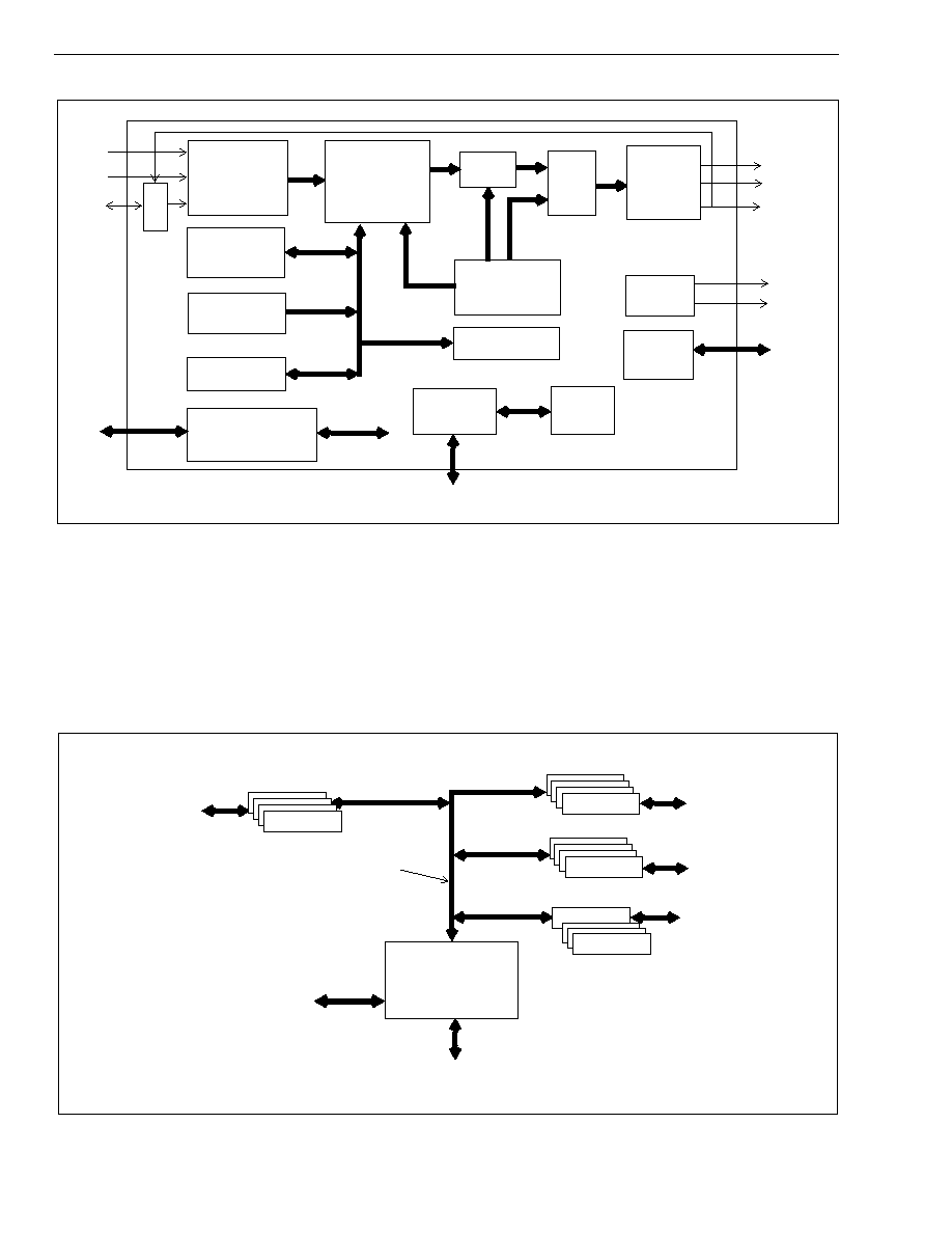
By integrating key functions needed in voice telecom
application, the Integrated Digital Switch (IDX)
provides a solution-on-a-chip for key telephone
systems, PBX applications or CTI designs. Figure 2
shows a typical configuration.
The MT90812 provides non-blocking timeslot
interchange capability for B, C and D channels, up to
a maximum of 192 channels. It offers conference call
capability for 15 parties over a maximum of 5
conference bridges. With its integrated PLL, the
MT90812 provides the necessary clocks to support
peripheral devices, such as codecs or
interconnected IDX devices. Integrated into the IDX
is the capability to detect supervisory signalling and
to generate FSK 1200-baud signals. In addition, an
integrated digital tone generator produces
continuous dual tones, including standard DTMF.
With its programmable gain control, the IDX allows
users to use codecs without gain control and also
centrally manage conference calls.
To support both small and large switching platforms,
a built-in expansion Bus allows the interconnection of
up to 4 IDX devices or external components such as
digital switches. When 4 IDX devices are
interconnected, the array is capable of switching 256
channels (64x4), handling 60 conference parties
(15x4) and generating additional tones including
programmable ones. Other functions are also
increased in this configuration. The functional block
diagram is shown in Figure 1.
An evaluation board, MEB90812, is available
complete with software and a user manual, which
demonstrates the layout of a typical application
board and facilitates the use of the MT90812, and
peripheral devices such as Zarlink's DNIC products.
DS5219
ISSUE 2
December 1999
Ordering Information
MT90812AP
68 Pin PLCC
MT90812AL
64 Pin MQFP
-40 to +85
∞
C
MT90812
Integrated Digital Switch (IDX)
Advance Information
MT90812
Advance Information
2
Figure 1 - Functional Block Diagram
Figure 2 - System Blocks - Typical Configuration
STi0
STi1
STo0
STo1
Serial
to
Parallel
Converter
Output
Mux
Parallel
to
Serial
Converter
Microprocessor
Connect Memory
Interface
EST1
M
U
X
EST0
FSK and Tone
Conference
D-channel
TX/RX
HDLC
Resource
Allocator
HDLC
Controller
PLL
Timing
&
Control
Frame Pulses and Clocks
CPU
Gain
Control
Energy Detect
Ring
R+
R-
Data
Memory
Frequency
Generation
Local
C.O.
Trunks
2B+D
Ports
Analog
Integrated
System Expansion bus (TDM)
MPU Interface
- D-channel
- Chip control
Ports
Digital Switch
- digital switch
- conferencing
- tone generation
- energy detection
2B+D
2B+D
2B+D
2B+D
2B+D
2B+D
2B+D
2B+D
TDM Bus
2B+D
Ports
CODEC
. ..
2B+D
2B+D
2B+D
CODEC
Advance Information
MT90812
3
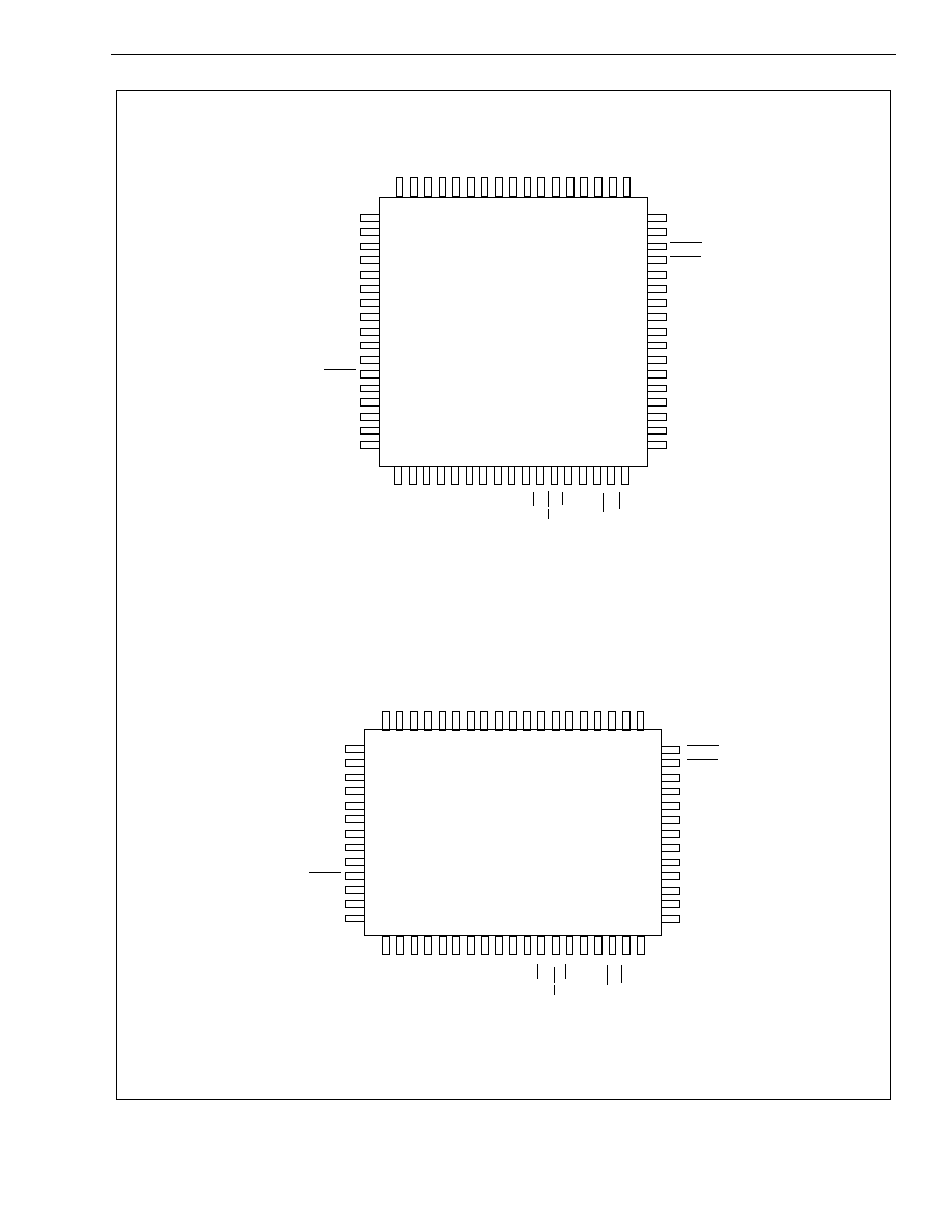
Figure 3 - Pin Connections
60
27
NC
IC
28 29 30 31 32 33 34 35 36 37 38 39 40 41 42 43
9
8
7
6
5
4
3
2 1 68 67 66 65 64 63 62 61
59
58
57
56
55
54
53
52
51
50
49
48
47
46
45
44
NC
RxCEN
TxCEN
REOP
TEOP
VSS1
AD7
AD6
AD5
AD4
AD3
AD2
AD1
AD0
VSS5
NC
VBUF
VSSA
VDDA
F4o
C2o
C4o
C10o
VSS3
R+
R -
RESET
IC
VDD
VSS4
NC
NC
NC
C4i
FPi
OSCo
C8P_C16i
F8
C8
ODE
EST1
EST0
DPER
STo1
STo0
STi1
STi0
VSS2
NC
A0
A1
A2
A3
A4
A5
A6
A7
A8
A9
DS/
RD
CS
AS/ALE
IRQ
10
11
12
13
14
15
16
17
18
19
20
21
22
23
24
25
26
68 PIN PLCC
IM
DTA
R/
W
\
WR
64 PIN MQFP
17
19
15
13
11
9
7
5
3
1
2
NC
NC
VSS2
STi0
STi1
STo0
STo1
DPER
EST0
EST1
ODE
C8
F8
C8P_C16i
OSCo
FPi
C4i
IC
REOP
VSS1
AD7
AD6
AD5
AD4
AD3
AD2
AD1
AD0
RxCEN
TEOP
TxCEN
VSS5
A2
A1
AS/ALE
CS
R/
W
\
WR
DS/
RD
A9
A8
A6
IRQ
DTA
A0
A3
A4
NC
A5
A7
VSSA
VDDA
F4o
C2o
C10o
RESET
VDD
C4o
VSS3
R+
R -
IC
VSS4
4
6
8
10
12
14
16
18
VBUF
32
31
30
29
28
27
26
25
24
23
22
21
20
52
53
54
55
56
57
58
59
60
60
62
63
64
IM
51
49 48
50
47 46 45 44 43 42 41 40 39 38 37 36 35 34 33
MT90812
Advance Information
4
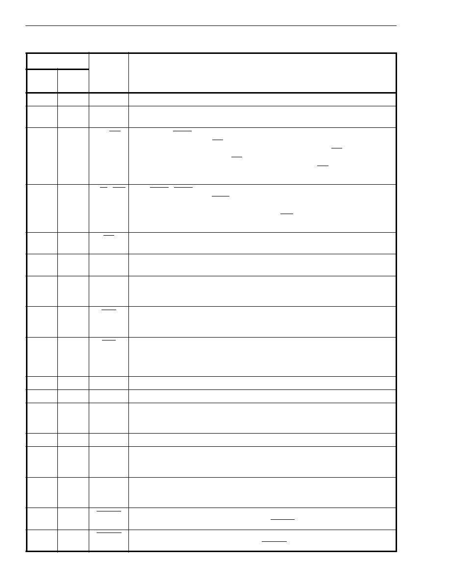
Pin Description
Pin #
Name
Description
64 Pin
MQFP
68 Pin
PLCC
1
25-26
NC
No Connect
. Ground
2-11
27-36
A0 - A9
Address 0 - 9(Input)
. When non-multiplexed CPU bus is selected, these lines
provide the A0 - A9 address lines to IDX internal memories.
12
37
DS/RD
Data Strobe/Read (Input)
. For Motorola multiplexed bus operation, this active
high DS input works with CS to enable the read and write operations.
For Motorola non-multiplexed CPU bus operation, this input is DS. This active low
input works in conjunction with CS to enable the read and write operations.
For Intel/National multiplexed bus operations, this input is RD. This active low
input sets the data bus lines (AD0-AD7) as outputs.
13
38
R/W \ WR
Read/Write \ Write (Input)
. In case of non-multiplexed and Motorola multiplexed
buses, this input is Read/Write. This input controls the direction of the data bus
lines (AD0 - AD7) during a microprocessor access.
For Intel/National multiplexed bus, this input is WR. This active low signal
configures the data bus lines (AD0-AD7) as inputs.
14
39
CS
Chip Select (Input)
. Active low input enabling a microprocessor read or write of
internal memories.
15
40
AS/ALE
Address Strobe or Latch Enable (Input)
. This input is only used if multiplexed
bus is selected via IM input pin.
16
41
IM
CPU Interface Mode (Input)
. If High, this input sets the device in the multiplexed
microprocessor mode. If this input is grounded, the device resumes non-
multiplexed CPU interface.
17
42
DTA
Data Acknowledgment (Open Drain Output)
.
This active low output indicates
that a data bus transfer is complete. A 10Kohm pull-up resistor is required at this
output.
18
43
IRQ
Interrupt Request Output (Open Drain Output)
. This active low output notifies
the controlling microprocessor of an interrupt request. It goes Low only when the
bits in the Interrupt Enable Register are programmed to acknowledge the source
of the interrupt as defined in the Interrupt Status Register.
-
44
NC
No Connect
. Ground
19
45
VSS5
Ground
.
20-27
46-53
AD0 - AD7
Data Bus (Bidirectional)
. These pins provide microprocessor access to the
internal memories. In the multiplexed bus mode, these pins also provide the input
address to the internal Address Latch circuit.
28
54
VSS1
Ground
.
29
55
TEOP
Transmit End of Packet (Input)
. This is a strobe that is generated by the HDLC
controller chip for one bit period during the last bit of the closing flag of the
transmit packet.
30
56
REOP
Receive End of Packet (Input)
. A receive packet will normally be terminated
when the HDLC controller asserts the REOP strobe for one bit period, one bit time
after the closing flag is received.
31
57
TxCEN
Transmit Clock Enable (Output)
. The HDLC transmitter is controlled by the IDX-
generated Transmit Clock Enable signal, TxCEN.
32
58
RxCEN
Receive Clock Enable (Output)
. The HDLC receiver is controlled by the IDX-
generated Receive Clock Enable signal, RxCEN.

Advance Information
MT90812
5
33-34
59-61
NC
No Connect
. Ground
35
62
VSS2
Ground
.
36-37
63-64
STi0-1
Serial TDM input streams 0 and 1 (Input)
. Serial data input streams which have
data rates of 2.048 Mb/s with 32 channels.
38-39
65-66
STo0-1
Serial TDM output streams 0 and 1 (Three-state output)
. Serial data output
streams which have data rates of 2.048 Mb/s with 32 channels.
40
67
DPER
D-Channel Input in ST-BUS format (Input)
. The MT8952B CDSTo stream
containing formatted D-channel data.
41
68
EST0
Expansion Bus Serial data stream 0 (Three-state output/input)
. This is a bi-
directional pin at 8.192 Mb/s in IDX Link mode. In TDM Link mode this is a 2.048,
4.096 or 8.192 Mb/s output stream.
42
1
EST1
Expansion Bus Serial data stream 1 (Three-state output/input)
. This is a bi-
directional pin at 8.192 Mb/s in IDX Link mode. In TDM Link mode this is a 2.048,
4.096 or 8.192 Mb/s input stream.
43
2
ODE
Output Device Enable (Input)
. This is the output enable input for the serial
outputs. If this input is low, STo0, STo1, EST0, EST1 are high impedance. If this
input is high, each channel may still be put into high impedance state by using per
channel control bit in the Connection Memory.
44
3
C8
Clock 8.192 (Bidirectional)
. As an input this signal is used for Expansion bus
and/or internal clock source at 8.192 MHz depending on the timing mode
selected. As an output this signal is an 8.192 MHz output clock locked to the
reference input signal.
45
4
F8
Frame Pulse for 8.192 MHz (Bidirectional)
. As an input accepts and
automatically identifies frame synchronization signals formatted according to ST-
BUS and GCI interface specifications. As an output is an 8 KHz frame pulse that
indicates the start of the active frame. Either F8 or FPi are used for frame
synchronization depending on the timing mode selected
46
5
C8P_C16i
Oscillator Master Clock (CMOS Input)
. For crystal operation, a 8.192MHz
crystal is connected to this pin from OSCo. For clock oscillator operation, this pin
is connected to a clock source. The clock source of either 8.192 MHz or 16.384
MHz can be used as selected in the Timing Control Register (TC).
47
6
OSCo
Oscillator Master Clock (CMOS Output)
. For crystal operation, a 8.192MHz
crystal is connected from this pin to C8P_C16i. For clock oscillator operation, this
pin is left unconnected.
48
7
FPi
Frame Pulse (Input).
This input accepts and automatically identifies frame
synchronization signals formatted according to ST-BUS and GCI interface
specifications. Either F8 or FPi are used for frame synchronization depending on
the timing mode selected.
49
8
C4i
Clock 4.096 MHz (Input)
. This input is the 4.096 MHz clock input.
-
9
NC
No Connect
. Ground
50-51
10-11
IC
Internal Connect
. Open.
52
12
VSSA
Analog Ground
.
53
13
VDDA
+5 Volt Power Supply (Analog)
.
Pin Description (continued)
Pin #
Name
Description
64 Pin
MQFP
68 Pin
PLCC