Document Outline
- Features
- Applications
- Description
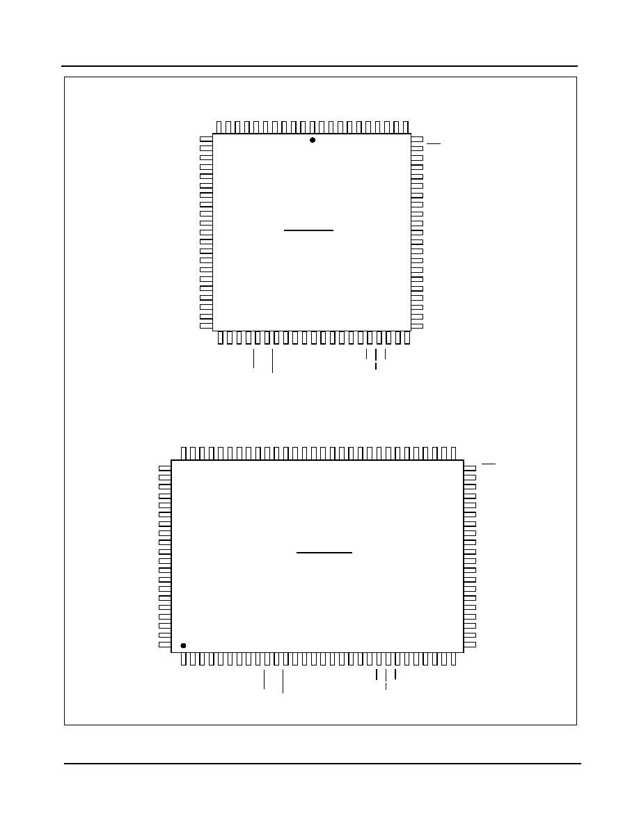
- Figure 2 - PLCC and MQFP Pin Connections
- Figure 3 - PBGA and LQFP Pin Connections
- Pin Description�
- Device Overview
- Functional Description
- Data and Connection Memory
- Connection and Message Modes
- Serial Data Interface Timing
- Wide Frame Pulse (WFP) Frame Alignment Timing
- Switching Configurations
- Table 1 - Switching Configuration
- Input Frame Offset Selection
- Serial Input Frame Alignment Evaluation
- Memory Block Programming
- Loopback Control
- Delay Through the MT90823
- Variable Delay Mode (V/C bit = 0)
- Constant Delay Mode (V/C bit = 1)
- Microprocessor Interface
- Table 2 - Variable Throughput Delay Value
- Table 3 - Constant Throughput Delay Value
- Memory Mapping
- Connection Memory Control
- Table 4 - Internal Register and Address Memory Mapping
- Table 5 - Output High Impedance Control
- Initialization of the MT90823
- Table 6 - Control (CR) Register Bits
- Table 7 - Valid Address lines for Different Bit Rates
- Table 8 - Interface Mode Selection (IMS) Register Bits
- Table 9 - Serial Data Rate Selection (16 input x 16 output)
- Table 10 - Frame Alignment (FAR) Register Bits
- Figure 4 - Example for Frame Alignment Measurement
- Table 11 - Frame Input Offset (FOR) Register Bits
- Table 12 - Offset Bits (OFn2, OFn1, OFn0, DLEn) and Frame Delay Bits (FD11, FD2-0)
- Figure 5 - Examples for Input Offset Delay Timing
- Table 13 - Connection Memory Bits
- JTAG Support
- Test Access Port (TAP)
- Instruction Register
- Test Data Register
- Table 14 - Boundary Scan Register Bits�
- Applications
- Switch Matrix Architectures
- Serial Input Frame Alignment Evaluation
- Figure 6 - Switch Matrix with Serial Stream at Various Bit Rates
- Figure 7 - Serial Input Frame Alignment Evaluation for Various Frame Pulses
- Wide Frame Pulse (WFP) Frame Alignment Mode
- Digital Access Cross-Connect System
- Figure 8 - 256 E1/T1 Digital Access Cross-Connect System (DACS)
- Figure 9 - 8,192 x 8,192 Channel Switch Matrix
- Figure 10 - Trunk Card Block Diagram
- Absolute Maximum Ratings*
- Recommended Operating Conditions - Voltages are with respect to ground (Vss) unless otherwise sta...
- DC Electrical Characteristics - Voltages are with respect to ground (Vss) unless otherwise stated.
- AC Electrical Characteristics - Timing Parameter Measurement Voltage Levels
- AC Electrical Characteristics - Frame Pulse and CLK
- AC Electrical Characteristics - Serial Streams for ST-BUS and GCI Backplanes
- Figure 11 - ST-BUS Timing for 2.048 Mb/s and High Speed Serial Interface at 4.096 Mb/s or 8.192 M...
- Figure 12 - GCI Timing at 2.048 Mb/s and High Speed Serial Interface at 4.096 Mb/s or 8.192 Mb/s,...
- Figure 13 - WFP Bus Timing for High Speed Serial Interface (8.192�Mb/s), when WFPS pin = 1
- Figure 14 - Serial Output and External Control
- Figure 15 - Output Driver Enable (ODE)
- AC Electrical Characteristics - Multiplexed Bus Timing (Mode 1)
- Figure 16 - Multiplexed Bus Timing (Mode 1)
- AC Electrical Characteristics - Multiplexed Bus Timing (Mode 2)
- Figure 17 - Multiplexed Bus Timing (Mode2)
- AC Electrical Characteristics - Motorola Non-Multiplexed Bus Mode
- Figure 18 - Motorola Non-Multiplexed Bus Timing
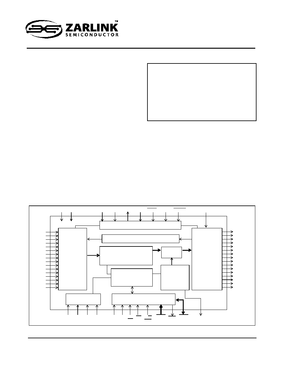
- Figure 1 - Functional Block Diagram
1
Zarlink Semiconductor Inc.
Zarlink, ZL and the Zarlink Semiconductor logo are trademarks of Zarlink Semiconductor Inc.
Copyright 2003-2005, Zarlink Semiconductor Inc. All Rights Reserved.
Features
� 2,048
� 2,048 channel non-blocking switching at
8.192 Mb/s
� Per-channel variable or constant throughput
delay
� Automatic identification of ST-BUS/GCI interfaces
� Accept ST-BUS streams of 2.048, 4.096 or
8.192 Mb/s
� Automatic frame offset delay measurement
� Per-stream frame delay offset programming
� Per-channel high impedance output control
� Per-channel message mode
� Control interface compatible to Motorola non-
multiplexed CPUs
� Connection memory block programming
� 3.3 V local I/O with 5 V tolerant inputs and TTL-
compatible outputs
� IEEE-1149.1 (JTAG) Test Port
Applications
� Medium and large switching platforms
� CTI application
� Voice/data multiplexer
� Digital cross connects
� ST-BUS/GCI interface functions
� Support IEEE 802.9a standard
July 2005
Ordering Information
MT90823AP
84 Pin PLCC
Tubes
MT90823AL
100 Pin MQFP
Trays
MT90823AB
100 Pin LQFP
Trays
MT90823AG
120 Pin BGA
Trays
MT90823AB1
100 Pin LQFP*
Trays
MT90823AP1
84 Pin PLCC*
Tubes
MT90823AL1
100 Pin MQFP*
Trays
*Pb Free Matte Tin
-40
�C to +85�C
MT90823
3 V Large Digital Switch
Data Sheet
Figure 1 - Functional Block Diagram
Test Port
STo0
STo1
STo2
STo3
STo4
STo5
STo6
STo7
STo8
STo9
STo10
STo11
STo12
STo13
STo14
STo15
STi0
STi1
STi2
STi3
STi4
STi5
STi6
STi7
STi8
STi9
STi10
STi11
STi12
STi13
STi14
STi15
Parallel
to
Serial
Converter
Output
MUX
Microprocessor Interface
Timing
Unit
Internal
Registers
F0i
FE/
AS/ IM DS/
RD
CS R/W
/WR
A7-A0
ALE
HCLK
DTA D15-D8/
AD7-AD0
CSTo
ODE
V
SS
Connection
Memory
CLK
V
DD
WFPS
TDI
TDO
IC
RESET
TCK TRST
Serial
to
Parallel
Converter
TMS
Multiple Buffer
Data Memory
Loopback

MT90823
Data Sheet
2
Zarlink Semiconductor Inc.
Description
The MT90823 Large Digital Switch has a non-blocking switch capacity of: 2,048 x 2,048 channels at a serial bit rate
of 8.192 Mb/s; 1,024 x 1,024 channels at 4.096 Mb/s; and 512 x 512 channels at 2.048 Mb/s. The device has many
features that are programmable on a per stream or per channel basis, including message mode, input offset delay
and high impedance output control.
Per stream input delay control is particularly useful for managing large multi-chip switches that transport both voice
channel and concatenated data channels.
In addition, the input stream can be individually calibrated for input frame offset using a dedicated pin.
MT90823
Data Sheet
3
Zarlink Semiconductor Inc.
Figure 2 - PLCC and MQFP Pin Connections
NC
NC
NC
NC
NC
73
57
59
61
63
65
69
71
67
13
29
27
25
23
19
17
15
21
31
55
10
8
6
4
2
84
82
80
78
76
34
36
38
40
42
44
46
48
50
52
D14
D12
D11
D10
D9
D8
AD2
AD1
AD0
VSS
VSS
VDD
AD7
AD6
AD5
AD4
AD3
DTA
D13
D15
CSTo
AS/AL
E
TC
K
TD
O
A7
A6
A5
A4
A3
A2
A1
A0
CS
DS/
R
D
IM
TD
I
TR
S
T
IC
RESE
T
WFPS
TMS
R/
W
/R
W
STi0
STi1
STi2
STi3
STi4
STi5
STi6
STi7
STi8
STi9
STi11
STi15
FE/HCLK
STi10
STi12
STi13
STi14
F0i
VDD
CLK
VSS
ODE
ST
o
0
ST
o
1
ST
o
2
ST
o
3
ST
o
4
ST
o
5
ST
o
6
ST
o
7
VS
S
VD
D
VS
S
ST
o
8
ST
o
9
ST
o
1
0
ST
o
1
1
ST
o
1
2
ST
o
1
3
ST
o
1
4
ST
o
1
5
VS
S
84 PIN PLCC
100 PIN MQFP
50
52
54
56
58
60
62
64
66
68
70
72
74
76
78
80
22
24
26
28
30
32
34
36
38
40
44
46
48
42
82
98
96
94
92
88
86
84
90
20
18
16
14
12
10
8
6
4
2
OD
E
ST
o0
ST
o1
ST
o2
ST
o3
ST
o4
ST
o5
ST
o6
ST
o7
VSS
VDD
VSS
ST
o8
ST
o9
ST
o1
0
ST
o1
1
ST
o1
2
ST
o1
3
ST
o1
4
ST
o1
5
VSS
CS
T
o
NC
NC
NC
NC
D14
D12
D11
D10
D9
D8
AD2
AD1
AD0
VSS
VSS
VDD
AD7
AD6
AD5
AD4
AD3
DTA
D13
D15
CS
TC
K
TD
O
A7
A6
A5
A4
A3
A2
A1
WF
PS
R/
W
/R
W
DS
/
R
D
TDI
TRST
IC
TMS
AS/ALE
VD
D
RE
SET
A0
IM
NC
NC
NC
NC
NC
STi0
STi1
STi2
STi3
STi4
STi5
STi6
STi7
STi8
STi9
STi11
STi15
FE/HCLK
STi10
STi12
STi13
STi14
F0i
CLK
VSS
NC
NC
99
(14mm x 20mm x 2.75mm)

MT90823
Data Sheet
4
Zarlink Semiconductor Inc.
Figure 3 - PBGA and LQFP Pin Connections
D14
D12
D11
D10
D9
D8
AD2
AD1
AD0
VSS
VSS
VDD
AD7
AD6
AD5
AD4
AD3
DTA
D13
D15
CSTo
AS/ALE
TCK
TDO
A7
A6
A5
A3
A4
A2
A1
A0
CS
DS/RD
IM
TDI
TRST
IC
RESET
WFPS
TMS
R/W/RW
STi0 STi1
STi2 STi3
STi4 STi5
STi6 STi7
STi8 STi9
STi11
STi15
FE/HCLK
STi10
STi12 STi13
STi14
F0i
VDD
CLK
VSS
ODE
STo0
STo1
STo2
STo3
STo4
STo5
STo6
STo7
VSS
VDD
VSS
STo8
STo9
STo10
STo11
STo12
STo13
STo14
STo15
VSS
VSS
VDD
VSS
VDD
VSS
VDD
VSS
VDD
VSS
VSS
VSS
VDD
VSS
VSS VSS
VSS
VSS
VDD
VSS
VSS
VSS
VSS
VSS
VSS
VDD
VDD
VDD
VSS
VSS
VSS
VDD
VDD
VDD
VDD VSS
VSS
A
B
C
D
E
F
G
H
J
K
L
M
N
1
2
3
4
5
6
7
8
9
10
11
12
13
TOP VIEW
1
1 - A1 corner is identified by metallized markings.
PBGA
NC
NC
CSTo
NC
100 PIN LQFP
52
76
2
OD
E
ST
o0
ST
o1
ST
o2
ST
o3
ST
o4
ST
o5
ST
o6
ST
o7
VS
S
VD
D
VS
S
ST
o8
ST
o9
ST
o10
ST
o1
1
ST
o12
ST
o13
ST
o14
ST
o15
VS
S
NC
NC
NC
D14
D12
D11
D10
D9
D8
AD2
AD1
AD0
VSS
VSS
VDD
AD7
AD6
AD5
AD4
AD3
DTA
D13
D15
CS
TCK
TDO
A7
A6
A5
A4
A3
A2
A1
WF
P
S
R/
W
/R
W
DS
/RD
TD
I
TR
ST
IC
TMS
AS
/ALE
RE
SE
T
A0
IM
NC
NC
STi0
STi1
STi2
STi3
STi4
STi5
STi6
STi7
STi8
STi9
STi11
STi15
FE/HCLK
STi10
STi12
STi13
STi14
F0i
CLK
VSS
NC
100
NC
NC
NC
NC
NC
VDD
26
50
NC
NC
(Ball Pitch = 1.5mm)
(23mm x 23mm x 2.13mm)
(14mm x 14mm x 1.4mm)
(Pin Pitch = 0.50mm)
4
6
8
10
12
14
16
18
20
22
24
28
30
32
34
36
38
40
42
44
46
48
54
56
58
60
62
64
66
68
70
72
74
78
80
82
84
86
88
90
92
94
96
98

MT90823
Data Sheet
5
Zarlink Semiconductor Inc.
Pin Description
Pin #
Name
Description
84
PLCC
100
MQFP
100
LQFP
120
BGA
1, 11,
30, 54
64, 75
31, 41,
56, 66,
76, 99
28,
38,
53,
63,
73,
96
A1,A2,A12,A13,
B1,B2,B7,B12,
B13,C3,C5,C7,
C9,C11,E3,E11
G3,G11,J3,J11,
L3,L5,L7,L9,L11,
M1,M2,M12,M13
V
SS
Ground.
2, 32,
63
5, 40,
67
37,
64,98
C4,C6,C8,C10,
D3,D11,F3,F11,
H3,H11,K3,K11,
L4,L6,L8,L10
V
DD
+3.3 Volt Power Supply.
3 - 10
68-75
65 -
72
B6,A6,A5,B5,A4,
B4,A3,B3
STo8 - 15 ST-BUS Output 8 to 15 (5 V Tolerant Three-state
Outputs): Serial data Output stream. These streams
may have data rates of 2.048, 4.096 or 8.192 Mb/s,
depending upon the value programmed at bits DR0 - 1
in the IMS register.
12 -
27
81-96
78 -
93
C1,C2,D1,D2,E1,
E2,F1,F2,G1,G2,
H1,H2,J1,J2,K1,
K2
STi0 - 15 ST-BUS Input 0 to 15 (5 V Tolerant Inputs): Serial
data input stream. These streams may have data rates
of 2.048, 4.096 or 8.192 Mb/s, depending upon the
value programmed at bits DR0 - 1 in the IMS register.
28
97
94
L1
F0i
Frame Pulse (5 V Tolerant Input): When the WFPS
pin is low, this input accepts and automatically
identifies frame synchronization signals formatted
according to ST-BUS and GCI specifications. When the
WFPS pin is high, this pin accepts a negative frame
pulse which conforms to WFPS formats.
29
98
95
L2
FE/HCLK Frame Evaluation / HCLK Clock (5 V Tolerant
Input): When the WFPS pin is low, this pin is the frame
measurement input. When the WFPS pin is high, the
HCLK (4.096MHz clock) is required for frame
alignment in the wide frame pulse (WFP) mode.
31
100
97
N1
CLK
Clock (5 V Tolerant Input): Serial clock for shifting
data in/out on the serial streams (STi/o 0 - 15).
Depending upon the value programmed at bits DR0 - 1
in the IMS register, this input accepts a 4.096, 8.192 or
16.384 MHz clock.
33
6
3
N2
TMS
Test Mode Select (3.3 V Input with internal pull-up):
JTAG signal that controls the TAP controller state
transitions.
34
7
4
M3
TDI
Test Serial Data In (3.3 V Tolerant Input with internal
pull-up): JTAG serial test instructions and data are
shifted in on this pin.