 | –≠–ª–µ–∫—Ç—Ä–æ–Ω–Ω—ã–π –∫–æ–º–ø–æ–Ω–µ–Ω—Ç: MT9172AE | –°–∫–∞—á–∞—Ç—å:  PDF PDF  ZIP ZIP |
9-115
9-115
Features
∑
Full duplex transmission over a single twisted
pair
∑
Selectable 80 or 160 kbit/s line rate
∑
Adaptive echo cancellation
∑
Up to 3km (9171) and 4 km (9172)
∑
ISDN compatible (2B+D) data format
∑
Transparent modem capability
∑
Frame synchronization and clock extraction
∑
Zarlink ST-BUS compatible
∑
Low power (typically 50 mW), single 5V supply
Applications
∑
Digital subscriber lines
∑
High speed data transmission over twisted
wires
∑
Digital PABX line cards and telephone sets
∑
80 or 160 kbit/s single chip modem
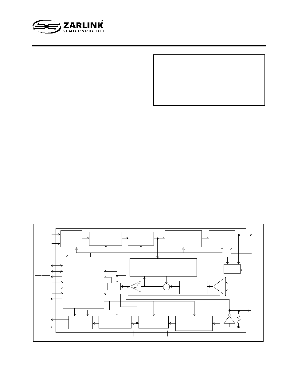
Figure 1 - Functional Block Diagram
DSTi/Di
CDSTi/
F0/CLD
C4/TCK
F0o/RCK
MS0
MS1
MS2
RegC
DSTo/Do
CDSTo/
CDo
Transmit
Interface
Prescrambler
Scrambler
Control
Register
Transmit/
Clock
Receive
Timing &
Control
Status
Transmit
Timing
Master Clock
Phase Locked
Sync Detect
Receive
DPLL
Receive
Interface
De-
Prescrambler
Descrambler
Differentially
Encoded Biphase
Receiver
Differentially
Encoded Biphase
Transmitter
Transmit
Filter &
Line Driver
Receive
Filter
-1
+2
MUX
Address
Echo Canceller
Error
Signal
Echo Estimate
V
Bias
V
DD
V
SS
V
Bias
V
Ref
L
OUT
L
OUT
DIS
Precan
L
IN
OSC2
OSC1
--
+
CDi
DS5130
ISSUE 3
February 1999
Description
The
MT9171 (DSIC) and MT9172 (DNIC) are pin for
pin compatible replacements for the MT8971 and
MT8972, respectively. They are multi-function
devices capable of providing high speed,
full duplex
digital transmission up to 160 kbit/s over a twisted
wire pair. They use adaptive echo-cancelling
techniques and transfer data in (2B+D) format
compatible to the ISDN basic rate. Several modes of
operation allow an easy interface to digital
telecommunication networks including use as a high
speed limited distance modem with data rates up to
160 kbit/s. Both devices function identically but with
the DSIC having a shorter maximum loop reach
specification. The generic "DNIC" will be used to
reference both devices unless otherwise noted.
The MT9171/72 is fabricated in Zarlink's ISO
2
-
CMOS process.
Ordering Information
MT9171AE
22 Pin Plastic DIP (400 mil)
MT9171AN
24 Pin SSOP
MT9171AP
28 Pin PLCC
MT9172AE
22 Pin Plastic DIP (400 mil)
MT9172AN
24 Pin SSOP
MT9172AP
28 Pin PLCC
-40
∞
C to
+
85
∞
C
MT9171/72
Digital Subscriber Interface Circuit
Digital Network Interface Circuit
ISO
2
-CMOS ST-BUS
FAMILY
MT9171/72
Advance Information
9-116
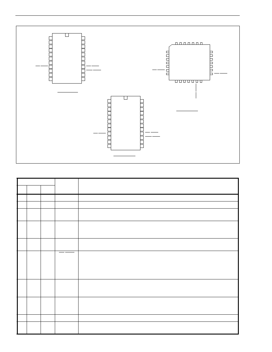
Figure 2 - Pin Connections
Pin Description
Pin #
Name
Description
22
24
28
1
1
2
L
OUT
Line Out.
Transmit Signal
output (Analog). Referenced to V
Bias
.
2
2
3
V
Bias
Internal Bias Voltage
output. Connect via 0.33
µ
F decoupling capacitor to V
DD
.
3
3
4
V
Ref
Internal Reference Voltage
output. Connect via 0.33
µ
F decoupling capacitor to
V
DD
.
4,5,
6
4,5,
6
5,7,
8
MS2-MS0
Mode Select
inputs (Digital). The logic levels present on these pins select the
various operating modes for a particular application. See Table 1 for the
operating modes.
7
7
9
RegC
Regulator Control
output (Digital). A 512 kHz clock used for switch mode power
supplies. Unused in MAS/MOD mode and should be left open circuit.
8
9
10
F0/CLD
Frame Pulse/C-Channel Load
(Digital). In DN mode a 244 ns wide negative
pulse input for the MASTER indicating the start of the active channel times of the
device. Output for the SLAVE indicating the start of the active channel times of
the device. Output in MOD mode providing a pulse indicating the start of the C-
channel.
9
10
12
CDSTi/
CDi
Control/Data ST-BUS In/Control/Data In
(Digital). A 2.048 Mbit/s serial control
& signalling input in DN mode. In MOD mode this is a continuous bit stream at
the bit rate selected.
10
11
13
CDSTo/
CDo
Control/Data ST-BUS Out/Control/Data Out
(Digital). A 2.048 Mbit/s serial
control & signalling output in DN mode. In MOD mode this is a continuous bit
stream at the bit rate selected.
11
12
14
V
SS
Negative Power Supply
(0V).
12
13
15
DSTo/Do
Data ST-BUS Out/Data Out
(Digital). A 2.048 Mbit/s serial PCM/data output in
DN mode. In MOD mode this is a continuous bit stream at the bit rate selected.
1
2
3
4
5
6
7
8
9
10
11
12
13
14
22
21
20
19
18
17
16
15
22 PIN PDIP
LOUT
VBias
VRef
MS2
MS1
MS0
RegC
F0/CLD
CDSTi/CDi
CDSTo/CDo
VSS
VDD
LIN
TEST
LOUT DIS
Precan
OSC1
OSC2
C4/TCK
F0o/RCK
DSTi/Di
DSTo/Do
28 PIN PLCC
27
4
3
2
1
28
26
5
6
7
8
9
10
11
25
24
23
22
21
20
19
17
12
13
14
15
16
18
∑
LOUT
VBias
VRef
NC
VDD
LIN
TEST
NC
LOUT DIS
Precan
OSC1
OSC2
NC
C4/TCK
MS2
NC
MS1
MS0
RegC
F0/CLD
NC
CDSTi/CDi
CDSTo/CDo
VSS
DSTo/Do
NC
F
0
o
/R
C
K
DSTi/Di
1
2
3
4
5
6
7
8
9
10
11
12
13
14
15
16
24
23
22
21
20
19
18
17
24 PIN SSOP
LOUT
VBias
VRef
MS2
MS1
MS0
RegC
F0/CLD
CDSTi/CDi
CDSTo/CDo
VSS
NC
VDD
LIN
TEST
LOUT DIS
Precan
OSC1
OSC2
C4/TCK
F0o/RCK
DSTi/Di
DSTo/Do
NC
Advance Information
MT9171/72
9-117
13
14
16
DSTi/Di
Data ST-BUS In/Data In
(Digital). A 2.048 Mbit/s serial PCM/data input in DN
mode. In MOD mode this is a continuous bit stream at the bit rate selected.
14
15
17
F0o/RCK
Frame Pulse Out/Receive Bit Rate Clock
output (Digital). In DN mode a 244 ns
wide negative pulse indicating the end of the active channel times of the device to
allow daisy chaining. In MOD mode provides the receive bit rate clock to the
system.
15
16
19
C4/TCK
Data Clock/Transmit Baud Rate Clock
(Digital). A 4.096 MHz TTL compatible
clock input for the MASTER and output for the SLAVE in DN mode. For MOD
mode this pin provides the transmit bit rate clock to the system.
16
17
21
OSC2
Oscillator Output
. CMOS Output.
17
19
22
OSC1
Oscillator Input
. CMOS Input. D.C. couple signals to this pin. Refer to D.C.
Electrical Characteristics for OSC1 input requirements.
18
20
23
Precan
Precanceller Disable.
When held to Logic '1
',
the internal path from L
OUT
to the
precanceller is forced to V
Bias
thus bypassing the precanceller section. When
logic '0', the L
OUT
to the precanceller path is enabled and functions normally. An
internal pulldown (50 k
) is provided on this pin.
8,
18
1,6,
11,
18,
20,
25
NC
No Connection.
Leave open circuit
19
21
24
L
OUT
DIS
L
OUT
Disable.
When held to logic "1", L
OUT
is disabled (i.e., output = V
Bias
). When
logic "0", L
OUT
functions normally. An internal pulldown (50 k
) is provided on this
pin.
20
22
26
TEST
Test Pin.
Connect to V
SS
.
21
23
27
L
IN
Receive Signal
input (Analog).
22
24
28
V
DD
Positive Power Supply
(+5V) input.
Pin Description (continued)
Pin #
Name
Description
22
24
28
MT9171/72
Advance Information
9-118
Figure 3 - DV Port - 80 kbit/s (Modes 2, 3, 6)
Figure 4 - DV Port - 160 kbit/s (Modes 2, 3, 6)
F0
C4
DSTi
DSTo
F0o
B1
7
B1
6
B1
5
B1
4
B1
3
B1
2
B1
1
B1
0
B1
7
B1
6
B1
5
B1
4
B1
3
B1
2
B1
1
B1
0
B1
7
B1
7
Channel Time 0
F0
C4
DSTi
DSTo
F0o
B1
7
B1
6
B1
5
B1
4
B1
3
B1
2
B1
1
B1
0
B1
7
B1
7
Channel Time 0
B1
7
B1
6
B1
5
B1
4
B1
3
B1
2
B1
1
B1
0
B2
7
B2
6
B2
5
B2
4
B2
3
B2
2
B2
1
B2
0
B2
7
B2
6
B2
5
B2
4
B2
3
B2
2
B2
1
B2
0
Channel Time 16

Advance Information
MT9171/72
9-119
Functional Description
The MT9171/72 is a device which may be used in
practically any application that requires high speed
data transmission over two wires, including smart
telephone sets, workstations, data terminals and
computers. The device supports the 2B+D channel
format (two 64 kbit/s B-channels and one 16 kbit/s D-
channel) over two wires as recommended by the
CCITT. The line data is converted to and from the ST-
BUS format on the system side of the network to
allow for easy interfacing with other components
such as the S-interface device in an NT1
arrangement, or to digital PABX components.
Smart telephone sets with data and voice capability
can be easily implemented using the MT9171/72 as
a line interface. The device's high bandwidth and
long loop length capability allows its use in a wide
variety of sets. This can be extended to provide full
data and voice capability to the private subscriber by
the installation of equipment in both the home and
central office or remote concentration equipment.
Within the subscriber equipment the MT9171/72
would terminate the line and encode/ decode the
data and voice for transmission while additional
electronics could provide interfaces for a standard
telephone set and any number of data ports
supporting standard data rates for such things as
computer communications and telemetry for remote
meter reading. Digital workstations with a high
degree of networking capability can be designed
using the DNIC for the line interface, offering up to
160 kbit/s data transmission over existing telephone
lines. The MT9171/72 could also be valuable within
existing computer networks for connecting a large
number of terminals to a computer or for
intercomputer links. With the DNIC, this can be
accomplished at up to 160 kbit/s at a very low cost
per line for terminal to computer links and in many
cases this bandwidth would be sufficient for
computer to computer links.
Figure 1 shows the block diagram of the MT9171/72.
The DNIC provides a bidirectional interface between
the DV (data/voice) port and a full duplex line
operating at 80 or 160 kbit/s over a single pair of
twisted wires. The DNIC has three serial ports. The
DV port (DSTi/Di, DSTo/Do), the CD (control/data)
port (CDSTi/CDi, CDSTo/CDo) and a line port (L
IN
,
L
OUT
). The data on the line is made up of information
from the DV and CD ports. The DNIC must combine
information received from both the DV and CD ports
and put it onto the line. At the same time, the data
received from the line must be split into the various
channels and directed to the proper ports. The
usable data rates are 72 and
144 kbit/s as required
for the basic rate interface in ISDN. Full duplex
transmission is made possible through on board
adaptive echo cancellation.
The DNIC has various modes of operation which are
selected through the mode select pins MS0-2. The
two major modes of operation are the MODEM
(MOD) and DIGITAL NETWORK (DN) modes. MOD
mode is a transparent 80 or 160 kbit/s modem. In
DN mode the line carries the B and D channels
formatted for the ISDN at either 80 or 160 kbit/s. In
the DN mode the DV and CD ports are standard ST-
BUS and in MOD mode they are transparent serial
data streams at 80 or 160 kbit/s. Other modes
include: MASTER (MAS) or SLAVE (SLV) mode,
where the timebase and frame synchronization are
provided externally or are extracted from the line and
DUAL or SINGLE (SINGL) port modes, where both
the DV and CD ports are active or where the CD port
is inactive and all information is passed through the
DV port. For a detailed description of the modes
see
"Operating Modes" section.
In DIGITAL NETWORK (DN) mode there are three
channels transferred by the DV and CD ports. They
are the B, C and D channels. The B1 and B2
channels each have a bandwidth of 64 kbit/s and are
used for carrying PCM encoded voice or data. These
channels are always transmitted and received
through the DV port (Figures 3, 4, 5, 6). The C-
channel, having a bandwidth of 64 kbit/s, provides a
means for the system to control the DNIC and for the
DNIC to pass status information back to the system.
The C-channel has a Housekeeping (HK) bit which is
the only bit of the C-channel transmitted and
received on the line. The 2B+D channel bits and the
HK bit are double-buffered. The D-channel can be
transmitted or received on the line with either an 8,
16 or 64 kbit/s bandwidth depending on the DNIC's
mode of operation. Both the HK bit and the D-
channel can be used for end-to-end signalling or low
speed data transfer. In DUAL port mode the C and D
channels are accessed via the CD port (Figure 7)
while in SINGL port mode they are transferred
through the DV port (Figures 5, 6) along with the B1
and B2 channels.