 | –≠–ª–µ–∫—Ç—Ä–æ–Ω–Ω—ã–π –∫–æ–º–ø–æ–Ω–µ–Ω—Ç: MT93L04A | –°–∫–∞—á–∞—Ç—å:  PDF PDF  ZIP ZIP |

1
Features
∑
MT93L04
is a Multi-chip Module (MCM)
consisting of 4 MT93L00 devices thus providing
128 channels of 64 msec Echo Cancellation.
∑
Each device (MT93L00) is independent of the
each other.
∑
Each device has the capability of cancelling
echo over 32 channels.
∑
The MCM module provides more than 40%
board space savings.
∑
Each device (MT93L00) can be programmed
independently in any mode e.g back to back or
extended delay to provide capability of
cancelling different echo tails.
∑
Each device has the same Jtag identification
code.
Applications
∑
Voice over IP network gateways
∑
Voice over ATM, Frame Relay
∑
T1/E1/J1 multichannel echo cancellation
∑
Wireless base stations
∑
Echo Canceller pools
∑
DCME, satellite and multiplexer systems
Description
The MT93L04 Voice Echo Canceller implements a
cost effective solution for telephony voice-band echo
cancellation conforming to ITU-T G.168
requirements. The MT93L04 architecture contains
64 groups of two echo cancellers (ECA and ECB)
which can be configured to provide two channels of
64 milliseconds or one channel of 128 milliseconds
echo cancellation. This provides 128 channels of 64
milliseconds to 64 channels of 128 milliseconds echo
cancellation or any combination of the two
configurations. The MT93L04 supports ITU-T G.165
and G.164 tone disable requirements.
MT93L04 is MULTI-CHIP module consiting of 4 MT93L00 devices
1
3
2
MT93L00
MT93L00
MT93L00
MT93L00
4
Ordering Information
MT93L04AG 365 Ball BGA
40
∞
∞
C to +85
∞
∞
C
DS5524
ISSUE 2
September 2001
MT93L04A
128-Channel Voice Echo Canceller
Preliminary Information
MT93L04A
Preliminary Information
2
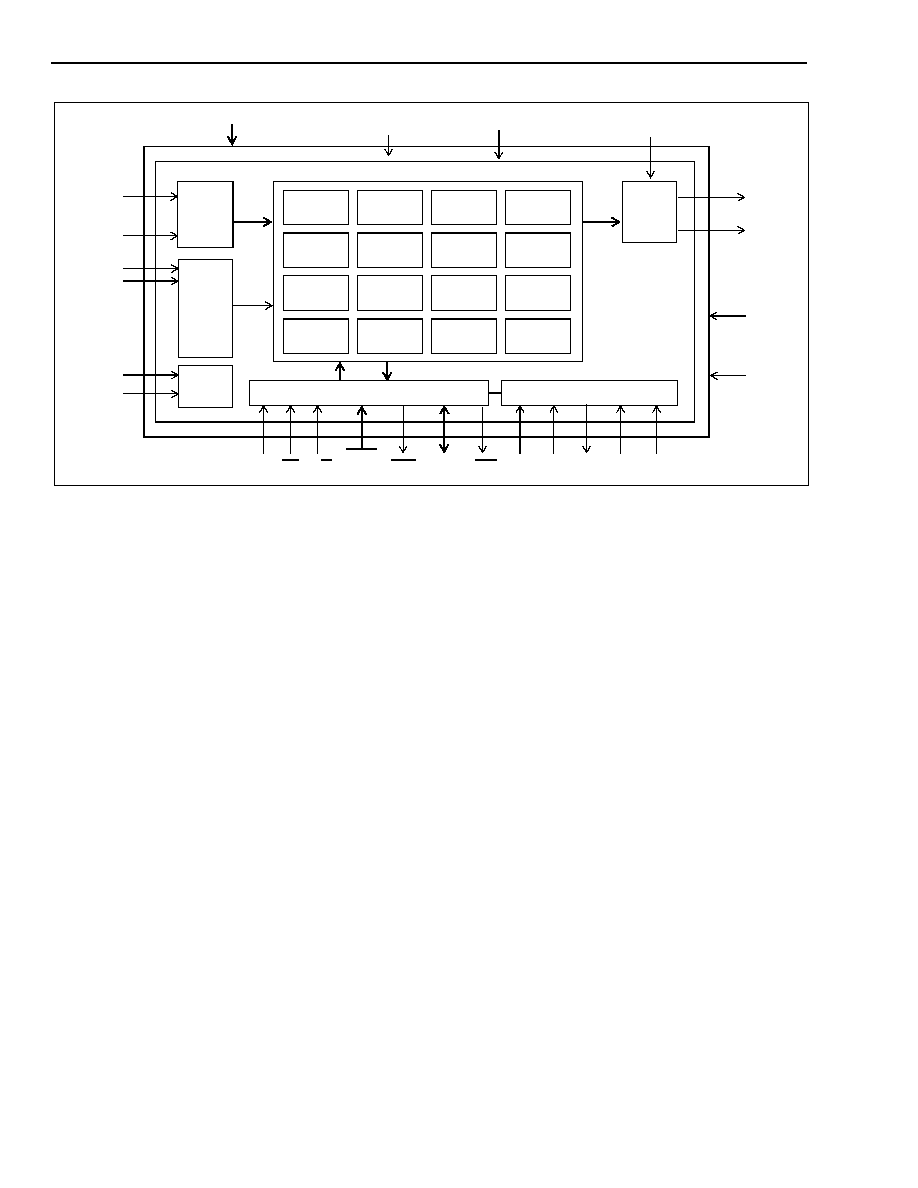
Figure 1 - Functional Block Diagram for single MT93L00 (32 channels)
Features of Single MT93L00
∑
Independent multiple channels of echo cancellation; from 32 channels of 64ms to 16 channels of 128ms
with the ability to mix channels at 128ms or 64ms in any combination
∑
Independent Power Down mode for each group of 2 channels for power management
∑
ITU-T G.165 and G.168 compliant
∑
Field proven, high quality performance
∑
Compatible to ST-BUS and GCI interface at 2Mb/s serial PCM
∑
PCM coding,
µ
/A-Law ITU-T G.711 or sign magnitude
∑
Per channel Fax/Modem G.164 2100Hz or G.165 2100Hz phase reversal Tone Disable
∑
Per channel echo canceller parameters control
∑
Transparent data transfer and mute
∑
Fast reconvergence on echo path changes
∑
Non-Linear Processor with high quality subjective performance
∑
Protection against narrow band signal divergence
∑
Offset nulling of all PCM channels
∑
10 MHz or 20 MHz master clock operation
∑
3.3 V pads and 1.8V Logic core operation with 5-Volt tolerant inputs
∑
No external memory required
∑
Non-multiplexed microprocessor interface
∑
IEEE-1149.1 (JTAG) Test Access Port
RESET
Rout
IC0
Sout
DS CS R/W A10-A0 DTA D7-D0
Echo Canceller Pool
V
SS
V
DD1 (3.3V)
TDI TDO TCK TRST
TMS
Rin
IRQ
C4i
F0i
MCLK
ODE
Sin
Fsel
Test Port
Microprocessor Interface
Timing
Unit
Serial
to
Parallel
Parallel
to
Serial
PLL
Group 0
ECA/ECB
Group 4
ECA/ECB
Group 8
ECA/ECB
Group 12
ECA/ECB
Group 1
ECA/ECB
Group 5
ECA/ECB
Group 9
ECA/ECB
Group 13
ECA/ECB
Group 2
ECA/ECB
Group 6
ECA/ECB
Group 10
ECA/ECB
Group 14
ECA/ECB
Group 3
ECA/ECB
Group 7
ECA/ECB
Group 11
ECA/ECB
Group 15
ECA/ECB
Note:
Refer to Figure 3
for Echo Canceller
block diagram
V
DD2 (1.8V)
Preliminary Information
MT93L04A
3
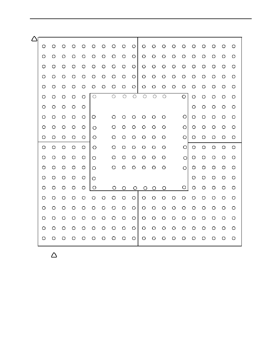
Figure 2 - 365 Ball BGA
B
C
D
E
F
G
H
J
K
L
M
N
1
2
3
4
5
6
7
8
9
10
11
12
13
1
A
14
15
16
P
R
T
U
V
W
Y
17
18
19
20
Tsig(12)_d1
Tsig(0)_d1
Fsel_d4
Tsig(10)_d4
Tsig(14)_d4
SC_fclk_d4
SC_in_d4
SM_mclk_d4
SC_set_d4
Rin_d4
Sout_d4
Tsig(7)_d4
SC_Fclk_d1
SC_in_d1
SM_mclk_d1
FOIB_d1
Rout_d1
Tsig(7)_d1
A_IC2_d1
Tsig(1)_d1
Tsig(15)_d1
A(10)_d1
DT1_d4
Tsig(11)_d4
TM2_d4
SC_reset_d4
ST_mclk_d4
FOIB_d4
Sin_d4
ODE_d4
Tsig(6)_d4
SC_reset_d1
Tsig(2)_d4
Tsig(11)_d1
ST_mclk_d1
SC_set_d1
Sin_d1
ODE_d1
Tsig(6)_d1
Tsig(2)_d1
TM2_d1
A(9)_d1
SG1_d4
Tsig(12)_d4
Tsig(8)_d4
C4IB
Rout_d4
SC_en_d4
Tsig(5)_d4
TD0_d4
Tsig(3)_d4
Tsig(1)_d4
Tsig(13)_d1
Vss
Vss
Vss
Vss
Vss
Vss
Vss
Vss
Vss
Vss
Vss
Vss
Vss
Vss
Vss
Vss
Vss
Vss
Vss
Vss
Vss
Vss
Vss
Vss
Vss
Vss
Vss
Vss
Vss
Vss
Vss
Vss
Vss
Vss
Vss
Vss
Vdd1
Vdd1
Vdd1
Vdd1
Vdd1
Vdd1
Vdd1
Vdd1
Vdd1
Vdd1
Vdd1
Vdd2
Vdd2
Vdd2
Vdd2
Vdd2
Vdd2
Vdd2
Vdd2
Vdd2 Vdd2
Vdd2
Vdd2
Vdd2
Vdd2
Vdd2
Vdd2
Tsig(9)_d1
Fsel_d1
Halt_d1
PLLVDD_d1
AT1_d1
Test_En_d1
TCK_D1
TRSTB_D1
Tm1_d1
Mclk_d1
Step_d1
PLLVSS2_d1
Dsb_d1
TD0_d1
RESETB_d1
Tsig(10)_d1
DT1_d1
Tsig(14)_d1
PLLVSS1_d1
R/WB_d1
TDI_d1
CSB_d1
DTAB_d1
D(1)_d1
TMS_d1
IRQB_d1
D(0)_d1
D(2)_d1
D(3)_d1
D(4)_d1
D(5)_d1
D(6)_d1
SG1(d1)
D(7)_d1
A(1)_d1
A(3)_d1
A(5)_d1
A(6)_d1
A_IC1_d1
A(0)_d1
A(2)_d1
A(4)_d1
Rin_d1
A(7)_d1
A(8)_d1
Tsig(4)_d1
Tsig(8)_d1
Tsig(3)_d1
SC_en_d1
C4IB
Sout_d1
Tsig(5)_d1
Tm1_d4
Tsig(13)_d4
Tsig(15)_d4
Tsig(9)_d4
Mclk_d4
Halt_d4
PLLVSS1_d4
AT1_d4
TMS_d4
A_IC1_d4
A(9)_d4
A(2)_d4
A(6)_d4
A(3)_d4
A(10)_d4
A(7)_d4
A(4)_d4
A(1)_d4
A(8)_d4
A(5)_d4
A(0)_d4
D(4)_d4
D(3)_d4
D(2)_d4
D(0)_d4
D(5)_d4
D(6)_d4
D(7)_d4
D(1)_d4
Csb_d4
DTAB_d4
Dsb_d4
R/WB_d4
Test_en_d4
TCK_d4
IRQB_d4
RESETB_d4
A_IC2_d4
Trstb_d4
Step_d4
PLLVDD_d4
PLLVSS2_d4
TDI_d4
Tsig(4)_d4
Tsig(0)_d4
Sout_d3
ODE_d3
Rout_d3
Tsig(2)_d3
Tsig(0)_d3
Tsig(1)_d3
Tsig(3)_d3
Tsig(7)_d3
Rin_d3
A(9)_d3
A(6)_d3
A(3)_d3
A(2)_d3
D(4)_d3
A(7)_d3
A(5)_d3
A(1)_d3
A(4)_d3
A(0)_d3
A_ICI_d3
D(1)_d3
D(5)_d3
D(7)_d3
D(3)_d3
DTAB_d3
D(6)_d3
D(2)_d3
FOIB_d3
C4IB_d3
SM_mclk_d3
Sin_d3
Tsig(5)_d3
Tsig(6)_d3
Tsig(4)_d3
A_IC2_d3
A(8)_d3
A(10)_d3
ST_mclk_d3
SC_set_d3
SC_in_d3
SC_en_d3
SC_reset_d3
Tsig(10)_d3
Tsig(9)_d3
Tsig(8)_d3
SC_fclk_d3
CSB_d3
D(0)_d3
DSB_d3
IRQB_d3
Tsig(11)_d3
Tsig(13)_d3
Tsig(15)_d3
Tsig(14)_d3
Tsig(12)_d3
R/WB_d3
RESETB_d3
Trstb_d3
Test_en_d3
TCK_d3
TDO_d3
Tm2_d3
TDI_d3
TMS_d3
Halt_d3
Fsel_d3
AT1_d3
PLLVSS2_d3
PLLVDD_d3
PLLVSS1_d3
Step_d3
Mclk_d3
DT1_d3
SG1_d3
TM1_d3
A(5)_d2
A(4)_d2
A(7)_d2
A(8)_d2
A(10)_d2
A(6)_d2
A(0)_d2
A(1)_d2
A(2)_d2
A(3)_d2
A(9)_d2
A_IC1_d2
D(7)_d2
D(6)_d2
D(5)_d2
D(4)_d2
D(3)_d2
D(2)_d2
Tsig(0)_d2
A_IC2_d2
D(1)_d2
D(0)_d2
R/WB_d2
DTAB_d2
Tsig(1)_d2
Tsig(3)_d2
Tsig(4)_d2
Tsig(6)_d2
Tsig(7)_d2
Tsig(13)_d2
Tsig(10)_d2
Tsig(9)_d2
Tsig(5)_d2
Irqb_d2
Test_en_d2
DSB_d2
Csb_d2
Sout_d2
SC_in_d2
SC_set_d2
Tsig(11)_d2
Tsig(14)_d2
Tsig(15)_d2
DT1_d2
Fsel_d2
PLLVSS1_d2
TDI_d2
PLLVDD_d2
Step_d2
Mclk_d2
TM1_d2
Tsig(12)_d2
FOIB_d2
SC_reset_d2
Sin_d2
C4IB_d2
SM_mclk_d2
SC_en_d2
SC_Fclk_d2
Tsig(8)_d2
ST_mclk_d2
Rin_d2
Rout_d2
Ode_d2
TM2_d2
SG1_d2
Halt_d2
PLLVSS2_d2
AT1_d2
TD0_d2
Tck_d2
RESETB_d2
Trstb_d2
Tms_d2
Tsig(2)_d2
Vdd1
Vdd1
1
2
3
4
5
6
7
8
9
10
11
12
13
14
15
16
17
18
19
20
B
C
D
E
F
G
H
J
K
L
M
N
A
P
R
T
U
V
W
Y
1
2
3
4
5
6
7
8
9
10
11
12
- A1 corner is identified by metallized markings.
MT93L04A
Preliminary Information
4
Pin Description
Signal Name
Signal Type
BGA Ball #
Signal Description
V
DD1
= 3.3V
Power
R6, R8, R13, R15, N15,H15,
F15,F13,F8,F6,H6,N6, P6,
Positive Power Supply. Nominally 3.3 volt.
V
DD1
= I/O Voltage
V
DD2
= 1.8V
Power
R9,R10,R11,R12,M15,
L15,K15,J15,F12,F11,
F10,F9,J6, K6, L6,M6,
Positive Power Supply. Nominally 1.8 volt.
V
DD2
= Core Voltage
VSS
Power
H8,H9,H10,H11,H12, H13,
J8, J9,J10,J11,
J12,J13,K8,K9,K10,K11,K1
2,K13 L8,L9,L10,
L11,L12,L13,M8,M9,M10,M
11,M12, M13, N8,
N9,N10,N11,N12,N13
Ground
DEVICE 1
TMS_d1
User Signal
J4
Test Mode Select (3.3V Input).
JTAG signal that
controls the state transitions of the TAP controller.
This pin is pulled high by an internal pull-up when
not driven.
TDI_d1
User Signal
J3
Test Serial Data In (3.3V Input).
JTAG serial test
instructions and data are shifted in on this pin.
This pin is pulled high by an internal pull-up when
not driven.
TDO_d1
User Signal
J2
Test Serial Data Out (Output).
JTAG serial data
is output on this pin on the falling edge of TCK.
This pin is held in high impedance state when
JTAG scan is not enabled.
TCK_d1
User Signal
J1
Test Clock (3.3V Input).
Provides the clock to the
JTAG test logic.
TRSTB_d1
User Signal
K1
Test Reset (3.3V Input).
Asynchronously
initializes the JTAG TAP controller by putting it in
the Test-Logic-Reset state. This pin should be
pulsed low on power-up or held low, to ensure that
the MT93L00 is in the normal functional mode.
This pin is pulled by an internal pull-down when
not driven.
Test_En_d1
ICO
H1
Internal Connection.
Connected to VSS for
normal operation
RESETB_d1
User
Signal
K2
Device Reset (Schmitt Trigger Input).
An active
low resets the device and puts the MT93L00 into a
low-power stand-by mode.
When the RESET pin is returned to logic high
and a clock is applied to the MCLK pin, the
device will automatically execute initialization
routines, which preset all the Control and Status
Registers to their default power-up values.

Preliminary Information
MT93L04A
5
IRQB_d1
User Signal
J5
Interrupt Request (Open Drain Output).
This
output goes low when an interrupt occurs in any
channel. IRQ returns high when all the interrupts
have been read from the Interrupt FIFO Register.
A pull-up resistor (1K typical) is required at this
output.
DSB_d1
User Signal
H2
Data Strobe (Input).
This active low input works
in conjunction with CS to enable the read and
write operations.
CSB_d1
User Signal
K3
Chip Select (Input).
This active low input is used
by a microprocessor to activate the
microprocessor port.
R/WB_d1
User Signal
H3
Read/Write (Input).
This input controls the
direction of the data bus lines (D7-D0) during a
microprocessor access.
DTAB_d1
User Signal
K4
Data Transfer Acknowledgment (Open Drain
Output).
This active low output indicates that a
data bus transfer is completed. A pull-up resistor
(1K typical) is required at this output.
D(0)_d1
User Signal
H4
Data Bus D0 - D7 (Bidirectional).
These pins
form the 8-bit bidirectional data bus of the
microprocessor port.
D(1)_d1
User Signal
K5
D(2)_d1
User Signal
H5
D(3)_d1
User Signal
G4
D(4)_d1
User Signal
G5
D(5)_d1
User Signal
F4
D(6)_d1
User Signal
F5
D(7)_d1
User Signal
E5
A(0)_d1
User Signal
D4
Address A0 to A10 (Input).
These inputs provide
the A10 - A0 address lines to the internal
registers.
A(1)_d1
User Signal
E6
A(2)_d1
User Signal
D5
A(3)_d1
User Signal
E7
A(4)_d1
User Signal
D7
A(5)_d1
User Signal
E8
A(6)_d1
User Signal
E10
A(7)_d1
User Signal
D8
A(8)_d1
User Signal
D10
A(9)_d1
User Signal
C10
A(10)_d1
User Signal
B10
A_IC1_d1
ICO
E9
Internal Connection.
Connected to VSS for
normal operation
A_IC2_d1
ICO
A8
Internal Connection.
Connected to VSS for
normal operation
Pin Description (continued)
Signal Name
Signal Type
BGA Ball #
Signal Description