 | –≠–ª–µ–∫—Ç—Ä–æ–Ω–Ω—ã–π –∫–æ–º–ø–æ–Ω–µ–Ω—Ç: MV1442 | –°–∫–∞—á–∞—Ç—å:  PDF PDF  ZIP ZIP |

Obsolescence Notice
This product is obsolete.
This information is available for your
convenience only.
For more information on
Zarlink's obsolete products and
replacement product lists, please visit
http://products.zarlink.com/obsolete_products/
Features
∑ On-chip Digital Clock Regenerator
∑ HDB3 Encoding and Decoding to CCITT
Recommendation G.703
∑ Asynchronous Operation
∑ Simultaneous Encoding and Decoding
∑ Clock Recovery Signal allows Off-chip Clock
Regeneration
∑ Loop Back Control
∑ HDB3 Error Monitor
∑ `All Ones' Error Monitor
∑ Loss of Input Alarm
∑ Low Power Operation
∑ 2.048MHz or 1.544MHz Operation in External or
Internal Clock Recovery mode
∑ 8.448MHz Operation in External Clock Recovery
mode
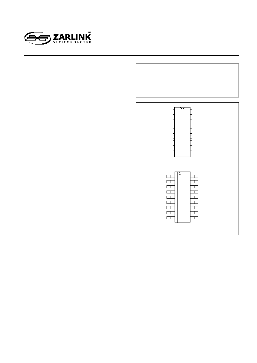
Figure 1 - Pin connections ≠ top view
-0.5V to +7V
V
DD
-0.5V to GND -0.5V
V
DD
-0.5V to GND -0.5V
-55
∞C to +125∞C
Absolute Maximum Ratings
V
DD
Inputs
Outputs
Storage temperature
MV1442
HDB3 Encoder/Decoder/Clock Regenerator
DS3077
ISSUE 4.0
July 2001
Ordering Information
MV1442/IG/DPAS DIL plastic package
MV1442/IG/MPES Miniature plastic package
MV1442/IG/MPEG Miniature plastic (tape and reel)
The MV1442, along with other devices in the Zarlink 2Mbit
PCM signalling series comprise a group of circuits which will
perform the common channel signalling and error detection
functions for a 2.048Mbit PCM transmission link operating in
accordance with the appropriate CCITT recommendations.
The circuits are fabricated in CMOS and operate from a
single +5V supply with all inputs and outputs being TTL
compatible.
The MV1442 is an encoder/decoder for the HDB3 pseudo-
ternary transmission code, described in Annex A of CCITT
Recommendation G.703. The device encodes and decodes
simultaneously and asynchronously. Error monitoring
functions are provided to detect violations of the HDB3
coding, all ones detection and loss of input (all zeros detection)
In addition a loop back function is provided for terminal
testing. The MV1442 may be selected to function in either
internal or external clock recovery modes. Internal clock
recovery mode may be selected tor either 1.544MHz or
2.048MHz operation and in this mode an external 16.384MHz
crystal (12.352MHz for 1.544MHz operation) is required.
External clock recovery mode may be selected for 1.544MHz,
2.048MHz or 8.448MHz operation.
NRZ DATA IN
ENCODER CLOCK
LOSS OF INPUT
NRZ DATA OUT
DECODER CLOCK
RESET AIS
AIS
MODE
GND
18
17
16
15
14
13
12
11
10
1
2
3
4
5
6
7
8
9
V
DD
TXD2
TXD1
RXD2
LOOP TEST ENABLE
RXD1
CRYSTAL OUT/CDR
DOUBLE VIOLATION
CRYSTAL IN
1
2
3
4
5
6
7
8
9
18
17
16
15
14
13
12
11
10
NRZ DATA IN
ENCODER CLOCK
LOSS OF INPUT
NRZ DATA OUT
DECODER CLOCK
RESET AIS
AIS
MODE
GND
V
DD
TXD2
TXD1
RXD2
LOOP TEST ENABLE
RXD1
CRYSTAL OUT/CDR
DOUBLE VIOLATION
CRYSTAL IN
DP18
MP18
(WIDE BODY)
2
MV1442
CLOCK
REGENERATOR
CRYSTAL
OUT/CDR
CRYSTAL
IN
ENCODER
NRZ
DATA IN
ENCODER
CLOCK
CLOCK
REGENERATOR
DECODER
ERROR
CIRCUIT
COUNTER
AIS CIRCUIT
MODE
RXD 1
LOOP TEST
ENABLE
RXD 2
TXD 1
TXD 2
DOUBLE VIOLATION
DECODER
CLOCK
LOSS OF
INPUT
NRZ DATA
OUT
AIS
RESET AIS
Functional Descriptions
High Density Bipolar 3 (HDB3) is a pseudo-ternary trans-
mission code in which the number of consecutive zeros
which may occur is restricted to three to allow adequate
clock recovery at the receiver. In any sequence of four
consecutive binary zeros the last zero is substituted by a
mark of the same polarity as the previous mark, thus break-
ing the Alternate Mark Inversion (AMI) code. This mark is
termed a violation. In addition, the first zero may also be
substituted by a mark if the last mark and last violation are of
the same polarity. This mark does not violate the AMI code
and ensures that successive violations alternate in polarity
and as such introduce no DC component to the HDB3 signal.
The MV1442 consists of three main blocks: the HDB3
Encoder, the HDB3 Decoder and the Clock Regenerator.
The function of each block is now described separately.
HDB3 Encoder
The HDB3 Encoder is responsible for converting the
incoming NRZ data into pseudo-ternary form for transmis-
sion over a PCM link. This conversion is carried out in
accordance with the HDB3 coding laws specified in CCITT
Recommendation G. 703 The data to be encoded is input on
the NRZ DATA IN pin and the encoding process is synchro-
nised to the clock signal being input on the ENCODER
CLOCK pin. The two TXD outputs TXD1 and TXD2. repre-
sent the HDB3 data in pseudo-ternary form. If a mark is to be
transmitted, the output goes high after the rising edge of the
clock. The length of the pulse is set by the positive clock
pulse width. The timing diagram of the HDB3 Encoder is
shown in Figure 3.
HDB3 Decoder
The HDB3 Decoder is responsible for decoding the HDB3
pseudo-ternary data on its inputs RXD1 and RXD2 into NRZ
form to be output on the NRZ DATA OUT pin. In addition to
this, the decoder circuit provides three alarm outputs. The
first of these alarms is DOUBLE VIOLATION. As its name
suggests, a logic high on this output denotes that two
successive violations have been received with the same
polarity, thus violating the HDB3 coding laws. The second
alarm, LOSS OF INPUT, is used to denote that 11 consecu-
tive zeros have been received on the RXD inputs. The final
alarm output is AIS (all ones) This alarm goes high if less
than 3 decoded zeros have been detected in the preceding
RESET AIS = 1 period (i.e. between RESET AIS = 0 pulses)
and as such this alarm can be used as an `all ones' detector.
The decoding process and all the alarm circuitry is synchro-
nised to the clock signal being input to this block on the
DECODER CLOCK pin. This clock signal may be asynchro-
nous with the ENCODER CLOCK signal. The timing dia-
grams of the HDB3 Decoder and alarm circuitry are shown
in Figures 4 to 7.
In addition to the normal mode of operation, a loop test
mode is available for terminal testing. This mode is selected
by taking the LOOP TEST ENABLE input high. In this mode
the HDB3 encoded pseudo-ternary data outputs of the
Encoder block are fed back as the inputs to the Decoder
block, which in turn decodes this data and outputs it in NRZ
form.
Clock Regenerator
The Clock Regenerator block has two possible modes of
operation. With the MODE pin high, internal crystal control-
led clock regeneration is selected, whereas with the MODE
pin low external clock regeneration is selected using, for
example, a tuned circuit.
In external clock regeneration mode, a logically ORed
version of the HDB3 data, from the RXD inputs, is output to
the external clock regeneration circuitry on the CRYSTAL
OUT/CDR pin. The regenerated clock is then fed back into
the MV1442 on the DECODER CLOCK pin External clock
regeneration may be used for operation with data rates of
1.544Mbits, 2.048Mbits or 8.448Mbits.
In internal clock regeneration mode, the logically ORed
data is input to a digital regenerator which constantly
resynchronises a divide-by-8 counter to the incoming data
stream. The clock thus regenerated is output to the de-
coder circuitry and to any external circuitry on the
DECODER CLOCK pin. A crystal of frequency 8 times the
required data rate must be connected between the
CRYSTAL IN and CRYSTAL OUT/CDR pins. Thus, the
crystal frequency needs to be 16.384MHz or 12.352MHz
for data rates of 2.048Mbits or 1.544Mbits respectively.
Internal clock regeneration may not be used for operation
at a data rate of 8.448Mbits.
The MV1442 is capable of withstanding up to 0.25UI of
peak to peak input jitter at a jitter frequency of 2.048MHz
without introducing errors into the decoded data. At lower
jitter frequencies the MV1442 is capable of withstanding
much larger values to peak to peak input jitter. In the
Figure 2 - Block diagram
3
MV1442
B
B
B
V
4∑5 CLOCK PERIODS
B
B
V
ENCODER
CLOCK
NRZ DATA IN
TXD1
TXD2
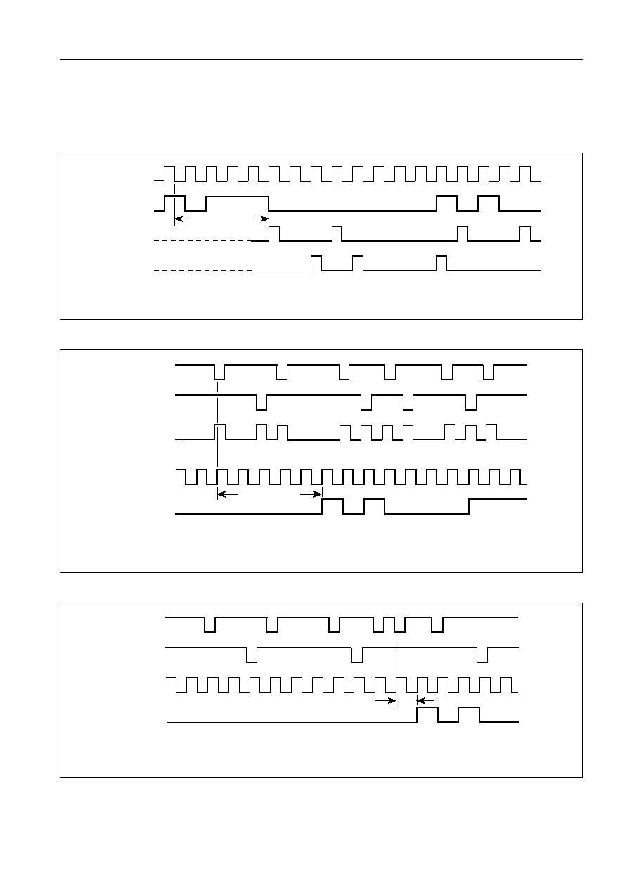
NOTES
1. The encoded HDB3 outputs, TXD1 and TXD2. are delayed dy 4∑5 clock periods with respect to NRZ DATA IN.
2. B is an HDB3 mark, V is an HDB3 violation.
Figure 3 - Encoder waveforms
B
B
V
B
B
B
B
B
B
B
5 CLOCK PERIODS
RXD1
RXD2
NRZ DATA OUT
CDR
DECODER
CLOCK
NOTES
1. The decoded NRZ output is delayed by 5 clock periods with respect to the HDB3 inputs.
2. The diagram assumes the last violation occured on RXD2.
3. B is an HDB3 mark, V is an HDB3 violation.
Figure 4 - Decoder waveforms
B
B
V
B
V
B
B
B
1 CLOCK PERIOD
RXD1
RXD2
DECODER
CLOCK
NOTES
1. There is a single clock period delay from detection of an error and the rising edge of DOUBLE VIOLATION
2. The diagram assumes the last violation occured on RXD2.
3. B is an HDB3 mark, V is an HDB3 violation.
V
DOUBLE
VIOLATION
Figure 5 - HDB3 double violation waveforms
absence of input jitter the MV1442 will produce an output
jitter waveform in the form of a sawtooth ramping between
0UI and 0.125UI. The period of this waveform will be de-
pendent upon the difference in frequencies between the
remote transmitter's clock and the crystal controlled clock of
the MV1442.
The MV1442 was originally designed as a pin compatible
replacement for the MV1441 with a much improved internal
clock recovery circuit and allowing operation at 8.448MHz
with external clock recovery selected.
4
MV1442
1 CLOCK PERIOD
RXD1
RXD2
DECODER
CLOCK
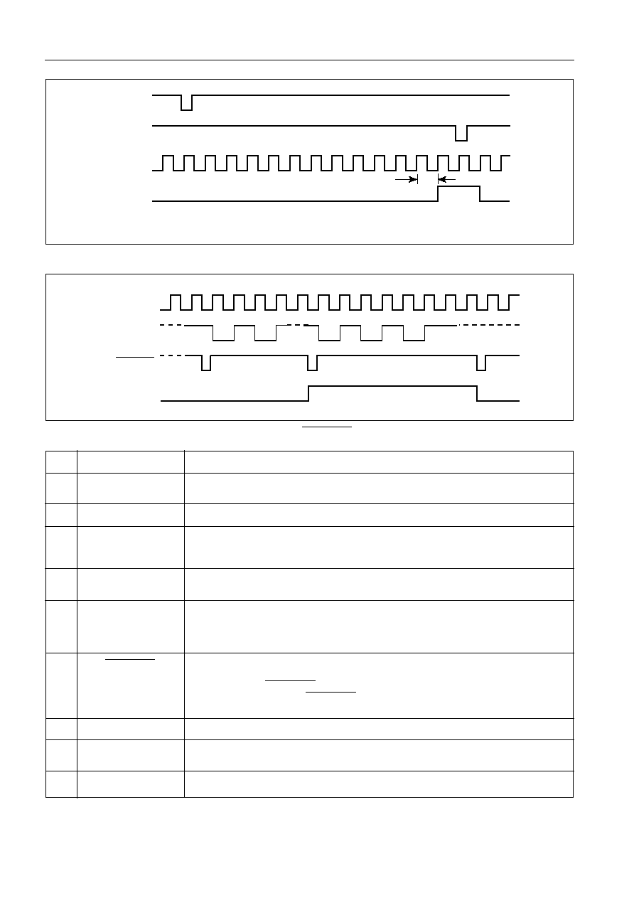
NOTE
The LOSS OF INPUT output is delayed by one clock period with respect to the incoming HDB3 waveform
LOSS OF
INPUT
1
2
3
4
5
6
7
8
9
10
11
Figure 6 - Loss of input waveforms
1
2
3
4
5
6
7
8
9
Pin
Signal name
Description
NRZ DATA IN
ENCODER CLOCK
LOSS OF INPUT
NRZ DATA OUT
DECODER CLOCK
RESET AIS
AIS
MODE
GND
Input pin for data to be encoded into pseudo-ternary HDB3 form. This data is clocked into
the Encoder block by the falling edge of ENCODER CLOCK.
Clock input for the encoding of data on pin 1.
Output from the loss of input circuit This output goes high one clock period after the
detection of eleven consecutive zeros on the decoder inputs. Any logic `1' at the input
(RXD1 or RXD2=0) resets this count after a single clock period delay.
NRZ data output obtained from the decoding of the pseudo-ternary inputs to the Decoder
block.
Clock input to the Decoder block for decoding data on RXD1 and RXD2 or TXD1 and TXD2
in loop test mode. In internal clock regeneration mode, this pin is used to output the
regenerated clock to external circuitry. In external clock regeneration, mode this pin is
used to input the externally regenerated clock signal direct to the Decoder block.
Reset input to the decoded zero counter A logic `0' on this input resets a decoded zero
counter. It will also reset the AIS output to `0' provided 3 or more zeros have been decoded
in the preceding RESET AIS = 1 period or set AIS to 1 if less than 3 zeros have been
decoded in the preceding RESET AIS = 1 period This may be used to indicate loss of
timeslot zero. A logic `1' on this pin enables the decoded zero counter.
Output from AIS circuit (see description for pin 6).
Input pin for selection of clock regeneration mode. A logic high on this input selects internal
crystal controlled clock regeneration while a logic low selects external clock regeneration.
Digital ground 0V.
Table 1 - Pin descriptions
Contd...
DECODER
CLOCK
NRZ DATA OUT
RESET AIS
AIS
Figure 7 - AIS and RESET AIS waveforms