The PDSP16488A is a fully integrated, application specific,
image processing device. It performs a two dimensional convo-
lution between the pixels within a video window and a set of
stored coefficients. An internal multiplier accumulator array can
be multi-cycled at double or quadruple the pixel clock rate. This
then gives the window size options listed in Table 1.
An internal 32kbit RAM can be configured to provide either
four or eight line delays. The length of each delay can be
programmed to the users requirement, up to a maximum of 1024
pixels per line. The line delays are arranged in two groups,which
may be internally connected in series or may be configured to
accept separate pixel inputs. This allows interlaced video or
frame to frame operations to be supported.
The 8-bit coefficients are also stored internally and can be
downloaded from a host computer or from an EPROM. No
additional logic is required to support the EPROM and a single
device can support up to 16 convolvers.
The PDSP16488A contains an expansion adder and delay
network which allows several devices to be cascaded. Con-
volvers with larger windows can then be fabricated as shown in
Table 2.
Intermediate 32-bit precision is provided to avoid any danger
of overflow, but the final result will not normally occupy all bits.
The PDSP16488A thus provides a gain control block in the
output path, which allows the user to align the result to the most
significant end of the 32-bit word.
Table 2 PDSP16488As needed to implement typical window sizes
Pixel
size
Width
Window size
Depth
Maximum pixel
rate (MHz)
Line delays
8
8
8
16
16
4
8
8
4
8
4
4
8
4
4
20
20
10
20
10
431024
431024
83512
43512
43512
Table 1 Single PDSP16488A configurations
Max.
pixel
rate
(MHz)
Pixel
size
3 3 3 5 3 5 7 3 7 9 3 9 11311 15315 23323
No. of PDSP16488As for N3N window size
10
10
20
20
40
40
8
16
8
16
8
16
1
1
1
1
1
2
1
2
2
4
4*
-
1
2
2
4
4*
-
4
-
6
-
-
-
4
-
6
-
-
-
4
-
8
-
-
-
9
-
-
-
-
-
*Maximum rate is limited to 30MHz by line store expansion delays
ORDERING INFORMATION
Commercial (0
�
C to 170
�
C)
PDSP16488A / C0 / AC (PGA)
Industrial (240
�
C to 185
�
C)
PDSP16488A / B0 / AC (PGA)
PDSP16488A / B0 / GC (QFP)
Military (255
�
C to 1125
�
C)
PDSP16488A / A0 / AC (PGA)
PDSP16488A / A0 / GC (QFP)
PDSP16488A / MA / ACBR (PGA) MIL-STD-883 Class B*
PDSP16488A / MA / GCPR (QFP) MIL-STD-883 Class B*
*
See Notes following Static Electrical CharacteristicsTable
Note:
PDSP16488A devices are not guaranteed to cascade with
PDSP16488 devices. Zarlink Semiconductor do not recommend
that PDSP16488A be mixed with PDSP16488 devices in a single
equipment design. The PDSP16488A requires external pullup
resistors in EPROM Mode (see Static Electrical Characteristics).
FEATURES
s
The PDSP16488A is a replacement for the
PDSP16488 (see Note below)
s
8 or 16-bit Pixels with rates up to 40 MHz
s
Window Sizes up to 838 with a Single Device
s
Eight Internal Line Delays
s
Supports Interlace and Frame-to-Frame Operations
s
Coefficients Supplied from an EPROM or Remote Host
s
Expandable in both X and Y for Larger Windows
s
Gain Control and Pixel Output Manipulation
s
84-pin PGA or 132-pin QFP Package Options
Fig. 1 Typical stand-alone real time system
PDSP16488A
EPROM
ADDR
DATA
POWER
ON
RESET
DELAYED
SYNC
OUTPUT
DATA
RES
DELOP
CLK
HRES
BYPASS
SYNC
EXTRACT
COMPOSITE
DATA
PIXEL
CLOCK
GEN
ADC
OPTIONAL
FIELD
DELAY
IP7:0
L7:0
D15:0
SYNC
ODD FIELD
PDSP16488A
Single Chip 2D Convolver with Integral Line Delays
Advance Information
DS3713
ISSUE 6.4
December 1997
PDSP16488A
2
Type
Input
I/O
Input
Input
Dual
function
Output
Output
Input
Output
I/O
Input
Input
I/O
Input
Output
Output
Input
Input
Input
Input
Outputs
Outputs
Power
Power
Signal
IP7:0
L7:0
BYPASS
HRES
X15:0
D15:0
PC1
PC0
DELOP
DS
CE
R/W
PROG
CLK
BIN
OVR
RES
S I N G L E
MASTER
OEN
CS3:0
F1:0
V
DD
GND
Table 3 Signal descriptions
Description
Pixel data input to the first line delay (most significant byte in 16-bit mode).
Pixel data input to the second group of line delays. (least significant byte in 16-bit mode). Alterna-
tively an output from the last line delay when the appropriate mode bit is set.
The first line delay in the first group is bypassed when this input is high. No internal pullup resistor.
Resets the line delay address pointers when high. Normally the composite sync signal in real time
applications. In non real time systems it defines a frame store update period, when low.
Address/data connections from a Master or Single device to the external coefficient source,
with X15 defining EPROM or Host support. Otherwise they provide the expansion data input.
Signed 16-bit scaled data or multiplexed 32-bit intermediate data. During intermediate transfers the
most significant half is valid when the clock is low, and the least significant half when clock is high.
During programming a Master device outputs a timing strobe on this pin. This is passed down
the chain in a multiple device system, using the
PC0
input on the next device.
This pin is used in conjunction with
PC1
in multiple device systems. It terminates the write strobe
from a Master device which is EPROM supported.
This output provides a version of the HRES input which has been delayed by an amount defined by
the user.
The data strobe from a host computer, active low. This pin will be an output from an EPROM
supported Master device which provides strobes to the remaining devices.
An active low enable which is internally gated with
R/W
and
DS
to perform reads or writes to the
internal registers. In a Single or Master device, which is supported from an EPROM, the
bottom 72 addresses are always used and
CE
is not needed.
CE
can then be used to initiate a
new register load sequence after the power on load sequence.
Read / not write line from the host CPU. When an EPROM is used this pin should be tied low.
This pin is normally an input which signifies that registers are to be changed or examined. It is,
however, an output from an EPROM supported Single or Master device indicating to the rest
of the system that registers are being updated.
Clock. All events are triggered on the rising edge of CLK, except the latching of least significant
expansion inputs . Internally the clock can be multiplied by two or four in order to increase the
effective number of multipliers.
This output indicates the result from the internal comparison. A high value indicates that the pixel
was greater than the internal threshold. The output is only valid from the last device in a chain.
When high this output indicates that there has been a gain control overflow.
Active low power on reset signal.
Tied to ground to indicate a Single device system. Internal pullup resistor.
Tied to ground to indicate the Master device in a multiple device system. Must be left open circuit
in a Single device system. Internal pullup resistor.
Output enable signal. Active low.
Four address bits from a Master specifying one of sixteen devices in a multiple device system.
Must be externally decoded to provide chip enables for the additional devices.
These bits indicate the field selection given by the gain control auto select logic. The same coding
as that used for Control Register bits C5:4 is used.
15V supply. All V
DD
pins must be connected.
0V supply. All GND pins must be connected.
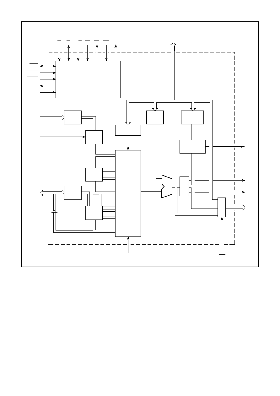
PDSP16488A
3
ADDER
8
3
8
ARRAY
OF
MACs
COEFFICIENT
STORE (64)
3 LINE
DELAYS
4 LINE
DELAYS
1 LINE
DELAY
Y
DELAY
Y
DELAY
BYPASS
X
DELAY
CS3:0
RES
CONTROL
PC1
CONTROL
REGISTERS
COMPARATOR
MUX
D15:0
BIN
OVR
CLK
OEN
PROG
MASTER
SINGLE
DELOP
HRES
PC0
R / W
DS
CE
BIDIRECTIONAL
MULTIPURPOSE
DATA BUS X15:0
IP7:0
L7:0
GAIN
CONTROL
F1:0
Fig. 2 Functional block diagram
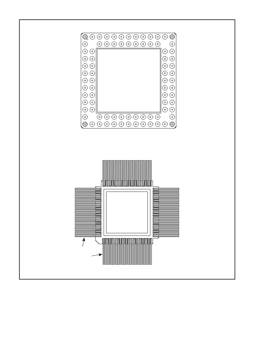
PDSP16488A
4
A B
C D E
F
G H J K L
M
N
1
2
3
4
5
6
7
8
9
10
11
12
13
PIN 1
PIN 132
Fig. 3a Pin connections for 84 I/O pin grid array package - AC84 (Power ) (bottom view)
Fig 3b Pin connections for 132 I/O ceramic power flatpack - GC132 (Power) (top view)
Fig 3 Pin connection diagrams (not to scale). See Table 3 for signal descriptions and Tables 4 and 5 for pinouts.
PDSP16488A
5
Pin
1
2
3
4
5
6
7
8
9
10
11
12
13
14
15
16
17
18
19
20
21
22
23
24
25
26
27
28
29
30
31
32
33
Pin
34
35
36
37
38
39
40
41
42
43
44
45
46
47
48
49
50
51
52
53
54
55
56
57
58
59
60
61
62
63
64
65
66
Signal
N/C
D0
OEN
BIN
PC1
V
DD
GND
OVR
N/C
HRES
R/W
CE
N/C
N/C
GND
N/C
DS
GND
V
DD
PROG
GND
CS3
CS2
CS1
CS0
V
DD
RES
PC0
N/C
DELOP
X0
X1
N/C
Signal
N/C
X2
X3
X4
N/C
X5
GND
X6
X7
N/C
X8
X9
V
DD
V
DD
V
DD
X10
MASTER
N/C
X11
X12
S I N G L E
GND
GND
N/C
X13
X14
N/C
X15
V
DD
BYPASS
IP0
V
DD
N/C
Pin
67
68
69
70
71
72
73
74
75
76
77
78
79
80
81
82
83
84
85
86
87
88
89
90
91
92
93
94
95
96
97
98
99
Signal
N/C
IP1
GND
IP2
N/C
V
DD
IP3
V
DD
IP4
GND
IP5
GND
IP6
V
DD
IP7
V
DD
N/C
L7
GND
L6
GND
L5
V
DD
L4
V
DD
L3
V
DD
L2
GND
L1
F1
L0
N/C
Pin
100
101
102
103
104
105
106
107
108
109
110
111
112
113
114
115
116
117
118
119
120
121
122
123
124
125
126
127
128
129
130
131
132
Signal
N/C
V
DD
F0
D15
N/C
D14
D13
GND
D12
GND
V
DD
V
DD
D11
D10
D9
GND
CLK
CLK
CLK
GND
GND
D8
V
DD
D7
D6
D5
D4
GND
D3
N/C
D2
D1
N/C
Table 5 Pin connections for GC132 (power) package. See Fig 3b.
Pin
A1
B1
C2
C1
D2
D1
E2
E1
F2
G2
G1
H2
J1
J2
K1
K2
L1
Signal
L0
F1
L1
L2
L3
N/C
L4
L5
L6
L7
IP7
N/C
IP6
IP5
IP4
N/C
IP3
Pin
L2
M1
N1
N2
M3
N3
M4
N4
M5
N5
M6
M7
N7
M8
N9
M9
N10
Signal
IP2
IP1
IP0
BYPASS
X15
X14
X13
N/C
S I N G L E
X12
X11
MASTER
X10
X9
X8
X7
X6
Pin
M10
N11
M11
N12
N13
M13
L12
L13
K12
K13
J12
J13
H12
G12
G13
F12
E13
Signal
X5
X4
X3
X2
X1
X0
DELOP
PC0
RES
CS0
CS1
CS2
CS3
PROG
DS
CE
R/W
Pin
E12
D13
D12
C13
C12
B13
A13
A12
B11
A11
B10
A10
B9
A9
B8
B7
A7
Signal
HRES
OVR
PC1
BIN
OEN
D0
D1
D2
D3
D4
D5
D6
D7
D8
CLK
N/C
D9
Pin
B6
A5
B5
A4
B4
A3
B3
A2
F1
N6
F13
A6
H1
N8
H13
A8
Signal
D10
D11
N/C
D12
D13
D14
D15
F0
V
DD
1
V
DD
2
V
DD
3
V
DD
4
GND1
GND2
GND3
GND4
Table 4 Pin connections for AC84 (power) package. See Fig. 3a.