1
Zarlink Semiconductor Inc.
Zarlink, ZL and the Zarlink Semiconductor logo are trademarks of Zarlink Semiconductor Inc.
Copyright 2003-2004, Zarlink Semiconductor Inc. All Rights Reserved.
Features
� Single chip mixer/oscillator PLL combination for
multi band tuner for DTT applications
� Each mixer oscillator band optimized for wide
dynamic range
� RF input stages allow for either single-ended or
differential drive
� PLL frequency synthesizer designed for low
phase noise performance
� Broadband output level detect with onset adjust
� PLL frequency synthesizer compatible with
standard digital terrestrial offsets
� Four integrated switching ports
� I
2
C fast mode compliant
� ESD protection (Normal ESD handling
procedures should be observed)
Applications
� Terrestrial digital receiver systems
� Terrestrial analogue receiver systems
� Cable receiver systems
� Data communications systems
Description
The SL2610 is a mixer oscillator intended primarily
for application in all band tuners, where it performs
image reject downconversion of the RF channel to a
standard 36 MHz or 44 MHz IF.
Each band consists of a low noise preamplifier/mixer
and local oscillator with an external varactor tuned
tank. The band outputs share a common low
impedance SAWF driver stage.
Frequency selection is controlled by the on-board I
2
C
bus frequency synthesizer. This block also controls
four general purpose switching ports for selecting the
prefilter/AGC stages.
October 2004
Ordering Information
SL2610/IG/LH1Q 40 Pin MLP Tape & Reel, Bake & Drypack
SL2610/IG/LH1N 40 Pin MLP Trays, Bake & Drypack
SL2610/IG/LH2Q 40 Pin MLP Tape & Reel, Bake & Drypack*
SL2610/IG/LH2N 40 Pin MLP Trays, Bake & Drypack*
*Leadfree
-40
�
C to +85
�
C
SL2610
Wide Dynamic Range Image Reject MOPLL
Data Sheet
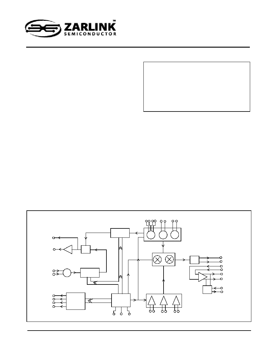
Figure 1 - SL2610 Block Diagram
HI
CONVOP
~
~
~
BAND
LO
BAND
MID
BAND
CONVOPB
IFIP
IFIPB
IFOP
IFOPB
AGC BIAS
AGC OUT
HI
BAND
LO
BAND
MID
BAND
I
2
C
Interface
Port
Interface
REF
DIVIDER
~
PORT P0
PORT P1
PORT P2
PORT P3
PROG
DIVIDER
CHARGE
PUMP
DRIVE
XTAL
XTALCAP
SDA SCL ADD
IF
SELECT
SL2610
Data Sheet
2
Zarlink Semiconductor Inc.
The SL2610 has high intermodulation intercept performance so offering high signal to spurious performance in
the presence of higher amplitude interferers or in the presence of a wide bandwidth composite input signal.
An output broadband level detect circuit is included for control of the tuner front end AGC.
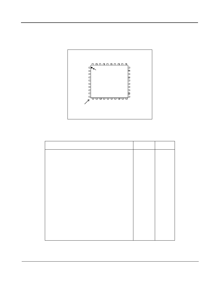
Figure 2 - Pin Allocation Diagram
Quick Reference Data
Characteristics
Units
Frequency range:
LOW band
50-500
MHz
MID band
50-500
MHz
HIGH band
200-900
MHz
Conversion gain *
32
�
2
dB
Noise figure
13
dB
Typical Image Reject
35
dB
P1dB input referred, Converter section only
106
dBuV
IP3 input referred, Converter section only
14
dBm
IP2 input referred, Converter section only
48
dBm
LO phase noise (free running)
@ 10 kHz offset
-90
dBc/Hz
@ 100 kHz offset
-110
dBc/Hz
PLL phase noise
-158
dBc/Hz
Maximum composite output amplitude
3
dBm
* Assuming 2 dB shaping filter loss in external IF path.
LH40
PORT P3
VccRF
HI INPUT
PORT P2
PORT P1
MID INPUT
LOL
O
WOP
LOL
O
WOP
B
LOM
I
DOP
VccL
O
L
O
H
IIP
LOHI
OP
LOHI
OP
B
L
O
H
IIP
B
VccL
O
MID INPUTB
VccRF
LO INPUT
IFOPB
IFOP
AGCBIAS
VCCIF
IFIPB
IFIP
ADD
CONVOP
CONVOPB
VccDIG
LO
I
N
P
U
TB
VccRF
AG
C
O
U
T
PO
R
T
P
0
CH
A
R
G
E
PUMP
XT
AL CAP
DRIVE
XTAL
SDA
SCL
LOM
I
DOP
B
HI INPUTB
VEE
(PACKAGE
PADDLE)
Pin 1
SL2610
Data Sheet
3
Zarlink Semiconductor Inc.
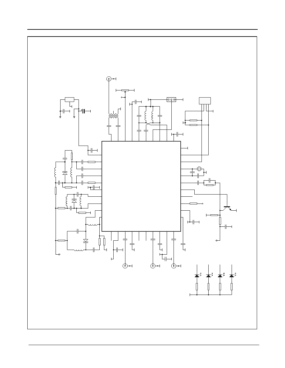
Figure 3 - SL2610 Evaluation Board Schematic
C1
4
2p2
C1
3
2p2
C1
2
2p2
C1
1
2p2
L5
22nH
L6
8n2H
C1
6
100pF
C1
5
5pF
R6
4K7
gnd
SDA
3
VDD
4
GND
5
SCL
6
CN1
I2C
gnd
R1
1
4K7
R1
0
4K7
+5V
C1
7
100nF
C1
9
47pF
C1
8
47pF
X1
4 M
H
z
gnd
C2
0
47pF
R7
33K
TR1
BCW
3
1
gnd
R8
20K
+30V
R9
18K
C2
1
1n5F
gnd
VT
+5V
+5V
+5V
+5V
+5V
+5V
L4
82nH
D2
BB640
C1
0
7pF
L3
36nH
L2
1u5H
C2
6p8F
L1
120nH
D1
BB640
R2
1K
R4
4K7
VT
R5
1K
L7
220nH
L8
220nH
C2
7
82pF
C2
6
82pF
+5V
C2
4
1nF
C2
5
1nF
T1
5:1
SK4
IF OUT
gnd
C3
1nF
C4
1nF
C5
1nF
C6
1nF
C7
1nF
C8
1nF
SK1
HI IN
SK2
MI
D
I
N
SK3
LO
W
IN
gnd
gnd
gnd
R3
1K
gnd
1
2
3
CN2
gnd
+30V
GND
+5V
C2
9
10nF
C3
0
10nF
C3
1
10nF
C3
2
10nF
C3
3
10nF
C3
4
10nF
C3
5
10nF
gnd
C3
6
470uF
+30V
C2
8
100nF
gnd
D4
P0
D5
P1
D6
P2
D7
P3
R1
2
750R
R1
3
750R
R1
4
750R
R1
5
750R
+5V
P0
P1
P2
P3
P0
P1
P2
P3
+5V
C2
2
10nF
C2
3
10nF
1
2
3
CN3
ADDRESS
gnd
C1
100pF
R1
4K7
gnd
gnd
C9
100pF
R1
6
20R
R1
7
10R
R1
8
10R
D3
BB555
R1
9
10R
R2
0
10K
PORT
P3
1
V
cc R
F
2
HIGH IP
3
HIGH IP B
4
PORT
P2
5
PORT
P1
6
MI
D
I
N
P
U
T
7
M
I
D IP B
8
V
cc R
F
9
LO INPUT
10
LO
INPUT B
11
Vcc R
F
12
AGC OUT
13
PORT P0
14
DRIVE
15
CHARGE PUMP
16
XTAL
CAP
17
XTAL
18
SDA
19
SCL
20
V
cc D
I
G
21
CONV OP B
22
CONV OP
23
ADD
24
IF INPUT
25
IF INPUT
B
26
V
cc I
F
27
AGC BIAS
28
IF O/P
29
IF O/P B
30
VccLO
31
LO
HII/PB
32
LOH
IO
/P
B
33
LOH
IO
/P
34
LO
HII/P
35
VccLO
36
LOM
ID
OP
B
37
LOM
ID
OP
38
LOLO
WOP
B
39
LOLO
WOP
40
Vee = Pin 0 = PACKAGE PADDLE
Gnd
0
IC
1
SL2610
VR1
10K
+5V
gnd
gnd
gnd
gnd
gnd
gnd
gnd
gnd
TP2
TP
TP1
TP
POWER
IF
O
U
T
AGC
ADDRE
S
S
I
2
C Co
n
t
r
o
l
R
F
IN
(H
IG
H
)
R
F
IN
(M
ID
)
RF I
N
(
L
OW)
gnd
gnd
gnd
gnd
SL2610
Data Sheet
4
Zarlink Semiconductor Inc.
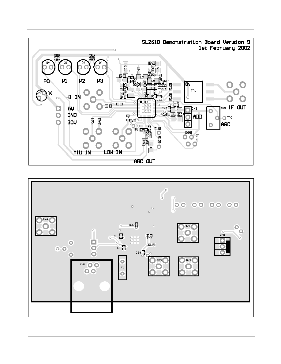
Figure 4 - SL2610 Evaluation Board Layout (Top)
Figure 5 - SL2610 Evaluation Board Layout (Bottom)

SL2610
Data Sheet
5
Zarlink Semiconductor Inc.
1.0 Functional Description
The SL2610 is a multi band RF mixer oscillator with image reject and on-board frequency synthesizer. It is intended
primarily for application in all band terrestrial tuners and requires a minimum external component count. It contains
all elements required for RF downconversion to a standard IF with the exception of external VCO tank circuits.
The pin allocation is contained in Figure 2 and the block diagram in Figure 1.
1.1 Mixer/oscillator section
In normal application the RF input is interfaced to the selected mixer oscillator preamplifier through the tuner
prefilter and AGC stages. The mixer input is arranged such that the signal can be coupled either differentially or
single-ended, and achieves the specified minimum performance in both configurations. Band input impedances
and NF are contained in Figure 11 and Figure 12 respectively. The converter two tone input spectra are contained
in Figure 13 and Figure 14.
The preamplifier output then feeds the mixer stage where the required channel is image reject downconverted to
the IF frequency. The local oscillator frequency for the downconversion is obtained from the on board local
oscillator, which uses an external varactor tuned tank. Typical VCO applications are contained in Figures 8, 9 and
10.
The output of the mixer is then fed to the converter output driver which presents a matched 200
differential load
to an external IF shaping filter.
The output of the shaping filter is then coupled into the IFAMP stage, which provides further gain and offers a 50
output impedance to interface direct with the tuner SAW filter.
The SL2610 contains a broadband level detect circuit whose output can be used to control the tuner AGC. The
target level of the AGC detector is controlled by the voltage applied to the AGCBIAS pin. The characteristic of the
target level is given in Figure 18.
1.2 PLL Frequency Synthesizer
The PLL frequency synthesizer section contains all the elements necessary, with the exception of a frequency
reference and loop filter, to control a varicap tuned local oscillator, so forming a complete PLL frequency
synthesised source. The device allows for operation with a high comparison frequency and is fabricated in high
speed logic, which enables the generation of a loop with good phase noise performance. It can also be operated
with comparison frequencies appropriate for frequency offsets as required in digital terrestrial (DTT) receivers.
The LO signal is multiplexed from the selected oscillator section to an internal preamplifier which provides gain and
reverse isolation from the divider signals. The output of the preamplifier interfaces direct with the 15-bit fully
programmable divider which is of MN+A architecture, where the dual modulus prescaler is 16/17, the A counter is
4-bits and the M counter is 11 bits.
The output of the programmable divider is fed to the phase comparator where it is compared in both phase and
frequency domain with the comparison frequency. This frequency is derived either from the on-board crystal
controlled oscillator or from an external reference source. In both cases the reference frequency is divided down to
the comparison frequency by the reference divider which is programmable into 1 of 29 ratios as detailed in Table 1.
The output of the phase detector feeds a charge pump and loop amplifier section which when used with an external
loop filter integrates the current pulses into the varactor line voltage.
The programmable divider output Fpd, divided by two and the reference divider output Fcomp, can be switched to
port P0 by programming the device into test mode. The test modes are described in Table 5.