 | –≠–ª–µ–∫—Ç—Ä–æ–Ω–Ω—ã–π –∫–æ–º–ø–æ–Ω–µ–Ω—Ç: SP5026DP | –°–∫–∞—á–∞—Ç—å:  PDF PDF  ZIP ZIP |
Document Outline
- Features
- Applications
- Description
- Figure 1 - Block Diagram
- Figure 2 - Pin Connections - Top View
- Functional Description
- Pin Compatibility
- Figure 3 - Data Format and Timing
- Figure 4 - Typical Application (FSTEP = 31.25kHz)
- Figure 5 - Typical Input Sensitivity
- Figure 6 - Input/Output Interface Circuits
- Figure 7 - Input/Output Interface Circuits
- Figure 8 - Typical Input Impedance
- Electrical Characteristics
- Electrical Characteristics Table�
- Absolute Maximum Ratings
- Absolute Maximum Ratings TableÅ �

Obsolescence Notice
This product is obsolete.
This information is available for your
convenience only.
For more information on
Zarlink's obsolete products and
replacement product lists, please visit
http://products.zarlink.com/obsolete_products/
1
Features
∑ Complete 1.OGHz Single Chip System
∑ Dual Standard 62.5kHz or 31.25 kHz Step Size
∑ Low power Consumption (5V 40mA)
∑ Function Compatible with Toshiba TD6380 and
TD6381*
∑ Pin Compatible with SP5510
∑ Low Radiation
∑ Varactor Drive Amplifier Disable
∑ Charge Pump Disable
∑ Single Port 18/19 Bit Serial Data Entry
∑ Four Controllable Outputs
∑ ESD Protection
See notes on pin compatibility
Normal ESD handling procedures should be observed
Applications
∑ Satellite TV when combined with SP4902 2.5GHz
Prescaler
∑ Cable tuning systems
∑ VCRs
Description
The SP5026 is a programming variant of the SP5510,
allowing the design of one tuner with either 1
2
C bus or
3-wire bus format depending on which device is
inserted. The SP5026, when used with a TV varicap
tuner, forms a complete phase locked loop tuning
system. The circuit consists of a divider-by-8 prescaler
with its own preamplifier and at 5-bit programmable
divider controlled by a serially-loaded data register.
Four open-collector outputs, each independently
programmable, are included. The device has two
modes of operation, selected by the "mode select"
input. In mode 1, the comparison frequency is
7.8125kHz and the programmable divider MSB is
bypassed; mode 2 comparison frequency is
3.90625kHz. The comparison frequencies are both
obtained from a 4MHz crystal controlled on-chip
oscillator.
DS5776
Issue 2
December 2002
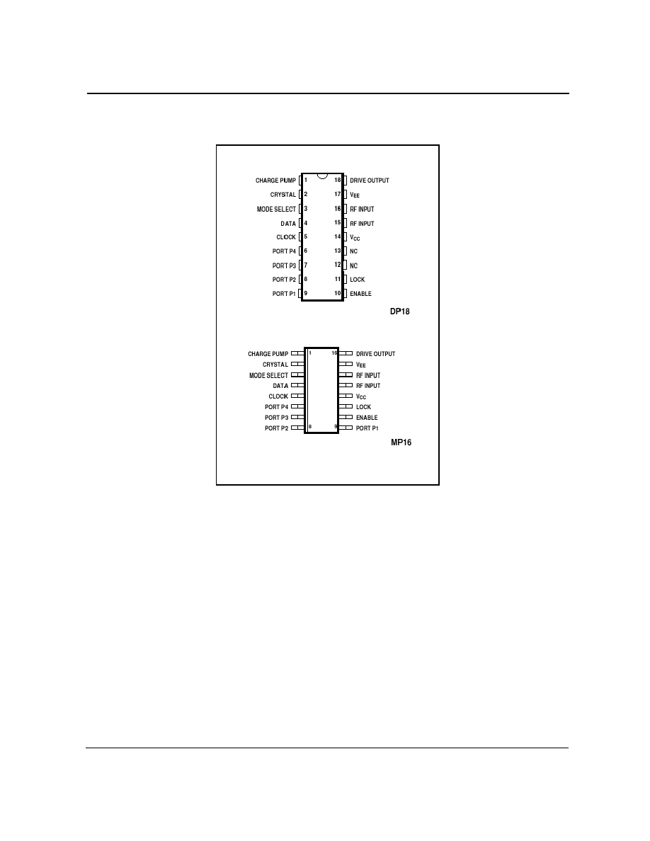
Ordering Information
SP5026 DP
18-lead plastic package)
SP5026S MP
(16-lead miniature plastic package)
SP5026
1.0GHz 3-Wire Bus Controlled Synthesizer
Data Sheet
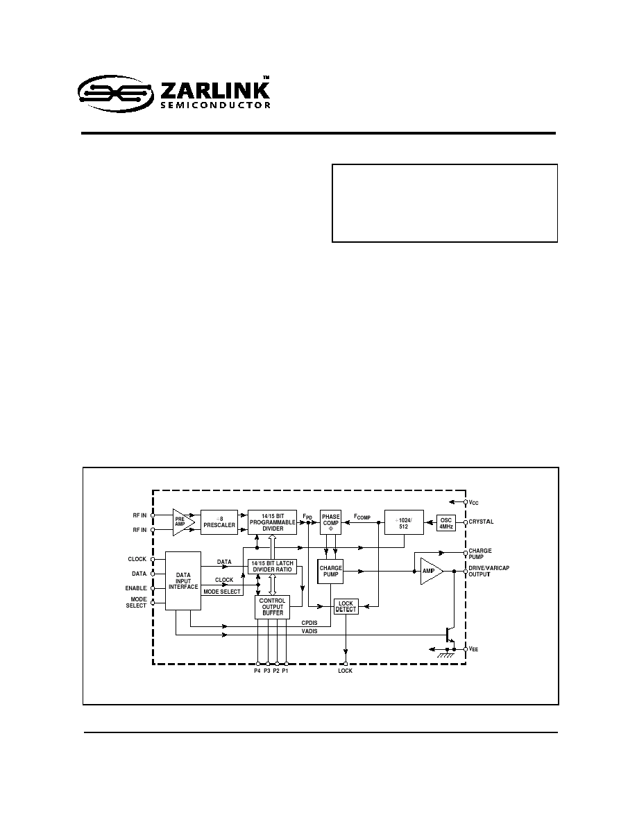
Figure 1 - Block Diagram
SP5026
Data Sheet
2
Zarlink Semiconductor Inc.
The comparator has a charge pump output with an amplifier stage around which feedback may be applied. Only
one external transistor is required for varicap line driving.
Figure 2 - Pin Connections - Top View
Functional Description
The SP5026 contains all the elements necessary, with the exception of reference crystal, loop filter and external
high voltage transistor to control a voltage controlled local oscillator, so forming a PLL frequency synthesized
source.
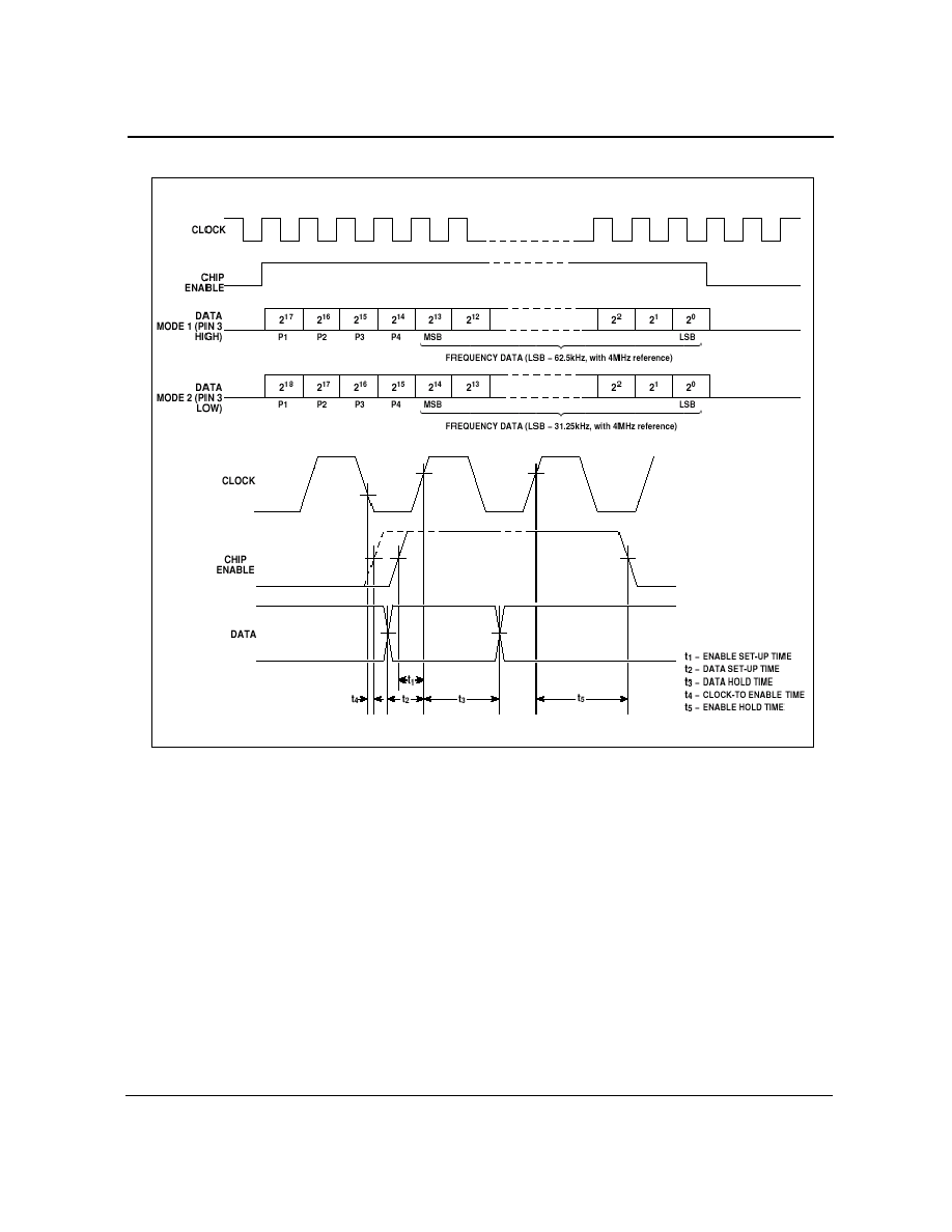
The system is controlled by a microprocessor via a standard data, clock enable three-wire bus. The data load
normally consists of a single word, which contains the frequency and port information and is only transferred to the
internal data shift register during an enable high period. The clock input is disabled during enable low periods.
New data words are only accepted by the internal data buffers from the shift register on a negative transition of the
enable, so giving improved fine tune facility for digital AFC etc.
The data sequence and timing follows the format shown in Figure 3.
The frequency is set by loading the programmable divider with the required 14/15 bit divisor word. The output of the
divider, F
PD
, is fed to the phase comparator where it is compared in phase and frequency domain to the internal
generated comparison frequency, F
COMP
.

Data Sheet
SP5026
3
Zarlink Semiconductor Inc.
The FC
COMP
is obtained by dividing the output of an on-chip crystal controlled oscillator. The crystal frequency used
is generally 4MHz, which gives an F
COMP
of 3.90625kHz/7.815kHz and, when multiplied back up to the synthesized
LO, gives a minimum step size of 31.25kHz/62.5kHz, respectively.
The programmable divider is preceded by an input RF preamplifier and high speed, low radiation prescaler. The
preamplifier is arranged to be self oscillating, so giving excellent input sensitivity. The input sensitivity and
impedance are shown in Figure 5 and Figure 7 respectively.
The SP5026 contains an improved lock detect circuit which generates a flag when the loop has attained lock. "Out
of Lock" is indicated by high impedance state.
The SP5026 contains 4 general purpose open collector outputs, ports P1-P4, which are capable of sinking at least
10mA. These outputs are set by the remaining four bits within the normal data word.
Pin Compatibility
The SP5026 may by used in SP5510 applications which require 3-wire bus as opposed to 1
2
C bus data format. In
SP5510 applications where the reference crystal is connected to pin 3, a small modification is required to ground
the crystal as shown in Figure 4.
Appropriate connections to the mode select input (pin 3) must also be made.
In mode 1 (pin 3 "HIGH") the SP5026 is programming and step size compatible with the Toshiba TD6380, and in
mode 2 (pin 3 "LOW") it is compatible with the TD6381.
SP5026
Data Sheet
4
Zarlink Semiconductor Inc.
Figure 3 - Data Format and Timing