
1
Zarlink Semiconductor Inc.
Zarlink, ZL and the Zarlink Semiconductor logo are trademarks of Zarlink Semiconductor Inc.
Copyright 2003, Zarlink Semiconductor Inc. All Rights Reserved.
Features
∑
3.45V Single Supply Operation
∑
Low Power Dissipation: 190mW typ
∑
Broadband: DC to 6GHz
∑
SSB Phase Noise (≠153dBc/Hz @ 10KHz)
∑
Pout 3dBm
Prescaler Modulus
∑
ZL40800 ≠ Divide by 8
∑
ZL40802 ≠ Divide by 16
Applications
∑
DC to 6 GHz PLL applications
∑
HyperLan
∑
LMDS
∑
Instrumentation
∑
Satellite Communications
∑
Fibre Optic Communications; OC48, OC192
∑
Ultra Low Jitter Clock Systems
Description
The ZL40800 and ZL40802 are Bipolar 3.45V supply,
very low power prescalers for professional applications
with a fixed modulus of 8 or 16. The ultra low close in
(1KHz offset) SSB phase noise performance is ideal for
narrow band communications systems or systems with
ultra low jitter budgets such as next generation fibre
optic communications. The devices are broadband from
DC to 6GHz.
See Figure 1 and Application Note for RF Prescalers for
more details.
July 2003
Ordering Information
ZL40800/DCA (tubes)
8 pin SOIC
ZL40800/DCB (tape and reel) 8 pin SOIC
ZL40802/DCA (tubes)
8 pin SOIC
ZL40802/DCB (tape and reel) 8 pin SOIC
-40
∞
C to 85
∞
C
ZL40800 and ZL40802
6 GHz Fixed Modulus Prescalers
˜
8 and
˜
16
Data Sheet
Figure 1 - Block Diagram
∑
Vref
Div N
10mA
200 Ohm
400 Ohm
VCC IN
VCC OUT
OUTPUT
OUTPUT B
INPUT
INPUT B
GND
GND
1
2
3
4
8
7
6
5

ZL40800 and ZL40802
Data Sheet
2
Zarlink Semiconductor Inc.
Figure 2 - Pin Connections - Top View
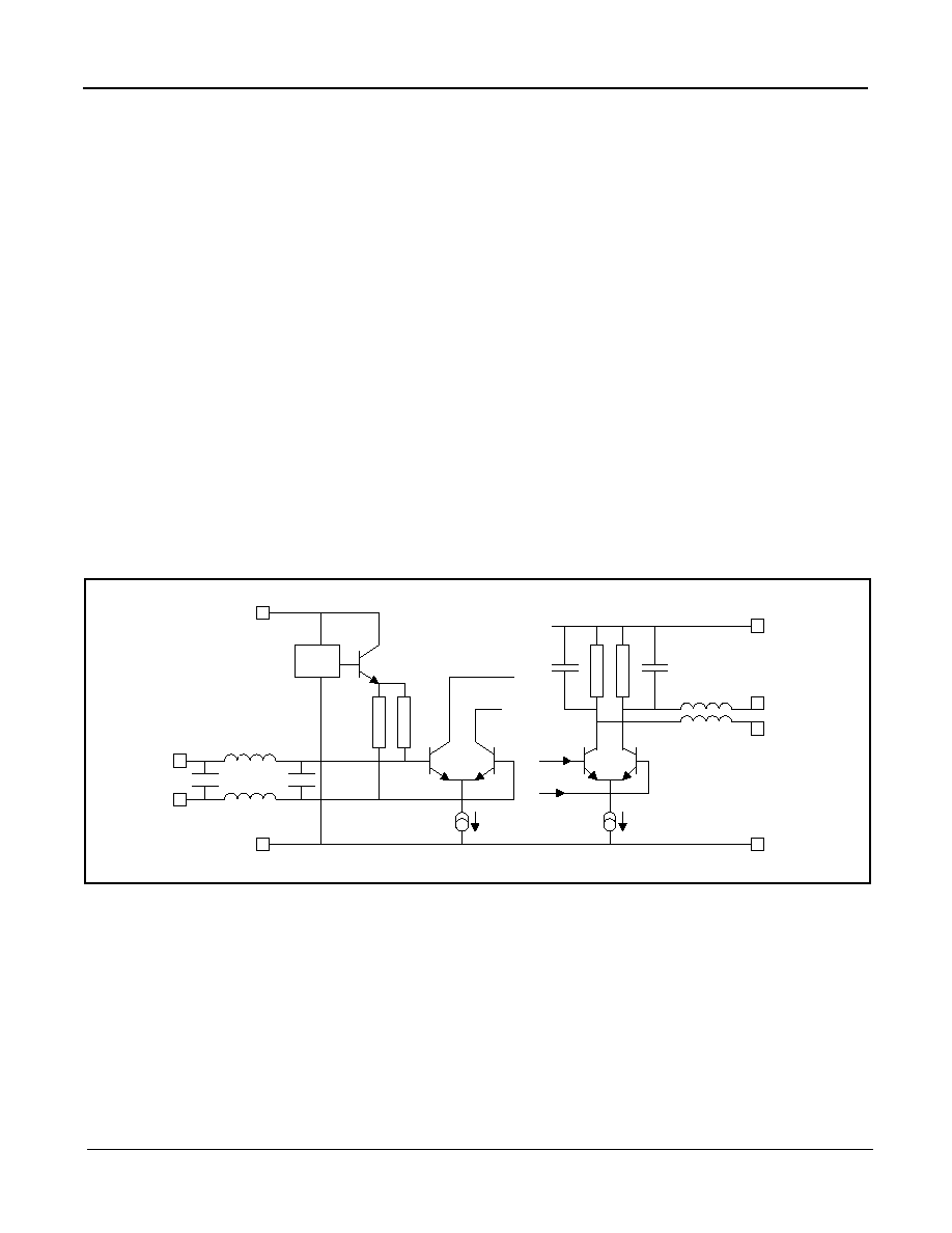
Application Configuration
Figure 3 shows a recommended application configuration. This example shows the device set up for single ended
operation.
Figure 3 - Recommended circuit configuration
This represents the circuit used to complete characterisation. The tabulated Electrical performance is guaranteed
using this application circuit.
Unpopulated evaluation boards are available, type No. ZLE40008. Fully populated evaluation boards are also
available, type Nos. ZLE40800 and ZLE40802.
1
2
3
4
8
7
6
5
Vcc IN
INPUT
INPUT Bar
GND
Vcc OUT
OUTPUT
OUTPUT Bar
GND
SOIC (N)
Application Diagram
C5: 10nF
C2: 10nF
C1: 1nF
C6: 10nF
1
2
3
4
8
7
6
5
C3: 100pF
C4: 100pF
Rsource:
Rload
R2
:
4
0
0
R
1
:
400
Rfilter
Note: Dotted Components Optional
ZL40800 and ZL40802
Data Sheet
3
Zarlink Semiconductor Inc.
Circuit Options
The application circuit includes some optional components that may be required to improve tolerance of system
noise present in the application.
Dummy R source may be added to the inverting input to provide a better matched source impedance at the input.
This will improve the rejection of common mode noise present within the system.
Dummy R load may be added to the inverting output to provide better matched load at the output. This will reduce
the radiated EMI at the output and reduce the Output Noise present on the supply rail.
R1 and R2 400 Ohm Pull ups are added to increase the headroom present at the amplifier output. This enhances
the operation at maximum supply and temperature. An alternative is to provide an inductive choke in place of R1
and R2.
These components provide a parallel DC Path to Vcc increasing the bandwidth of the output stage and providing a
virtually flat output power across frequency. See Fig 12 and 13.
Rfilter can be inserted between the Vcc in and the Vcc_out to provide additional filtering to the input Vcc. The input
Vcc powers the input bias reference only and can be a sensitive point to system noise. The nominal input current at
Vcc_IN s 0.35mA. An alternative would be to use an inductive choke.
C1 is additional Supply Filtering and should be added with Rfilter. The IC includes 10pF of on Chip Supply Filtering.
Input and Output Circuit
Figure 4 shows the equivalent input and output circuit.
Figure 4 - Input and Output Equivalent Circuit
I/O Circuits
20
0 O
h
m
20
0 O
h
m
10mA
0.5pF
1.0nH
1.0nH
0.5pF
Vcc_Out
Output
Output Bar
Gnd
Vref
Gnd
Input
Input bar
Vcc_In
1.0nH
1.0nH
0.2pF
400 O
h
m
400 O
h
m
0.8pF
∑
∑
∑
∑
∑
∑
∑
∑
∑
∑
∑
∑
∑ ∑
∑
∑
∑
∑

ZL40800 and ZL40802
Data Sheet
4
Zarlink Semiconductor Inc.
Increase Output Power Output Match and Narrow Band Operating Range
The device has been characterised with a mismatch at the output. This is a broadband configuration. 3dB more
output power is available if the application matches the load to the output impedance.
Figure 5 - ZL40802 Typical Phase Noise
Absolute Maximum Ratings
Parameter
Symbol
Min
Max
Units
1
Supply voltage
Vcc
-0.5
6
V
2
RFin
12
dBm
3
All I/O ports
-0.5
+0.5
V
4
ESD protection
2k
V
Mil-std 883B / 3015 cat1
5
Storage temperature
-55
+150
∞C
Operating Ranage
Parameter
Symbol
Min
Max
Units
1
Supply voltage
Vcc
3.3
3.6
V
2
RFin Frequency Range
0.1
6
GHz
3
Operating Junction Temperature
-40
125
∞C
4
Junc'n to Amb't resistance
Rth (j-a)
150
∞C/W
4 layer FR4 Board
5
Junc'n to Amb't resistance
Rth (j-c)
60
∞C/W
4 layer FR4 Board
ZL40802 Phase Noise vs Offset Freq
Pin = -6dBm, Vcc = 3.6V, Temp = 25C @ 1,3 & 5GHz
-160
-155
-150
-145
-140
-135
-130
100
1000
10000
100000
Offset Frequency in Hz
Ph
ase N
o
i
se i
n
d
B
C
/
H
z
5GHz
3GHz
1GHz

ZL40800 and ZL40802
Data Sheet
5
Zarlink Semiconductor Inc.
AC/DC Electrical Characteristics
These characteristics are guaranteed by design and characterisation over the following range of operating conditions unless otherwise stated:
Tamb = -40C to + 85C, Vcc = 3.3V to 3.6V.
Note 1:
Pin = power measured into 50 ohm Load from 50 Ohm Source.
Note 2:
Pout Single Ended AC coupled Single 50 Ohm Termination
Electrical Characteristics
Characteristic
Pin
Min.
Typ.
Max.
Units
Conditions
Icc_in (Supply current)
1
0.35
mA
ZL40800 Div8 & ZL40802 Div16
Icc_out (Supply current)
8
29
52
86
mA
ZL40800 Div8
Icc_out (Supply current)
8
31
55
89
mA
ZL40802 Div16
Input frequency
2,3
1
6
GHz
RMS sinewave,
Input sensitivity
2,3
-20
-10
dBm
fin = 1GHz to 6GHz, Note 1
Input overload
2,3
4
10
dBm
fin = 1GHz to 6GHz, Note 1
Phase Noise
6,7
-150
dBC/Hz
@ 1KHz Offset Fin = 3GHz
Output voltage
6,7
1
Vp-p
Differential Into 50ohm pull up
resistors
Output power
6,7
-7
-2
2
dBm
fin = 1GHz to 6GHz, Pin = -10dBm
Note 2
Output t-rise
6,7
110
ps
fin = 1GHz to 6GHz, Pin = -10dBm
Output t-fall
6,7
110
ps
fin = 1GHz to 6GHz, Pin = -10dBm
T ≠ prop delay
2,6
250
ps
50% IN to 50% OUT
Jitter
6,7
0.1
ps
Output Duty Cycle
6,7
45
50
55
%
fin = 1GHz to 6GHz, In = -10dBm
Input Edge Speed
2,3
500
V/us
For < 1GHz input operation

ZL40800 and ZL40802
Data Sheet
6
Zarlink Semiconductor Inc.
Figure 6 - Typical Input Sensitivity (sine wave drive)
Figure 7 - Single Ended AC Coupled Single Termination
Typical Input Sensitivity (Sinewave Drive)
-35
-30
-25
-20
-15
-10
-5
0
5
10
15
0
1
2
3
4
5
6
7
8
9
Input Frequency (GHz)
V
i
n into 50 O
h
m
(dB
m
)
Guaranteed Operating Range
-40C to 85C
Edge
Speed
>500V/us
Single Ended AC Coupled Single Termination
( + 400 Ohm or Choke Pull Up )
Vcc out
Gnd
20
0 Ohm
20
0 Ohm
50
O
h
m
40
0 Ohm
Transmission Line
Pre-scaler Output
400
Oh
m
50 Ohm
Optional
Balance
ZL40800 and ZL40802
Data Sheet
7
Zarlink Semiconductor Inc.
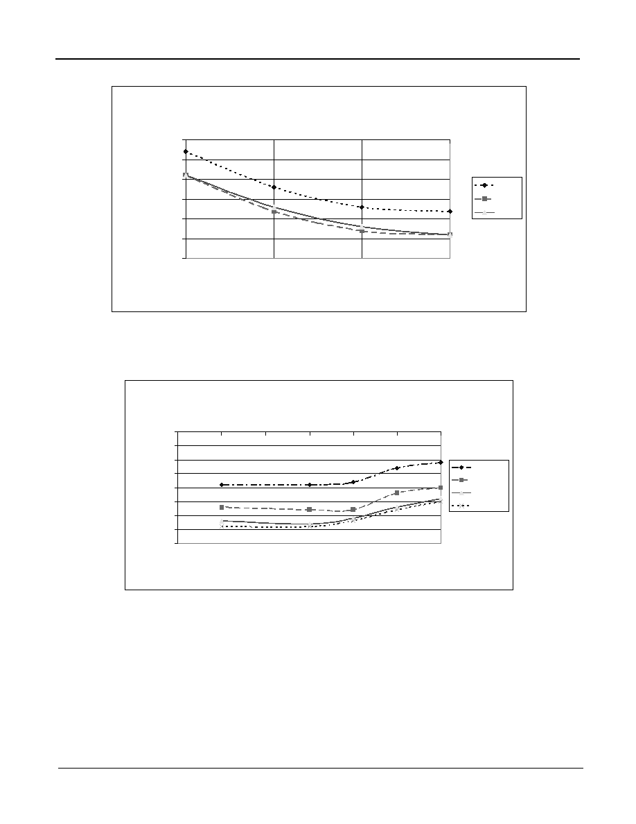
Figure 8 - ZL40800 Typical Phase Noise
Figure 9 - ZL40800 Phase Noise vs Input Frequency
ZL40800 Phase Noise vs Offset
Pin = 2dBm, Vcc = 3.6V, Temp = 25C
-160
-155
-150
-145
-140
-135
-130
100
1000
10000
100000
Offset frequency in Hz
P
h
aase N
o
ise in
d
BC/
Hz
5GHz
3GHz
1GHz
ZL40800: Phase Noise vs Input Frequency
@ 2.5dBm Pin, 3.6V Supply, 25C
-160
-155
-150
-145
-140
-135
-130
-125
-120
0
1
2
3
4
5
6
Input Frequency (GHz)
P
h
ase N
o
ise (dB
c/H
z
)
100 Hz
1 KHz
10 KHz
100 KHz
ZL40800 and ZL40802
Data Sheet
8
Zarlink Semiconductor Inc.
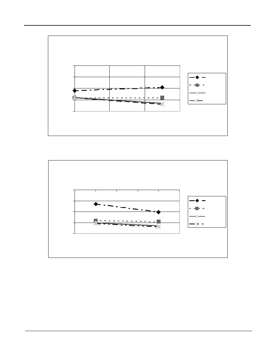
Figure 10 - ZL40800 Phase Noise vs Input Power
Figure 11 - ZL40800 Phase Noise vs Vcc
ZL40800: Phase Noise v Pin,
3.6V Supply, Fin = 3GHz, T = 25C
-160
-150
-140
-130
-120
-10
-5
0
5
Pin (dBm)
Ph
ase N
o
i
se (d
B
c
/
H
z
)
100 Hz
1 KHz
10 KHz
100 KHz
ZL40800: Phase Noise v Vcc
Fin = 3GHz, Pin = -6dBm, T =25C
-160
-150
-140
-130
-120
3.2
3.3
3.4
3.5
3.6
3.7
Supply Voltage (V)
Ph
ase N
o
i
se (d
B
c
/
H
z
)
100 Hz
1 KHz
10 KHz
100 KHz

ZL40800 and ZL40802
Data Sheet
9
Zarlink Semiconductor Inc.
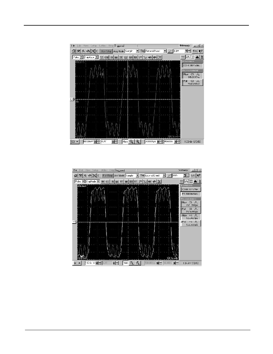
Single Ended or Differential Load
Figure 12 and Figure 13 illustrate the output waveform when measured differential and single ended with a 6GHz
waveform at the input at a level of +2dBm. The single ended output contains some input frequency breakthrough
which contributes to the distortion present. This is a common mode signal which is rejected if the output is taken
differentially.
Differential operation also provides an additional 3dB. Differential Operation reduces the radiated EMI in the system
and reduces the susceptibility to common mode system noise.
Figure 12 - ZL40800 Pout / Input Frequency
Figure 13 - ZL40800Pout v Input Frequency
(Vcc=3.3V, T= -40C,25C, 85C)
ZL40800_Dev1 (/8) with 400R pull-ups
Frequency_sweep, Vcc = 3.6v
-6
-5
-4
-3
-2
-1
0
1
0
1E+09
2E+09
3E+09
4E+09
5E+09
6E+09
7E+09
8E+09
i/p frequency (Hz)
o/
p l
e
v
e
l
(
d
B
m
)
Device 1,Temperature = 25∞C
Device 1,Temperature = 85∞C
ZL40802_dev1_Frequency_sweep, Vcc = 3.3v
-8
-7
-6
-5
-4
-3
-2
-1
0
1000000000
10000000000
i/p frequency (Hz)
o/
p l
e
v
e
l
(
d
B
m
)
Device 1,Temperature = -40∞C
Device 1,Temperature = 25∞C
Device 1,Temperature = 85∞C
ZL40800 and ZL40802
Data Sheet
10
Zarlink Semiconductor Inc.
Figure 14 - ZL40800 Single Ended Out @ 5Ghz +2dBm
Figure 15 - ZL40800 Differential Out @ 5Ghz +2dBm


www.zarlink.com
Information relating to products and services furnished herein by Zarlink Semiconductor Inc. trading as Zarlink Semiconductor or its subsidiaries (collectively
"Zarlink") is believed to be reliable. However, Zarlink assumes no liability for errors that may appear in this publication, or for liability otherwise arising from the
application or use of any such information, product or service or for any infringement of patents or other intellectual property rights owned by third parties which may
result from such application or use. Neither the supply of such information or purchase of product or service conveys any license, either express or implied, under
patents or other intellectual property rights owned by Zarlink or licensed from third parties by Zarlink, whatsoever. Purchasers of products are also hereby notified
that the use of product in certain ways or in combination with Zarlink, or non-Zarlink furnished goods or services may infringe patents or other intellectual property
rights owned by Zarlink.
This publication is issued to provide information only and (unless agreed by Zarlink in writing) may not be used, applied or reproduced for any purpose nor form part
of any order or contract nor to be regarded as a representation relating to the products or services concerned. The products, their specifications, services and other
information appearing in this publication are subject to change by Zarlink without notice. No warranty or guarantee express or implied is made regarding the
capability, performance or suitability of any product or service. Information concerning possible methods of use is provided as a guide only and does not constitute
any guarantee that such methods of use will be satisfactory in a specific piece of equipment. It is the user's responsibility to fully determine the performance and
suitability of any equipment using such information and to ensure that any publication or data used is up to date and has not been superseded. Manufacturing does
not necessarily include testing of all functions or parameters. These products are not suitable for use in any medical products whose failure to perform may result in
significant injury or death to the user. All products and materials are sold and services provided subject to Zarlink's conditions of sale which are available on request.
Purchase of Zarlink's I
2
C components conveys a licence under the Philips I
2
C Patent rights to use these components in an I
2
C System, provided that the system
conforms to the I
2
C Standard Specification as defined by Philips.
Zarlink, ZL and the Zarlink Semiconductor logo are trademarks of Zarlink Semiconductor Inc.
Copyright 2003, Zarlink Semiconductor Inc. All Rights Reserved.
TECHNICAL DOCUMENTATION - NOT FOR RESALE
For more information about all Zarlink products
visit our Web Site at