SUMMARY
NPN Transistor
V
CEO
= 20V; R
SAT
= 47m ;
C
= 4.5A
Schottky Diode
V
R
= 40V; V
F
= 500mV (@1A); I
C
=1A
DESCRIPTION
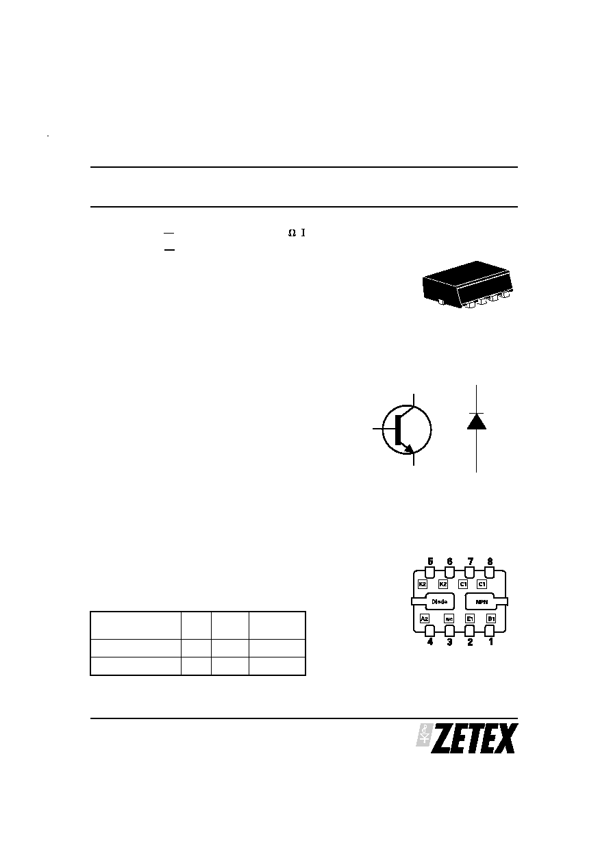
Packaged in the new innovative 3mm x 2mm MLP this combination dual
comprises an ultra low saturation PNP transistor and a 1A Schottky barrier
diode. This excellent combination provides users with highly efficient
performance in applications including DC-DC and charging circuits.
Users will also gain several other key benefits:
Performance capability equivalent to much larger packages
Improved circuit efficiency & power levels
PCB area and device placement savings
Lower package height (0.9mm nom)
Reduced component count
FEATURES
∑
Extremely Low Saturation Voltage (150mV @1A)
∑
H
FE
characterised up to 6A
∑
I
C
= 4.5A Continuous Collector Current
∑
Extremely Low V
F
, fast switching Schottky
∑
3mm x 2mm MLP
APPLICATIONS
∑
DC - DC Converters
∑
Mobile Phones
∑
Charging Circuits
∑
Motor control
DEVICE MARKING
BS1
ZX3CDBS1M832
ISSUE 1 - JUNE 2002
MPPSTM Miniature Package Power Solutions
20V NPN LOW SATURATION TRANSISTOR AND 40V, 1A SCHOTTKY
DIODE COMBINATION DUAL
1
Cathode
Anode
B
C
E
DEVICE
REEL
TAPE
WIDTH
QUANTITY
PER REEL
ZX3CDBS1M832TA
7
8mm
3000
ZX3CDBS1M832TC
13
8mm
10000
ORDERING INFORMATION
3mm x 2mm Dual Die MLP
3mm x 2mm Dual MLP
underside view
PINOUT

ZX3CDBS1M832
ISSUE 1 - JUNE 2002
2
PARAMETER
SYMBOL
VALUE
UNIT
Transistor
Collector-Base Voltage
V
CBO
40
V
Collector-Emitter Voltage
V
CEO
20
V
Emitter-Base Voltage
V
EBO
7.5
V
Peak Pulse Current
I
CM
12
A
Continuous Collector Current (a)(f)
I
C
4.5
A
Continuous Collector Current (b)(f)
I
C
5
A
Base Current
I
B
1000
mA
Power Dissipation at TA=25∞C (a)(f)
Linear Derating Factor
P
D
1.5
12
W
mW/∞C
Power Dissipation at TA=25∞C (b)(f)
Linear Derating Factor
P
D
2.45
19.6
W
mW/∞C
Power Dissipation at TA=25∞C (c)(f)
Linear Derating Factor
P
D
1
8
W
mW/∞C
Power Dissipation at TA=25∞C (d)(f)
Linear Derating Factor
P
D
1.13
9
W
mW/∞C
Power Dissipation at TA=25∞C (d)(g)
Linear Derating Factor
P
D
1.7
13.6
W
mW/∞C
Power Dissipation at TA=25∞C (e)(g)
Linear Derating Factor
P
D
3
24
W
mW/∞C
Storage Temperature Range
T
stg
-55 to +150
∞C
Junction Temperature
T
j
150
∞C
ABSOLUTE MAXIMUM RATINGS.
PARAMETER
SYMBOL
VALUE
UNIT
Junction to Ambient (a)(f)
R
JA
83
∞C/W
Junction to Ambient (b)(f)
R
JA
51
∞C/W
Junction to Ambient (c)(f)
R
JA
125
∞C/W
Junction to Ambient (d)(f)
R
JA
111
∞C/W
Junction to Ambient (d)(g)
R
JA
73.5
∞C/W
Junction to Ambient (e)(g)
R
JA
41.7
∞C/W
THERMAL RESISTANCE
Notes
(a) For a dual device surface mounted on 8 sq cm single sided 2oz copper on FR4 PCB, in still air conditions with all exposed pads attached. The
copper area is split down the centre line into two separate areas with one half connected to each half of the dual device.
(b) Measured at t<5 secs for a dual device surface mounted on 8 sq cm single sided 2oz copper on FR4 PCB, in still air conditions with all exposed
pads attached. The copper area is split down the centre line into two separate areas with one half connected to each half of the dual device.
(c) For a dual device surface mounted on 8 sq cm single sided 2oz copper on FR4 PCB, in still air conditions with minimal lead connections only.
(d) For a dual device surface mounted on 10 sq cm single sided 1oz copper on FR4 PCB, in still air conditions with all exposed pads attached
attached. The copper area is split down the centre line into two separate areas with one half connected to each half of the dual device.
(e) For a dual device surface mounted on 85 sq cm single sided 2oz copper on FR4 PCB, in still air conditions with all exposed pads attached
attached. The copper area is split down the centre line into two separate areas with one half connected to each half of the dual device.
(f) For a dual device with one active die.
(g) For dual device with 2 active die running at equal power.
(h) Repetitive rating - pulse width limited by max junction temperature. Refer to Transient Thermal Impedance graph.
(i) The minimum copper dimensions required for mounting are no smaller than the exposed metal pads on the base of the device as shown in the
package dimensions data. The thermal resistance for a dual device mounted on 1.5mm thick FR4 board using minimum copper 1 oz weight, 1mm
wide tracks and one half of the device active is Rth = 250∞C/W giving a power rating of Ptot = 500mW.
ZX3CDBS1M832
ISSUE 1 - JUNE 2002
3
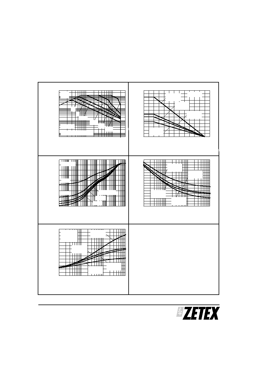
0.1
1
10
0.01
0.1
1
10
0
25
50
75
100
125
150
0.0
0.5
1.0
1.5
2.0
2.5
3.0
3.5
100µ
1m
10m 100m
1
10
100
1k
0
20
40
60
80
0.1
1
10
100
0
25
50
75
100
125
150
175
200
225
0.1
1
10
100
0.0
0.5
1.0
1.5
2.0
2.5
3.0
3.5
Note (a)(f)
100us
100ms
1s
V
CE(SAT)
Limited
1ms
Safe Operating Area
Single Pulse, T
amb
=25∞C
DC
10ms
I
C
Co
l
l
e
c
t
o
r
Cu
r
r
e
n
t
(
A
)
V
CE
Collector-Emitter Voltage (V)
1oz Cu
Note (d)(f)
1oz Cu
Note (d)(g)
2oz Cu
Note (a)(f)
2oz Cu
Note (e)(g)
Derating Curve
T
amb
=25∞C
M
a
x
Pow
e
r
D
i
s
s
i
pa
t
i
on
(
W
)
Temperature (∞C)
Note (a)(f)
D=0.2
D=0.5
D=0.1
Transient Thermal Impedance
Single Pulse
D=0.05
T
h
e
r
m
a
l
R
e
si
st
a
n
ce
(
∞
C
/
W
)
Pulse Width (s)
1oz copper
Note (g)
1oz copper
Note (f)
2oz copper
Note (f)
2oz copper
Note (g)
Thermal Resistance v Board Area
T
h
e
r
m
a
l
R
e
si
st
a
n
ce
(
∞
C
/
W
)
Board Cu Area (sqcm)
1oz copper
Note (g)
2oz copper
Note (g)
1oz copper
Note (f)
2oz copper
Note (f)
Power Dissipation v Board Area
T
amb
=25∞C
T
j max
=150∞C
Continuous
P
D
D
i
s
s
i
pa
t
i
on
(
W
)
Board Cu Area (sqcm)
TRANSISTOR TYPICAL CHARACTERISTICS
ZX3CDBS1M832
ISSUE 1 - JUNE 2002
4
PARAMETER
SYMBOL
VALUE
UNIT
Schottky Diode
Continuous Reverse Voltage
V
R
40
V
Forward Voltage @ I
F
=1000mA(typ)
V
F
425
A
Forward Current
I
F
1850
mA
Average Peak Forward Current D=50%
I
FAV
3
A
Non Repetitive Forward Current t
100 s
t
10ms
I
FSM
12
7
A
A
Power Dissipation at TA=25∞C (a)(f)
Linear Derating Factor
P
D
1.2
12
W
mW/∞C
Power Dissipation at TA=25∞C (b)(f)
Linear Derating Factor
P
D
2
20
W
mW/∞C
Power Dissipation at TA=25∞C (c)(f)
Linear Derating Factor
P
D
0.8
8
W
mW/∞C
Power Dissipation at TA=25∞C (d)(f)
Linear Derating Factor
P
D
0.9
9
W
mW/∞C
Power Dissipation at TA=25∞C (d)(g)
Linear Derating Factor
P
D
1.36
13.6
W
mW/∞C
Power Dissipation at TA=25∞C (e)(g)
Linear Derating Factor
P
D
2.4
24
W
mW/∞C
Storage Temperature Range
T
stg
-55 to +150
∞C
Junction Temperature
T
j
125
∞C
ABSOLUTE MAXIMUM RATINGS.
PARAMETER
SYMBOL
VALUE
UNIT
Junction to Ambient (a)(f)
R
JA
83
∞C/W
Junction to Ambient (b)(f)
R
JA
51
∞C/W
Junction to Ambient (c)(f)
R
JA
125
∞C/W
Junction to Ambient (d)(f)
R
JA
111
∞C/W
Junction to Ambient (d)(g)
R
JA
73.5
∞C/W
Junction to Ambient (e)(g)
R
JA
41.7
∞C/W
THERMAL RESISTANCE
Notes
(a) For a dual device surface mounted on 8 sq cm single sided 2oz copper on FR4 PCB, in still air conditions with all exposed pads attached. The
copper area is split down the centre line into two separate areas with one half connected to each half of the dual device.
(b) Measured at t<5 secs for a dual device surface mounted on 8 sq cm single sided 2oz copper on FR4 PCB, in still air conditions with all exposed
pads attached. The copper area is split down the centre line into two separate areas with one half connected to each half of the dual device.
(c) For a dual device surface mounted on 8 sq cm single sided 2oz copper on FR4 PCB, in still air conditions with minimal lead connections only.
(d) For a dual device surface mounted on 10 sq cm single sided 1oz copper on FR4 PCB, in still air conditions with all exposed pads attached
attached. The copper area is split down the centre line into two separate areas with one half connected to each half of the dual device.
(e) For a dual device surface mounted on 85 sq cm single sided 2oz copper on FR4 PCB, in still air conditions with all exposed pads attached
attached. The copper area is split down the centre line into two separate areas with one half connected to each half of the dual device.
(f) For a dual device with one active die.
(g) For dual device with 2 active die running at equal power.
(h) Repetitive rating - pulse width limited by max junction temperature. Refer to Transient Thermal Impedance graph.
(i) The minimum copper dimensions required for mounting are no smaller than the exposed metal pads on the base of the device as shown in the
package dimensions data. The thermal resistance for a dual device mounted on 1.5mm thick FR4 board using minimum copper 1 oz weight, 1mm
wide tracks and one half of the device active is Rth = 250∞C/W giving a power rating of Ptot = 400mW.
ZX3CDBS1M832
ISSUE 1 - JUNE 2002
5
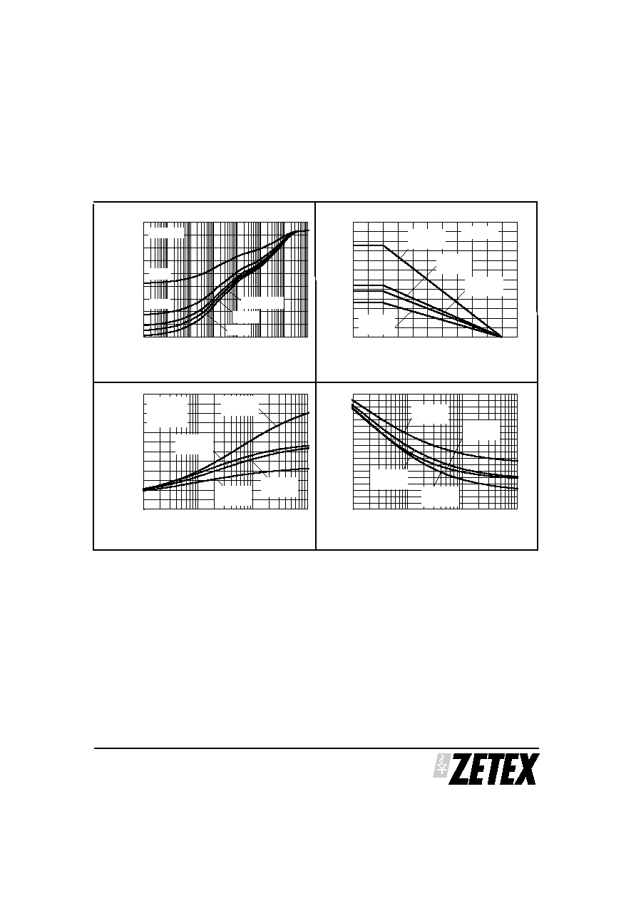
0
25
50
75
100
125
0.0
0.5
1.0
1.5
2.0
2.5
3.0
100µ
1m
10m 100m
1
10
100
1k
0
20
40
60
80
0.1
1
10
100
0
25
50
75
100
125
150
175
200
225
0.1
1
10
100
0.0
0.5
1.0
1.5
2.0
2.5
3.0
1oz Cu
Note (d)(f)
1oz Cu
Note (d)(g)
2oz Cu
Note (a)(f)
2oz Cu
Note (e)(g)
Derating Curve
T
amb
=25∞C
M
a
x
Pow
e
r
D
i
s
s
i
pa
t
i
on
(
W
)
Temperature (∞C)
Note (a)(f)
D=0.2
D=0.5
D=0.1
Transient Thermal Impedance
Single Pulse
D=0.05
T
h
e
r
m
a
l
R
e
si
st
a
n
ce
(
∞
C
/
W
)
Pulse Width (s)
1oz copper
Note (g)
1oz copper
Note (f)
2oz copper
Note (f)
2oz copper
Note (g)
Thermal Resistance v Board Area
T
h
e
r
m
a
l
R
e
si
st
a
n
ce
(
∞
C
/
W
)
Board Cu Area (sqcm)
1oz copper
Note (g)
2oz copper
Note (g)
1oz copper
Note (f)
2oz copper
Note (f)
Power Dissipation v Board Area
T
amb
=25∞C
T
j max
=125∞C
Continuous
P
D
D
i
s
s
i
pa
t
i
on
(
W
)
Board Cu Area (sqcm)
SCHOTTKY TYPICAL CHARACTERISTICS