S E M I C O N D U C T O R S
SUMMARY
BV
CEO
= -30V : R
SAT
= 24m ; I
C
= -5.5A
DESCRIPTION
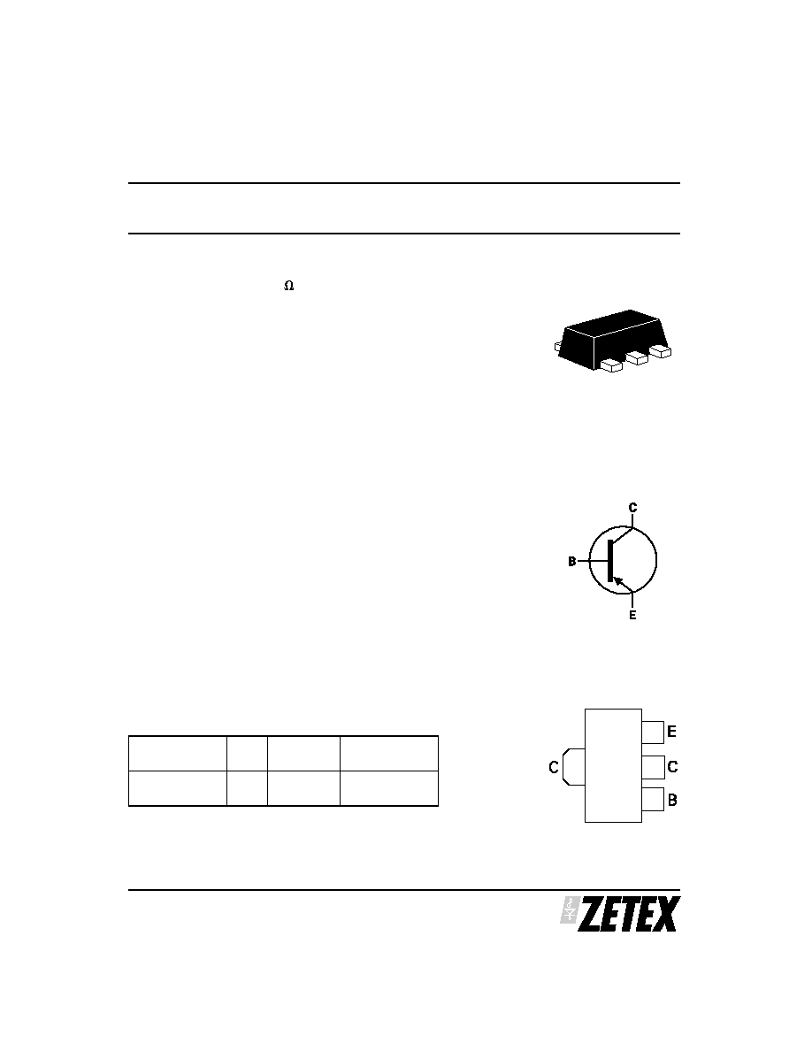
Packaged in the SOT89 outline this new 5th generation
low saturation 30V PNP transistor offers low on state
losses making it ideal for use in DC-DC circuits, line
switching and various driving and power management
functions.
FEATURES
∑
5.5 Amps continuous current
∑
Up to 20 Amps peak current
∑
Very low saturation voltages
∑
Exceptional gain linearity down to 10mA
∑
Excellent high current gain hold up
APPLICATIONS
∑
DC - DC converters
∑
MOSFET gate drivers
∑
Charging circuits
∑
Power switches
∑
Motor control
DEVICE MARKING
∑
949
ZX5T949Z
ISSUE 3 - DECEMBER 2004
MPPSTM 30V PNP LOW SATURATION MEDIUM POWER TRANSISTOR
IN SOT89
1
SOT89
PINOUT
TOP VIEW
DEVICE
REEL
SIZE
TAPE WIDTH
QUANTITY PER
REEL
ZX5T949ZTA
7"
12mm
embossed
1000 units
ORDERING INFORMATION
ZX5T949Z
S E M I C O N D U C T O R S
ISSUE 3 - DECEMBER 2004
2
PARAMETER
SYMBOL
LIMIT
UNIT
Collector-base voltage
BV
CBO
-50
V
Collector-emitter voltage
BV
CEO
-30
V
Emitter-base voltage
BV
EBO
-7
V
Continuous collector current
(a)
I
C
-5.5
A
Peak pulse current
I
CM
-20
A
Power dissipation at T
A
=25∞C
(a)
Linear derating factor
P
D
1.5
12
W
mW/∞C
Power dissipation at T
A
=25∞C
(b)
Linear derating factor
P
D
2.1
16.8
W
mW/∞C
ABSOLUTE MAXIMUM RATINGS
PARAMETER
SYMBOL
VALUE
UNIT
Junction to Ambient
(a)
R
JA
83
∞C/W
Junction to Ambient
(b)
R
JA
60
∞C/W
NOTES
(a) For a device surface mounted on 25mm x 25mm x 1.6mm FR4 PCB with high coverage of single sided 1oz copper, in still air conditions.
(b) For a device surface mounted on 50mm x 50mm x 1.6mm FR4 PCB with high coverage of single sided 1oz copper, in still air conditions.
THERMAL RESISTANCE
ZX5T949Z
S E M I C O N D U C T O R S
ISSUE 3 - DECEMBER 2004
3
CHARACTERISTICS

ZX5T949Z
S E M I C O N D U C T O R S
ISSUE 3 - DECEMBER 2004
4
PARAMETER
SYMBOL
MIN.
TYP.
MAX.
UNIT
CONDITIONS
Collector-base breakdown voltage
BV
CBO
-50
-70
V
I
C
= -100 A
Collector-emitter breakdown voltage BV
CER
-50
-70
V
I
C
= -1 A, RB <1k
Collector-emitter breakdown voltage BV
CEO
-30
-40
V
I
C
= -10mA *
Emitter-base breakdown voltage
BV
EBO
-7.0
-8.0
V
I
E
= -100 A
Collector cut-off current
I
CBO
<-1
-20
-0.5
nA
A
V
CB
= -40V
V
CB
= -40V,T
amb
=100∞C
Collector cut-off current
I
CER
R <1k
<-1
-20
-0.5
nA
A
V
CB
= -40V
V
CB
= -40V,T
amb
=100∞C
Emitter cut-off current
I
EBO
<-1
-10
nA
V
EB
= -6V
Collector-emitter saturation voltage
V
CE(SAT)
-25
-35
-55
-55
-130
-40
-55
-80
-80
-175
mV
mV
mV
mV
mV
I
C
= -0.5A, I
B
= -20mA *
I
C
= -1A, I
B
= -100mA *
I
C
= -1A, I
B
= -20mA *
I
C
= -2A, I
B
= -200mA *
I
C
= -5.5A, I
B
=-500mA *
Base-emitter saturation voltage
V
BE(SAT)
-970
-1070
mV
I
C
= -5.5A, I
B
= -500mA *
Base-emitter turn-on voltage
V
BE(ON)
-860
-960
mV
I
C
= -5.5A, V
CE
= -1V *
Static forward current transfer ratio
h
FE
100
100
70
10
225
200
145
20
300
I
C
= -10mA, V
CE
= -1V *
I
C
= -1A, V
CE
= -1V *
I
C
= -5A, V
CE
= -1V *
I
C
= -20A, V
CE
= -1V *
Transition frequency
f
T
110
MHz
I
C
= -100mA, V
CE
= -10V
f = 50MHz
Output capacitance
C
OBO
83
pF
V
CB
= -10V, f = 1MHz *
Switching times
t
ON
t
OFF
43
230
ns
I
C
= -1A, V
CC
= -10V,
I
B1
= -I
B2
= -100mA
ELECTRICAL CHARACTERISTICS (at T
amb
= 25∞C unless otherwise stated)
NOTES
* Measured under pulsed conditions. Pulse width
300 s; duty cycle
2%.

ZX5T949Z
S E M I C O N D U C T O R S
ISSUE 3 - DECEMBER 2004
5
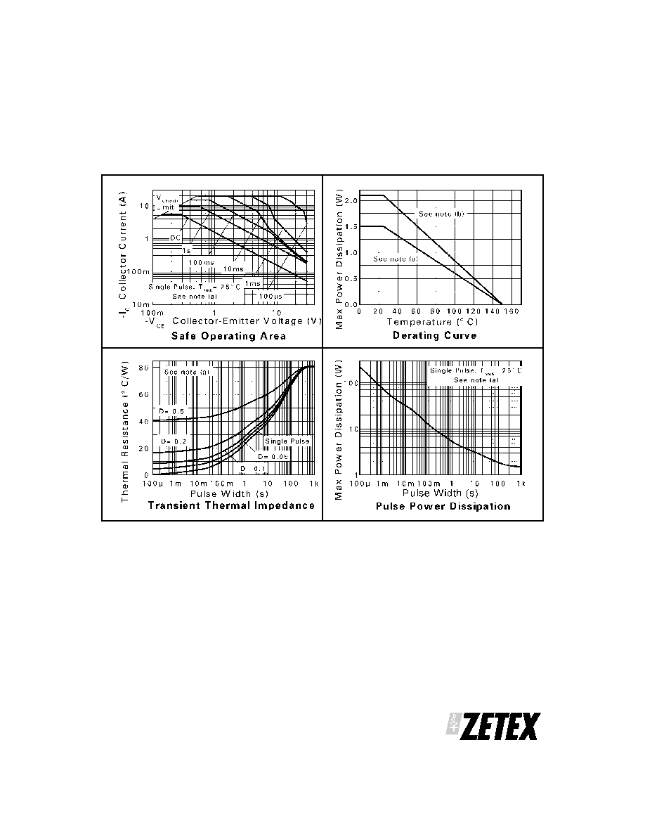
TYPICAL CHARACTERISTICS
ZX5T949Z
S E M I C O N D U C T O R S
6
ISSUE 3 - DECEMBER 2004
Europe
Zetex GmbH
Streitfeldstraþe 19
D-81673 M¸nchen
Germany
Telefon: (49) 89 45 49 49 0
Fax: (49) 89 45 49 49 49
europe.sales@zetex.com
Americas
Zetex Inc
700 Veterans Memorial Hwy
Hauppauge, NY 11788
USA
Telephone: (1) 631 360 2222
Fax: (1) 631 360 8222
usa.sales@zetex.com
Asia Pacific
Zetex (Asia) Ltd
3701-04 Metroplaza Tower 1
Hing Fong Road, Kwai Fong
Hong Kong
Telephone: (852) 26100 611
Fax: (852) 24250 494
asia.sales@zetex.com
Corporate Headquaters
Zetex Semiconductors plc
Lansdowne Road, Chadderton
Oldham, OL9 8NP
United Kingdom
Telephone (44) 161 622 4444
Fax: (44) 161 622 4446
hq@zetex.com
These offices are supported by agents and distributors in major countries world-wide.
This publication is issued to provide outline information only which (unless agreed by the Company in writing) may not be used, applied or reproduced
for any purpose or form part of any order or contract or be regarded as a representation relating to the products or services concerned. The Company
reserves the right to alter without notice the specification, design, price or conditions of supply of any product or service.
For the latest product information, log on to
www.zetex.com
© Zetex Semiconductors plc 2004
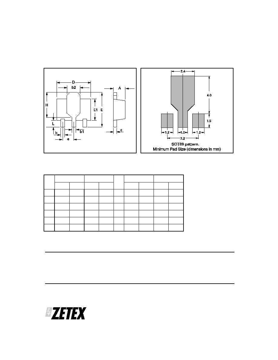
Controlling dimensions are in millimeters. Approximate conversions are given in inches
PACKAGE OUTLINE
PAD LAYOUT DETAILS
DIM
Millimeters
Inches
DIM
Millimeters
Inches
Min
Max
Min
Max
Min
Max
Min
Max
A
1.40
1.60
0.550
0.630
e
1.40
1.50
0.055
0.059
b
0.38
0.48
0.015
0.019
E
3.75
4.25
0.150
0.167
b1
-
0.53
-
0.021
E1
-
2.60
-
0.102
b2
1.50
1.80
0.060
0.071
G
2.90
3.00
0.114
0.118
c
0.28
0.44
0.011
0.017
H
2.60
2.85
0.102
0.112
D
4.40
4.60
0.173
0.181
-
-
-
-
-
PACKAGE DIMENSIONS