 | –≠–ª–µ–∫—Ç—Ä–æ–Ω–Ω—ã–π –∫–æ–º–ø–æ–Ω–µ–Ω—Ç: ZX5T951Z | –°–∫–∞—á–∞—Ç—å:  PDF PDF  ZIP ZIP |

1
S E M I C O N D U C T O R S
SUMMARY
BV
CEO
= -60V : R
SAT
= 32m ; I
C
= -4.3A
DESCRIPTION
Packaged in the SOT89 outline this new 5
th
generation low saturation 60V PNP
transistor offers low on state losses making it ideal for use in DC-DC circuits, line
switching and various driving and power management functions.
FEATURES
∑
Extremely low equivalent on-resistance; R
SAT
= 32mV at 5A
∑
4.3 amps continuous current
∑
Up to 15 amps peak current
∑
Very low saturation voltages
∑
Excellent gain characteristics specified up to 10 amps
APPLICATIONS
∑
Emergency lighting circuits
∑
Motor driving (including DC fans)
∑
Solenoid, relay and actuator drivers
∑
DC-DC modules
∑
Backlight inverters
∑
Power switches
∑
MOSFET gate drivers
DEVICE MARKING
∑
951
ZX5T951Z
ISSUE 2 - DECEMBER 2004
60V PNP LOW SATURATION MEDIUM POWER TRANSISTOR IN SOT89
DEVICE
REEL
SIZE
TAPE
WIDTH
QUANTITY PER
REEL
ZX5T951ZTA
7"
12mm
embossed
1000 units
ORDERING INFORMATION
PINOUT
TOP VIEW
SOT89
ZX5T951Z
S E M I C O N D U C T O R S
ISSUE 2 - DECEMBER 2004
2
PARAMETER
SYMBOL
VALUE
UNIT
Junction to ambient
(a)
R
JA
83
∞C/W
Junction to ambient
(b)
R
JA
60
∞C/W
NOTES
(a) For a device surface mounted on 25mm x 25mm x 1.6mm FR4 PCB with high coverage of single sided 1oz copper, in still air conditions.
(b) For a device surface mounted on 50mm x 50mm x 1.6mm FR4 PCB with high coverage of single sided 1oz copper, in still air conditions.
THERMAL RESISTANCE
PARAMETER
SYMBOL
LIMIT
UNIT
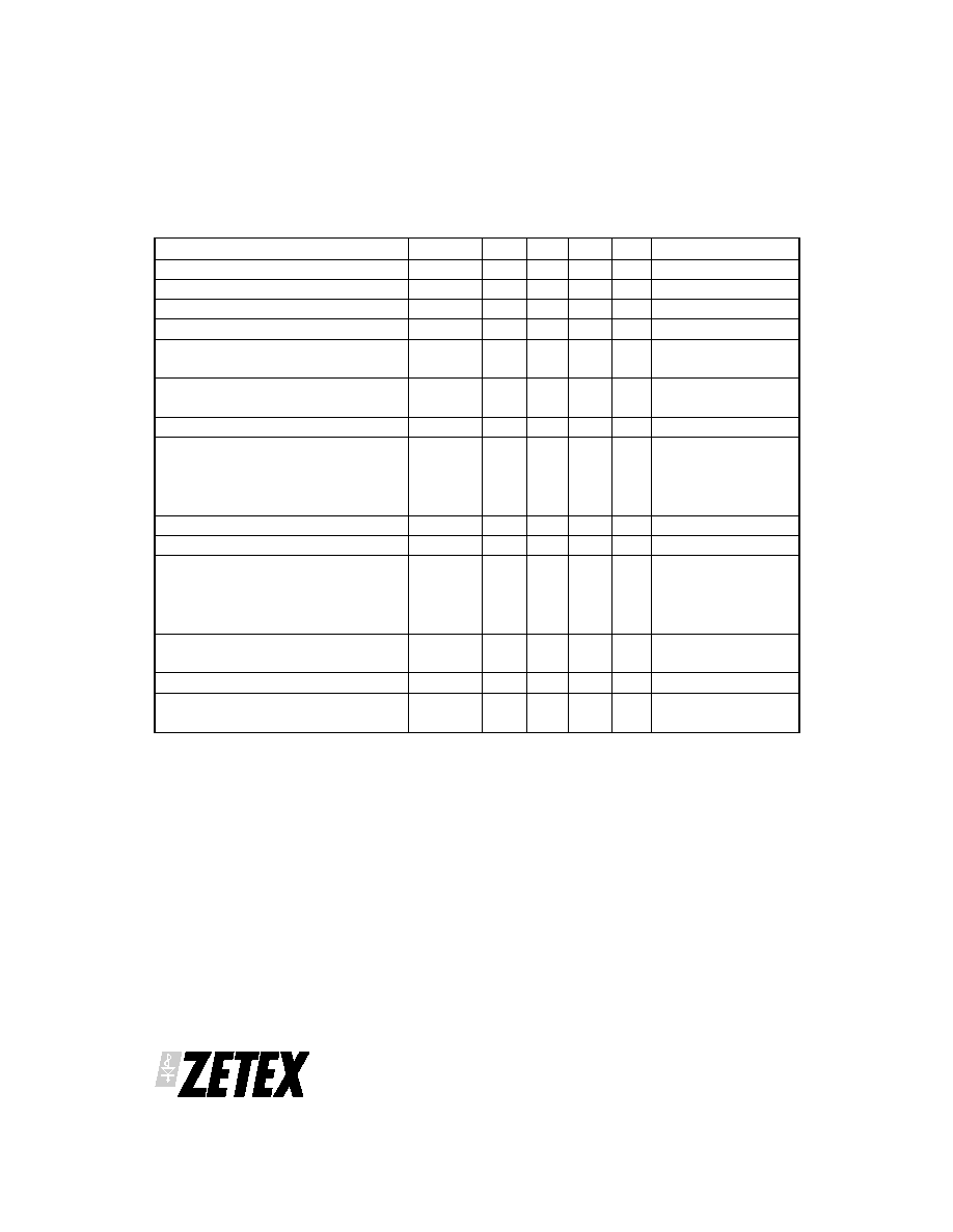
Collector-base voltage
BV
CBO
-100
V
Collector-emitter voltage
BV
CEO
-60
V
Emitter-base voltage
BV
EBO
-7
V
Continuous collector current
(a)
I
C
-4.3
A
Peak pulse current
I
CM
-15
A
Power dissipation at T
A
=25∞C
(a)
Linear derating factor
P
D
1.5
12
W
mW/∞C
Power dissipation at T
A
=25∞C
(b)
Linear derating factor
P
D
2.1
16.8
W
mW/∞C
Operating and storage temperature range
T
j
, T
stg
-55 to +150
∞C
ABSOLUTE MAXIMUM RATINGS

ZX5T951Z
S E M I C O N D U C T O R S
ISSUE 2 - DECEMBER 2004
3
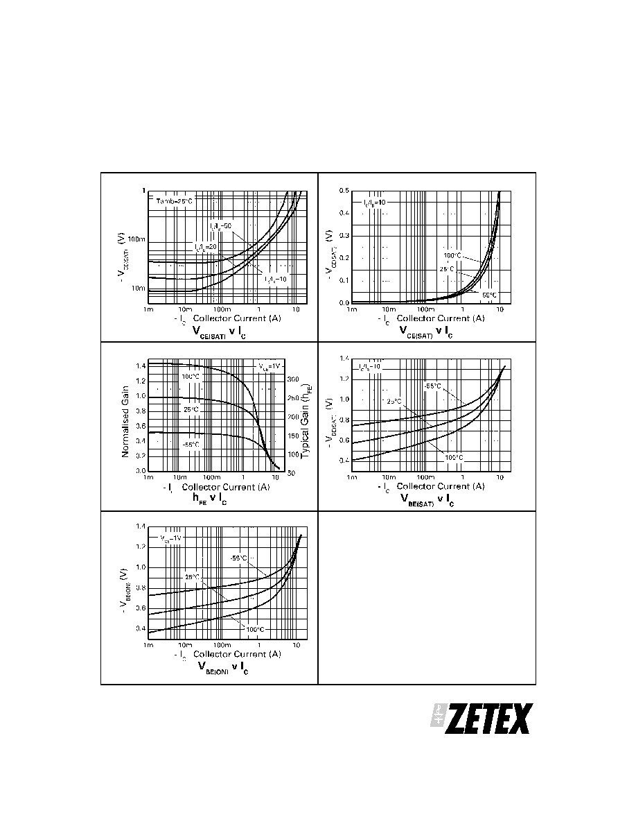
CHARACTERISTICS
ZX5T951Z
S E M I C O N D U C T O R S
ISSUE 2 - DECEMBER 2004
4
PARAMETER
SYMBOL
MIN.
TYP.
MAX.
UNIT CONDITIONS
Collector-base breakdown voltage
BV
CBO
-100
-120
V
I
C
=-100 A
Collector-emitter breakdown voltage
BV
CER
-100
-120
V
I
C
=-1 A, RB
1k
Collector-emitter breakdown voltage
BV
CEO
-60
-80
V
I
C
=-10mA*
Emitter-base breakdown voltage
BV
EBO
-7
-8.1
V
I
E
=-100 A
Collector cut-off current
I
CBO
1
-20
-0.5
nA
A
V
CB
=-80V
V
CB
=-80V,T
amb
=100 C
Collector cut-off current
I
CER
R
1k
1
-20
-0.5
nA
A
V
CB
=-80V
V
CB
=-80V,T
amb
=100 C
Emitter cut-off current
I
EBO
1
-10
nA
V
EB
=-6V
Collector-emitter saturation voltage
V
CE(SAT)
-14
-50
-75
-160
-20
-65
-110
-215
mV
mV
mV
mV
I
C
=-0.1A, I
B
=-10mA*
I
C
=-1A, I
B
=-100mA*
I
C
=-2A, I
B
=-200mA*
I
C
=-5A, I
B
=-500mA*
Base-emitter saturation voltage
V
BE(SAT)
-950
-1050
mV
I
C
=-5A, I
B
=-500mA*
Base-emitter turn-on voltage
V
BE(ON)
-840
-950
mV
I
C
=-5A, V
CE
=-1V*
Static forward current transfer ratio
H
FE
100
100
45
10
250
200
90
25
300
I
C
=-10mA, V
CE
=-1V*
I
C
=-2A, V
CE
=-1V*
I
C
=-5A, V
CE
=-1V*
I
C
=-10A, V
CE
=-1V*
Transition frequency
f
T
120
MHz I
C
=-100mA, V
CE
=-10V
f=50MHz
Output capacitance
C
OBO
48
pF
V
CB
=-10V, f=1MHz*
Switching times
t
ON
t
OFF
39
370
ns
I
C
=-1A, V
CC
=-10V,
I
B1
=I
B2
=-100mA
ELECTRICAL CHARACTERISTICS (at T
amb
= 25∞C unless otherwise stated)
* Measured under pulsed conditions. Pulse width
300 s; duty cycle
2%.
ZX5T951Z
S E M I C O N D U C T O R S
ISSUE 2 - DECEMBER 2004
5
TYPICAL CHARACTERISTICS