DEVICE DESCRIPTION
The ZXCP330 is the first in a series of switched capacitor DC to DC converters,
converting an input voltage from between 2 volts and 4.4 volts to a regulated
output voltage of 3.3V with a maximum load current of 40mA. The device
operates with one flying capacitor and two small bypass capacitors at input
and output making for a very small solution. Very low quiescent current
makes these devices ideal for low power and battery powered applications.
Regulation is achieved by sensing the output and enabling the device charge pump when it falls below the sense
threshold. This technique leads to high efficiency conversion. The method is also efficient for low current loads.
Here the duty cycle will be low and the quiescent current drawn whilst the charge pump is disabled is very small.
The device includes a pin for logic controlled shutdown of the output, and also features thermal shutdown, which
protects against short circuit damage as well as excessive temperatures. The device is supplied in a 6 lead SOT-23
package.
Contact Zetex marketing for availability of other voltage options.
FEATURES
∑
Very low power: I
Q
= 20µA
∑
Regulated output voltage: 3.3V, ± 4%
∑
Output current: 20mA at V
IN
= 2V
∑
Output current: 40mA at V
IN
= 2.5V
∑
No inductors required
∑
Very low shutdown current: <1µA
∑
Short circuit and over-temp protected
∑
Very small package: SOT23-6 pin
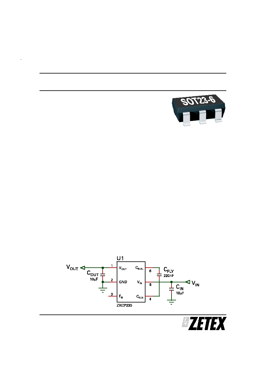
APPLICATIONS DIAGRAM
APPLICATIONS
∑
Battery backup supplies
∑
Smart card readers
∑
Li-Ion battery backup supplies
∑
SIM interface supplies for cellular phones
∑
Hand held computers
ZXCP330
PROVISIONAL ISSUE A - DECEMBER 2001
1
SWITCHED CAPACITOR DC-DC CONVERTER
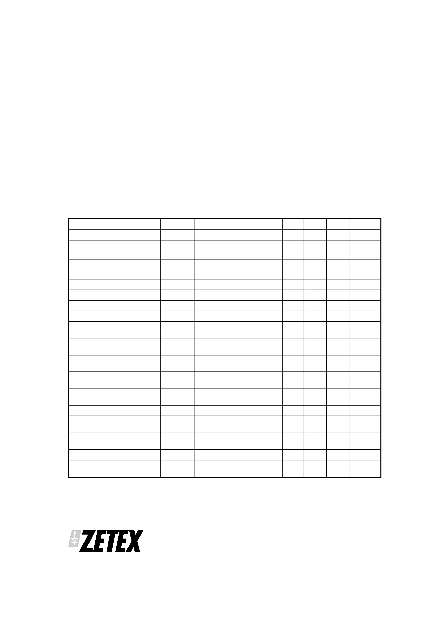
ABSOLUTE MAXIMUM RATINGS
V
IN
to G
ND
-0.3V to +7V
E
N
to ground
-0.3V to +7V
V
OUT
to ground
-0.3V to +5.5V
I
OUT
150mA
Operating Temperature
-40∞C to 85∞C
Storage Temperature Range
-55∞C to 125∞C
Continuous Power Dissipation
Thermally ltd
ZXCP330
PROVISIONAL ISSUE A - DECEMBER 2001
2
PARAMETER
SYMBOL
CONDITIONS
MIN
TYP
MAX
UNIT
Input Voltage
V
IN
2.0
4.4
V
Output Voltage
Note 1
V
OUT
2V
V
IN
4.4V, I
OUT
20mA
2.5V
V
IN
4.4V, I
OUT
40mA
3.17
3.17
3.3
3.3
3.43
3.43
V
Maximum Output Current
I
O(max)
V
IN
2V
V
IN
2.5V
20
40
mA
Output Short-Circuit Current
I
SC
V
IN
= 2V
125
mA
Supply Current
I
Q
2V
V
IN
4.4V , No load
20
40
A
Efficiency
V
IN
=2V, I
OUT
= 20mA
82
%
Switching Frequency
f
OSC
Oscillator free running
500
kHz
Line Regulation (Note 2)
V
LDR
V
IN
=2.5V to 4.4V, I
OUT
=40mA,
T
A
=25∞C
-50
0
50
mV
Load Regulation (Note 2)
V
LDR
I
OUT
=1mA to 40mA, V
IN
=2.5V
T
A
=25∞C
-50
0
50
mV
Output Voltage Ripple
V
R
f=500kHz, V
IN
=2.5V,
I
OUT
= 40mA
20
mV pk-pk
Enable pin Input Threshold
High
V
EN(ON)
Device active
1.5
5.5
V
Enable pin Input Threshold
Low
V
EN(OFF
)
Device shutdown
0
0.3
V
Enable pin Input current
I
EN
T
A
=25∞C, E
N
= 4.4V
100
nA
Shutdown supply Current
I
Q(SD)
E
N
=0V, 2V
V
IN
4.4V,
T
A
=25∞C
1
A
Shutdown time (Note 3)
T
SD
V
IN
= 2.5V, E
N
changes from
1.5V to 0.3V
20
s
V
OUT
Turn-on Time
T
ON
V
IN
=2V, I
OUT
= 0mA
500
s
Thermal Shutdown
Temperature
T
SD
135
150
165
∞C
ELECTRICAL CHARACTERISTICS
TEST CONDITIONS (unless otherwise stated): T
A
=-40∞C to 85∞C, (typical values at 25∞), E
N
= V
IN
, C
FLY
=0.22 F,
C
IN
=10 F, C
OUT
=10 F
Note 1: Contact Zetex marketing for availability of alternative output voltages
Note 2: Output can deviate EITHER side of Vnominal for increased load current or line voltage
Note 3: Shutdown time is the time taken for I
IN
to reduce to <1 A

Operational description
The ZXCP330 uses a standard switched capacitor
voltage doubler topology to generate a regulated
output of 3.3V from an input voltage of between 2V and
4.4V. A 500kHz internal clock generates two phases.
During
1 (Phi One) the flying capacitor is connected
between Vin and ground for 1 s. During 2 the bottom
plate is connected to V
IN
and the top plate connected to
V
OUT
. A proportion of the output voltage is compared
with a silicon band gap to maintain regulation. This is
achieved by disabling the switching operation when
the output voltage is above 3.3V and re-enabling when
the output voltage falls below 3.3V. When the input
voltage is near the higher limit, a large amount of
charge is acquired by the flying capacitor during
1,
which would result in excessive output ripple. For this
reason, the 2 phase is cut short if the voltage exceeds
3.3V, so that the full charge on the flying capacitor is
not delivered to the output capacitor, hence ripple is
reduced
.
When the charge pump is disabled, the current drawn
by the switches themselves is <1 A. This means that at
zero loads, the load on the output will only consist of
the divider driving the output comparator and the band
gap circuit, resulting the device cycling very slowly and
drawing only 20 A.
When the circuit is either waiting for the next cycle or
when it is shutdown by taking the ENABLE pin low, it
remains in the 1 state so that the flying capacitor stays
charged to the input voltage ready for 2 to be enabled
immediately. During shutdown all analogue circuits
are switched off, resulting in a current drain of <100nA.
Power efficiency
The ZXCP330 is essentially a regulated voltage
doubling charge pump. As for all voltage doubling
charge pumps the input current is always twice the
output current. The efficiency equation for an ideal
voltage doubler is given below:
=
=
◊
◊
=
P
P
V
I
2I
V
V
2V
OUT
IN
OUT
OUT
OUT
IN
OUT
IN
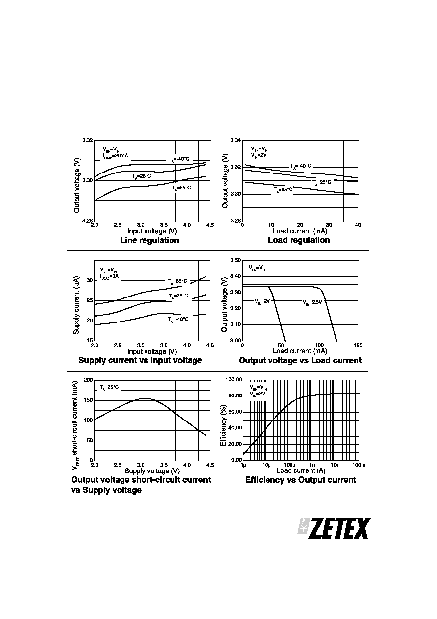
The ZXCP330 maintains good efficiency at light loads
because of its inherently low power design. At higher
loads switching losses are minimal so efficiency is
close to the ideal. See Efficiency vs Output current
graph in the typical characteristics section.
Short circuit/thermal protection
When the output of the ZXCP330 is short circuited, the
resultant current depends on 2 factors. At low input
voltages, the internal resistance of the switches limits
the current and so it will increase with input voltage.
However since, under this condition, all the input
power is dissipated in the chip, it will self-heat. When
the input voltage reaches around 3.2V, the value
depending on the thermal mounting of the device, the
chip temperature reaches a nominal value of 150 C and
a thermal shutdown circuit inhibits the switching. The
device will then cool and the thermal shutdown will
re-enable the switching.
It will cycle in and out of
operation indefinitely until the short circuit is removed.
Since the thermal shutdown circuit is then maintaining
constant die temperature, it becomes a "constant
power sink", so an increase in the input voltage results
in the on time becoming proportionately less so the
current decreases to maintain constant power.
Capacitor selection
Output capacitors are a critical choice in the overall
performance of the solution. Output voltage ripple,
converter output power and turn-on time are
influenced by the choice of capacitor. To reduce noise
and output voltage ripple multi layer ceramic
capacitors are recommended for use at the ZXCP330
input and output because of their inherently low ESR,
typically <0.1 .
The ZXCP330 will function satisfactorily over a wide
range of capacitor values and load currents. However,
to achieve maximum output current and minimum
output ripple it is important to choose the values
carefully. Available output current increases with the
value of the flying capacitor, with input voltage and
with clock frequency (which is fixed internally). Ripple
increases with input voltage and the ratio of the flying
capacitor to the output capacitor.
ZXCP330
PROVISIONAL ISSUE A - DECEMBER 2001
5
Block Diagram