1
ISSUE 4 - DECEMBER 2001
ZXCT1010
DESCRIPTION
The ZXCT1010 is a high side current sense monitor.
Using this device eliminates the need to disrupt the
ground plane when sensing a load current.
It is an enhanced version of the ZXCT1009 offering
reduced typical output offset and improved accuracy
at low sense voltage.
The wide input voltage range of 20V down to as low as
2.5V make it suitable for a range of applications. A
minimum operating current of just 4µA, combined
with its SOT23-5 package make suitable for portable
battery equipment.
FEATURES
∑
Low cost, accurate high-side current sensing.
∑
Output voltage scaling.
∑
Up to 2.5V sense voltage.
∑
2.5V ≠ 20V supply range.
∑
300nA typical offset current.
∑
4µA quiescent current.
∑
1% typical accuracy.
∑
SOT23 -5 package.
APPLICATIONS
∑
Battery Chargers
∑
Smart Battery Packs
∑
DC Motor control
∑
Over current monitor
∑
Power Management
∑
Level translating
∑
Programmable current source
ENHANCED HIGH-SIDE CURRENT MONITOR
APPLICATION CIRCUIT
ORDERING INFORMATION
PART NUMBER
PACKAGE
PARTMARKING
ZXCT1010E5
SOT23-5
1010
V
V
I
in
in
out
To Load
V
out
R
sense
R
out
Load
GND
ZXCT1010

2
ISSUE 4 - DECEMBER 2001
ZXCT1010
ABSOLUTE MAXIMUM RATINGS
Voltage on any pin
-0.6V to 20V (relative to GND)
Continuous output current
25mA
Continuous sense voltage
V
in
+ 0.5V > V
sense
> V
in
≠ 5V
Operating Temperature
-40 to 85
∞
C
Storage Temperature
-55 to 125
∞
C
Package Power Dissipation
(T
A
= 25
∞
C)
SOT23-5
500mW
ELECTRICAL CHARACTERISTICS
Test Conditions T
A
= 25
∞
C, V
in
= 5V, R
out
= 100
.
SYMBOL
PARAMETER
CONDITIONS
LIMITS
UNIT
Min
Typ
Max
V
in
V
CC
Range
2.5
20
V
I
out
1
Output current
V
sense
= 0V
V
sense
= 10mV
V
sense
= 100mV
V
sense
= 200mV
V
sense
= 1V
0
85
0.975
1.95
9.7
0.3
100
1.00
2.00
10.0
10
115
1.025
2.05
10.3
µA
µA
mA
mA
mA
I
q
Ground pin current
V
sense
= 0V
1
4
8
µA
V
sense
2
Sense Voltage
0
2500
mV
I
sense
Load pin
input current
100
nA
Acc
Accuracy
R
sense
= 0.1
V
sense
= 200mV
-2.5
2.5
%
Gm
Transconductance,
I
out
/ V
sense
10000
µA/V
BW
Bandwidth
RF P
in
= -20dBm
3
V
sense
= 10mV dc
V
sense
= 100mV dc
300
2
kHz
MHz
1
Includes input offset voltage contribution
2
V
sense
=V
in
-V
load
3
-20dBm=63mVp-p into 50

4
ISSUE 4 - DECEMBER 2001
ZXCT1010
PIN DESCRIPTION
Pin Name
Pin Function
V
in
Supply Voltage
Load
Connection to load/battery
I
out
Output current, proportional to V
in
-V
load
GND
Ground
SOT23-5
Package Suffix ≠ E5
Top View
CONNECTION DIAGRAM
+
-
V
in
Load
I
out
100
SCHEMATIC DIAGRAM
1
2
3
4
5
NC
GND
I
out
Load
V
IN

ISSUE 4 - DECEMBER 2001
ZXCT1010
5
The following lines describe how to scale a load
current to an output voltage.
V
sense
= V
in
- V
load
V
out
= 0.01 x V
sense
x R
out
1
E.g.
A 1A current is to be represented by a 100mV output
voltage:
1)Choose the value of R
sense
to give 50mV > V
sense
>
500mV at full load.
For example V
sense
= 100mV at 1.0A. R
sense
= 0.1/1.0
=> 0.1 ohms.
2)Choose R
out
to give V
out
= 100mV, when V
sense
=
100mV.
Rearranging
1
for R
out
gives:
R
out
= V
out
/(V
sense
x 0.01)
R
out
= 0.1 / (0.1 x 0.01) = 100
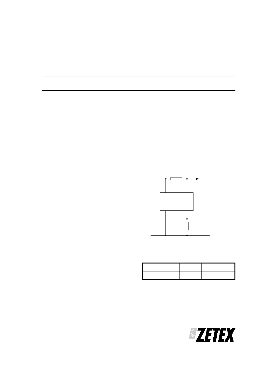
TYPICAL CIRCUIT APPLICATION
POWER DISSIPATION
The maximum allowable power dissipation of the
device for normal operation (Pmax), is a function of
the package junction to ambient thermal resistance
(
ja), maximum junction temperature (Tjmax), and
ambient temperature (Tamb), according to the
expression:
P
max
= (Tj
max
≠ T
amb
) /
ja
The device power dissipation, P
D
is given by the
expression:
P
D
=I
out
.(V
in
-V
out
) Watts
Where R
load
represents any load including DC motors,
a charging battery or further circuitry that requires
monitoring, R
sense
can be selected on specific
requirements of accuracy, size and power rating.
APPLICATIONS INFORMATION
V
V
I
in
in
out
V
out
R
sense
R
out
R
load
Load
GND
ZXCT1010
