 | –≠–ª–µ–∫—Ç—Ä–æ–Ω–Ω—ã–π –∫–æ–º–ø–æ–Ω–µ–Ω—Ç: ZXCT1051 | –°–∫–∞—á–∞—Ç—å:  PDF PDF  ZIP ZIP |
Issue 1 - January 2006
1
www.zetex.com
© Zetex Semiconductors plc 2006
ZXCT1051
Precision wide input range current monitor
Description
The ZXCT1051 is a wide input range current
monitor, which operates over a range of input
voltages from ground up to V
CC
-2V. As a result
the ZXCT1051 can be used on the high or low
side of the load.
The very low offset voltage enables a typical
accuracy of 1% for sense voltages of only
30mV, giving better tolerances for small sense
resistors necessary at higher currents.
Features
∑
Accurate down to end current sensing
∑
Output voltage scaling x10
∑
0 to V
CC
-2V sense input range
∑
2.7 to 20V supply range
∑
50 µA quiescent current
∑
1% typical accuracy
∑
SOT23-5 package
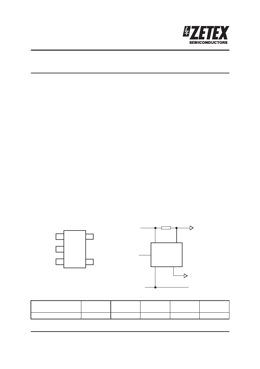
Pin connections
The ZXCT1051 provides a fixed gain of 10
thereby removing the need for an additional
resistor.
Applications
∑
Power supply
∑
DC motor and solenoid control
∑
Battery management
∑
Over current monitor
∑
Power management
∑
Short circuit detection
Typical application circuit
Ordering information
V
CC
GND
V
OUT
V
SENSE
-
V
SENSE
+
ZXCT1051
V
SENSE
+
V
CC
GND
V
OUT
V
OUT
V
SENSE
-
V
SENSE
-
V
SENSE
+
R
SENSE
Order code
Package
Partmark
Reel size
(inches)
Tape width
(mm)
Quantity
per reel
ZXCT1051E5TA
SOT23-5
1051
7
8
3,000
ZXCT1051
Issue 1 - January 2006
2
www.zetex.com
© Zetex Semiconductors plc 2006
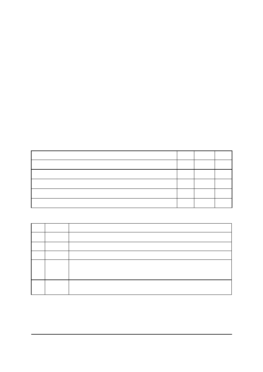
Absolute maximum ratings
V
CC
max.
20V
Voltage on V
SENSE
- and V
SENSE
+
-0.6 to V
CC
Voltage on all other pins
-0.6V and V
CC
+0.6V
V
SENSE
"(V
SENSE
+) - (V
SENSE
-)
500 mV
Operating temperature, T
A
-40 to 125∞C
Storage temperature
-55 to 150∞C
Maximum junction temperature
150∞C
Package power dissipation
300mW at T
A
= 25∞C (de-rate to zero at 150∞C)
Operation above the absolute maximum rating may cause device failure. Operation at the
absolute maximum ratings, for extended periods, may reduce device reliability.
Recommended operating conditions
Pin function table
Parameter
Min.
Max.
Units
V
SENSE+
Common-mode sense input range
0
V
CC
-2
V
V
CC
Supply voltage range
2.7
20
V
V
SENSE
Differential sense input voltage range
0
0.3
V
V
OUT
Output voltage range
0
V
CC
- 2
V
T
A
Ambient temperature range
-40
125
∞C
PIN
Name
Description
1
V
CC
This is the analog supply and provides power to internal circuitry
2
GND
Ground pin
3
OUT
Output voltage pin. NMOS source follower with 20µA bias to ground
4
V
SENSE
+
This is the positive input of the current monitor and has an input range from
0V up to V
CC
≠ 2V. The current through this pin varies with differential sense
voltage
5
V
SENSE
-
This is the negative input of the current monitor and has an input range
from 0V up to V
CC
≠ 2V

ZXCT1051
Issue 1 - January 2006
3
www.zetex.com
© Zetex Semiconductors plc 2006
Electrical characteristics
Test conditions T
A
= 25∞C, V
SENSE
+ = 10V, V
CC
= 12V, V
SENSE
= 100mV
NOTES:
(a) V
SENSE
= "V
SENSE
+" - "V
SENSE
-"
(b) Temperature dependent measurements are extracted from characterization and simulation results.
Symbol
Parameter
Conditions
Min.
Typ.
Max.
Units
I
Q
V
CC
pin current
V
SENSE
= 0V
45
70
µ
A
V
OUT
Output voltage
V
SENSE
= 0V
=30mV
=100mV
=150mV
0
291
0.98
1.45
3
300
1.00
1.50
10
309
1.02
1.55
mV
mV
V
V
I
SENSE
+
V
SENSE+
input current
V
SENSE
= 0V
TBD
TBD
µA
I
SENSE
-
V
SENSE-
input current V
SENSE
= 0V
15
150
nA
V
OUT
TC
V
OUT
variation with
temperature
See note (b)
300
ppm/
∫
C
R
OUT
Output resistance
2.5
3.75
5
k
Gain
V
OUT
/V
SENSE
10
Accuracy
Total output error
-2
2
%
BW
Bandwidth
V
SENSE(DC)
= 10mV
V
SENSE(AC)
= 10mV
PP
CL = 5pF,
300
kHz
V
SENSE(DC)
= 100mV
1
MHz
PSRR
Power supply
rejection ratio
V
CC
= 2.7V to 20V
V
SENSE
+ = 0.7V
TBD
TBD
dB
CMRR
Common mode
rejection ratio
V
CC
= 20V
V
SENSE
+ = 0 to 18V
TBD
TBD
dB

ZXCT1051
Issue 1 - January 2006
4
www.zetex.com
© Zetex Semiconductors plc 2006
Typical characteristics
Test conditions unless otherwise stated: T
A
= 25∞C, V
CC
= 12V, V
SENSE
+ =10V, V
SENSE
= 100mV
DC characteristics
Y-axis
X-axis
Variables
I
CC
V
CC
(0 to 20V)
T
A
= -40, 25, 85, 125∞C, V
SENSE
= 0V V
SENSE
+ = 0V
V
CC
(2 to 20V)
T
A
= -40, 25, 85, 125∞C, V
SENSE
= 0V V
SENSE
+ = V
CC
- 2V
I
SENSE
+
V
SENSE
+
(0 to 18V)
T
A
=25∞C, V
SENSE
= 0V, V
CC
= 20V
I
SENSE
+
T
A
V
SENSE
= 0V, V
SENSE
+ = 18V V
CC
= 20V
I
SENSE
-
V
SENSE
+
(0 to 18V)
T
A
=25∞C, V
SENSE
= 0V, V
CC
= 20V
V
OUT
V
SENSE
T
A
= -40∞C, 0∞C, 25∞C, 85∞C, 125∞C.
V
OUT
T
A
V
SENSE
= 10mV, 50mV, 100mV.
V
OH
I
OH
source
Output source current swept
T
A
= -40∞C, 25∞C, 125∞C.
V
OL
I
OL
sink
Differential
gain
V
SENSE
Differential sense voltage swept and differential gain
calculated
V
OUT
V
SENSE
+
(0 to 18V)
V
SENSE
= 10mV, 50mV, 100mV, 150mV
T
A
= -40∞C, 0∞C, 25∞C, 85∞C, 125∞C.
V
OUT
V
CC
(0 to 20V)
V
SENSE
= 10mV, 50mV, 100mV, 150mV
T
A
= -40∞C, 0∞C, 25∞C, 85∞C, 125∞C.
AC and transient characteristics
Small signal
bandwidth
Frequency
V
SENSE(DC)
= 10mV, V
SENSE(AC)
= 10mV
PP
V
SENSE(DC)
= 100mV, V
SENSE(AC)
= 10mV
PP
Large signal
response
Time
V
SENSE
+ = 12V, V
SENSE
- = 0V to -0.2V to +0.2V to 0V
Small signal
response
Time
V
SENSE
+ = 12V, V
SENSE
- = 0V to -0.01V to +0.1V to 0V
PSRR
Frequency
V
CC(AC)
= 10mV
PP
CMRR
Frequency
V
SENSE+(AC)
= 10mV
PP
ZXCT1051
Issue 1 - January 2006
5
www.zetex.com
© Zetex Semiconductors plc 2006
Application information
The ZXCT1051 is Zetex' first current monitor with a separate power supply pin. All biasing for the
internal amplifiers comes from its separate V
CC
input and is not `line powered', unlike the
ZXCT1021.
This means that at very small sense voltages the ZXCT1051 draws very little current (<1µA) from
the lines being sensed.
The separate V
CC
pin enables the ZXCT1051 to be operated at sense line voltages down to 0V,
where the ZXCT1021 would switch off. This feature enables the ZXCT1051 to be used to sense the
currents flowing through lines that have been shorted to ground and is Zetex' first current
monitor to do this.
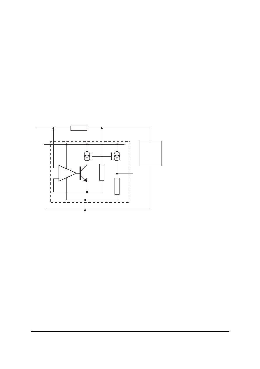
Basic operation
Load current from V
IN
is drawn through R
SENSE
developing a voltage V
SENSE
across the
ZXCT1051.
The internal amplifier forces V
SENSE
across internal resistance R
SH
causing a current to flow
through transistor Q1. This current is then converted to a voltage by R
G
. A ratio of 10:1 between
R
SH
and R
G
creates the fixed gain of 10 with an output impedance equal to R
G
(see electrical
characteristics for output current-voltage characteristics).
The gain equation of the ZXCT1051 is:
The maximum differential input voltage, V
SENSE
, is 150mV (I
L
* R
SENSE
); however voltages up to
500mV will not damage it. This can be increased further by the inclusion of a resistor, R
LIM
,
between V
SENSE
- pin and the load.
For best performance R
SENSE
should be connected as close to the V
SENSE
+ and V
SENSE
- pins thus
minimizing any series resistance with R
SENSE
.
R
SENSE
V
SENSE+
V
SENSE-
V
OUT
V
CC
V
RAIL
R
G
R
SH
Q1
GND
GND
Load
V
SENSE
I
L
R
SENSE
R
G
R
SH
----------- 1
◊
=