
DEVICE DESCRIPTION
The ZXFV401 provides the ability to separate out video
synchronisation signals for a wide variety of TV and CRT
display systems, standard and non-standard.
Flexibility arises from the use of just three external
resistors to adapt to each application. One resistor
controls a fully integrated internal colour carrier filter
with variable bandwidth. This filter aviods disturbance
from the colour carrier, permitting accurate threshold
slicing for timing extraction.
A second resistor controls the voltage threshold for
loss of signal detection after a time-out interval. The
third resistor controls the timing functions.
DC restoration for displays is facilitated by the Back
Porch synch output, which can be used to drive an
external curcuit to clamp the blanking voltage to a fixed
level.
FEATURES AND BENEFITS
∑
PAL, NTSC, SECAM, other TV systems
∑
Super accurate synch slice
∑
Variable filter for outputs: composite, horizontal,
Vertical, back porch, odd / even
∑
No-signal detector
∑
On chip sample / hold capacitors
∑
+5V single supply
∑
4.5 mA supply current
∑
Default vertical output where there are no
serration pulses
∑
Pin compatible with industry standard part SO16N
surface mount package
APPLICATIONS
∑
Digital image capture
∑
Video input systems requiring separation of
picture timing
∑
Video distribution
∑
CCTV surveillance
∑
Digital multimedia
∑
Timing for black level clamp
ZXFV401
PROVISIONAL ISSUE A - FEBRUARY 2002
1
SYNC SEPARATOR WITH VARIABLE FILTER
ORDERING INFORMATION
Part Number
Container
Increment
ZXFV401N16TA
Reel 7
500
ZXFV401N16TC
Reel 13
2500
3
1
2
4
5
6
7
8
9
10
11
12
13
14
15
16
ZXFV401N16
RFILT
RNOSIG
CSYNC
FILTIN
VSYNC
0VD
FILTOUT
FVIDIN
VLEV
NOSIG
BKPCH
RSET
ODDFLD
V+
HSYNC
0VA
+5V
C1
0.1uF
C2
0.1uF
RFILT
RNOSIG
COMPOSITE SYNC
HORIZONTAL SYNC
ODD FIELD
BACK PORCH
NO SIGNAL
SYNC TIP VOLTAGE
VERTICAL SYNC
RSET
VIDEO INPUT
75R
CONNECTION DIAGRAM

ABSOLUTE MAXIMUM RATINGS
Supply voltage VCC
-0.5V to +7V
Inputs to ground*
-0.5V to VCC +0.5V
Operating Temperature Range
-40 C to 85 C Storage -65 C to +150 C
Operating Ambient Junction temperature TJMAX150 C**
**The thermal resistance from the semiconductor die to ambient is typically 120 C/W when the SO16 package is
mounted on a PCB in free air. The power dissipation of the device when loaded must be designed to keep the
device junction temperature below TJMAX.
*During power-up and power-down, these voltage ratings require that signals be applied only when the power
supply is connected.
ZXFV401
PROVISIONAL ISSUE A - FEBRUARY 2002
2
PARAMETER
CONDITIONS
TEST
MIN
TYP
MAX
UNIT
DC Characteristics
Supply current
P
4.5
mA
Clamp voltage
Pin 4 unloaded
P
1.3
1.35
1.8
V
Discharge current at FILTIN
Pin 4, Vin = 2V pk-pk
C
1
A
Discharge current at FILTIN
Pin 4, no signal
P
3
6
12
A
Clamp charge current at FILTIN
Pin 4, Vin = 1V pk-pk
P
2
3
4
mA
Clamp voltage at FVIDIN
Pin 8 unloaded
P
1.3
1.35
1.8
V
Discharge current at FVIDIN
Pin 8, Vin = 2V pk-pk
C
1
Discharge current at FVIDIN
Pin 8, no signal
P
3
6
12
Clamp charge current at FVIDIN
Pin 8, Vin = 1V pk-pk
P
2
3
4
mA
RSET voltage, pin 12
P
1.5
1.75
2
V
RFILT voltage, pin 1
P
0.35
0.5
0.65
V
RNOSIG current, pin 2
P
1.5
2.5
3.5
A
Logic output Low voltage, VOL
IOL = 1.6mA
P
0.35
0.8
V
Logic output High voltage, VOH
IOH = 1.6mA
P
2.4
4
V
ELECTRICAL CHARACTERISTICS
V
CC
= 4.75 TO 5.25, R
SET
= 681k, R
FILT
= 22k, R
NOSIG
= 82k, T
amb
= 25 C unless otherwise stated.
TEST - P = production tested, C = characterised

ZXFV401
PROVISIONAL ISSUE A - FEBRUARY 2002
3
PARAMETER
CONDITIONS
TEST MIN
TYP
MAX
UNIT
AC Characteristics
FILTIN function input voltage range
PAL/NTSC
P
0.4
2
V pk-pk
Filter voltage gain
FILTIN to FILOUT
P
6
dB
Filter attenuation
4.4MHz for PAL,
3.6MHz for NTSC
C
12
dB
Slice level
Vin = 1V pk-pk
P
40
50
60
%
CSYNC prop. Delay, tCS
Relative to pin 4 input
P
250
400
ns
VSYNC delay
P
250
ns
VSYNC pulse width, tVSYNC (PAL)
P
165
s
VSYNC pulse width, tVSYNC (NTSC)
P
195
s
VSYNC default delay, tVSD
P
27
36
45
s
HSYNC delay
P
250
ns
HSYNC pulse width, tHSYNC
P
3.8
5
6.2
s
BKPCH delay, tBD
Relative to pin 4 input
P
250
400
ns
BKPCH pulse width, tB
P
2.7
3.7
4.7
s
VLEV output
Input 1 Vpk-pk, pin 4
P
500
600
700
mV
NOSIG time-out delay after loss of signal
P
600
s
ELECTRICAL CHARACTERISTICS (CONT)
VCC = 4.75 TO 5.25, R
SET
= 681k, R
FILT
= 22k, Tamb = 25 C unless otherwise stated.
TEST - P = production tested, C = characterised
ZXFV401
PROVISIONAL ISSUE A - FEBRUARY 2002
4
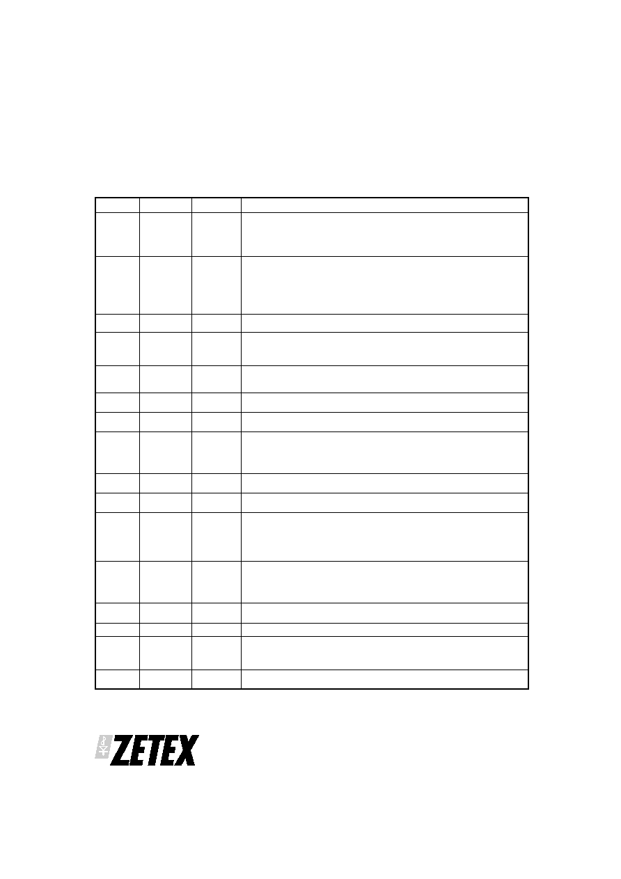
PIN No.
PIN NAME
TYPE
FUNCTION
1
RFILT
Resistor
control
Controls the input colour carrier filter characteristic.
An external
resistor RFILT connected from this pin to 0V sets the bandwidth.
Smaller RFILT gives increased bandwidth. See the detailed operating
description below.
2
RNOSIG
Resistor
control
Controls the no-signal detector level.
An external resistor RNOSIG
connected from this pin to 0V sets the threshold voltage level, according
to the equation
VPMIN = 0.75 RNOSIG / RSET
where VPMIN is the minimum detected sync pulse amplitude at pin 4
and RSET is the resistor value at pin 12.
3
CSYNC
Logic out
Composite sync logic output. Includes all sync pulses derived from the
input video.
4
FILTIN
Analog in
Input to colour carrier filter.
This is the main analog (unfiltered)
composite video input used when colour carrier filtering is required. A
voltage clamp circuit and adaptive current source are also included at
this node. See the detailed operating description.
5
VAYNC
Logic out
Vertical sync output. This is an active low pulse commencing on the first
vertical sync pulse trailing (rising) edge and ending near the second
next equalising pulse. See timing diagram.
6
OVD
Ground
Provides ground return path for internal logic output buffer circuits.
Normally connected externally to a common PCB ground plane.
7
FILTOUT
Analog out Analog output signal from colour carrier filter. The filter voltage gain is
nominally 2. This output is normally capacitor-coupled to pin 8.
8
FVIDIN
Analog in
Input for filtered analog video signal input. This is the direct input to the
sample/hold and sync slicing comparator providing the logic timing
edges. This input is normally coupled via an external capacitor from
FILTOUT, pin 7. It may be used as the signal input where the colour
carrier filter is not required. Includes a clamp similar that of pin 4.
9
VLEV
Analog out Analog output, a positive voltage typically equal to twice the (negative)
peak sync pulse amplitude if the filter is used.
10
NOSIG
Logic out
Logic output, which goes high after a time-out delay when no signal is
present. The threshold level is controlled at pin 2.
11
BKPCH
Logic out
Burst or Back Porch logic output, an active low monostable pulse
triggered from rising composite sync pulse edges. The width is set by
RSET to overlap most of the steady part of the back porch, assuming the
colour carrier burst has been attenuated sufficiently by filtering. This
pulse is then suitable for controlling an external black level clamping
circuit. See the timing diagram.
12
RSET
Resistor
control
Controls the timing interval of the sample/hold circuit and the
monostable interval for the sync outputs according to the application.
An external resistor, RSET connected from this pin to 0V establishes the
timing parameter, to which these times are scaled together. See the
detailed operating description.
13
ODDFLD
Logic out
Odd field logic output. High during an odd numbered field, low during
even. This output is timed with the start of the VSYNC pulse.
14
V+
Power in
Power supply input, +5V.
15
HSYNC
Logic out
Horizontal sync logic output. Monostable output derived from CSYNC
falling edges, it achieves a steady stream of 5µs pulses. The half line
events during the field blanking interval are eliminated. See timing
diagram.
16
OVA
Ground
Analog ground.
Normally connected externally to a common PCB
ground plane.
CONNECTIONS

DETAIL DESCRIPTION
Introduction
This device includes all the functions required to
separate out the critical timing points of most types of
video signal. A sample-and-hold process is used to
establish accurately the 50% point of the sync pulse.
The input is also filtered to avoid the effect of the colour
carrier. The filter is coupled externally. The following
paragraphs give a simplified description of the signal
processing.
Colour Carrier Filter
This is a low-pass filter providing adjustable
attenuation of the colour carrier with low distortion of
the remaining sync pulses so as to ensure accurate
timing of the extracted logic outputs. The control is via
an external resistor RFILT connected from pin 1 to
ground. A graph shows how the bandwidth varies with
the resistor value (Graph to be provide in future issue).
Clamping Circuits
Clamping circuits are use to limit the signal swing
excursion after AC coupling at both the input to the
filter, FILTIN and the timing extractor input, FVIDIN. In
each case, the sync tip level is maintained at a value of
nominally 1.35V.
Sync Timing Extraction Circuits
The waveforms are depicted in Timing Diagrams,
Figure 1 for PAL (625 lines) and Figure 2 for NTSC (525
lines).
Sample-and-hold circuits are used to obtain
time-delayed voltage values of the sync tip and the
back porch.
The sample gates are controlled by a
comparator sensing the video input relative to a
threshold at a fixed offset above the sync tip clamp
level.
The sampled voltages are combined in a
potential divider to derive the mean voltage (50%
amplitude), which is used as the sync pulse threshold.
A second comparator then provides CSYNC, the logic
version of the composite sync signal. This is delayed
slightly as shown in Figure 3.
The time delay
comprises that of the input filter and also the smaller
delay of the comparator and logic. The timing of the
sample hold and other time parameters are all
controlled together in unison by the external resistor
RSET. A 1% resistor tolerance is recommended. The
sync tip voltage level from the sample-and-hold is
buffered and provided as an analog output, VLEV.
The vertical sync output VSYNC is derived from the
Field pulse group. Where there are short equalisation
pulses in the standard systems, these short pulses are
ignored.
Essentially, a pulse width discriminator
circuit senses the first of the Field pulses, as they are
wider than those of the rest of the sequence.
The
trailing edge of the first negative-going Frame Pulse
(i.e. the rising edge of the first "serration" pulse)
triggers the VSYNC output. In systems with a frame
interval with no serration pulses, a vertical sync output
is provided after a default delay as in Figure 4. Also
provided is an ODDFLD logic output, which is high
during an odd-numbered field and low during an even
one.
The horizontal sync HSYNC is a monostable output
derived from the leading edge of the composite sync.
The pulse width is about 5 µs. Also, during the Field
blanking sequence, the additional half-line pulses are
removed by a timing circuit with a pulse interval
discrimination function controlled by RSET.
The Back Porch monostable output BKPCH is initiated
from the trailing edge of the composite.sync.
The
pulse is active low and the width is set according to
RSET.
Loss-of-Signal Detector
Loss of signal is indicated by a logic high level at the
output NOSIG. The decision threshold is set by an
external resistor RNOSIG connected from pin 2 to
ground.
The table of connections above gives the
equation used to determine a suitable resistor value. A
waiting time of nominally 600 µs occurs before the loss
of signal is flagged.
ZXFV401
PROVISIONAL ISSUE A - FEBRUARY 2002
5