SUMMARY
V
(BR)DSS
= 450V; R
DS(ON)
= 50 ; I
D
= 140mA
DESCRIPTION
This 450V enhancement mode N-channel MOSFET provides users with a
competitive specification offering efficient power handling capability, high
impedance and is free from thermal runaway and thermally induced
secondary breakdown. Applications benefiting from this device include a
variety of Telecom and general high voltage circuits.
FEATURES
∑
High voltage
∑
Low on-resistance
∑
Fast switching speed
∑
Low gate drive
∑
Low threshold
∑
SOT223 package variant engineered to increase spacing between
high voltage pins
APPLICATIONS
∑
Off-line power supply start-up circuitry
ORDERING INFORMATION
DEVICE
REEL SIZE
(inches)
TAPE WIDTH (mm)
QUANTITY
PER REEL
ZXMN0545G4TA
7
12mm embossed
1,000 units
ZXMN0545G4TC
13
12mm embossed
4,000 units
DEVICE MARKING
ZXMN
0545
ZXMN0545G4
ISSUE 1 - JANUARY 2006
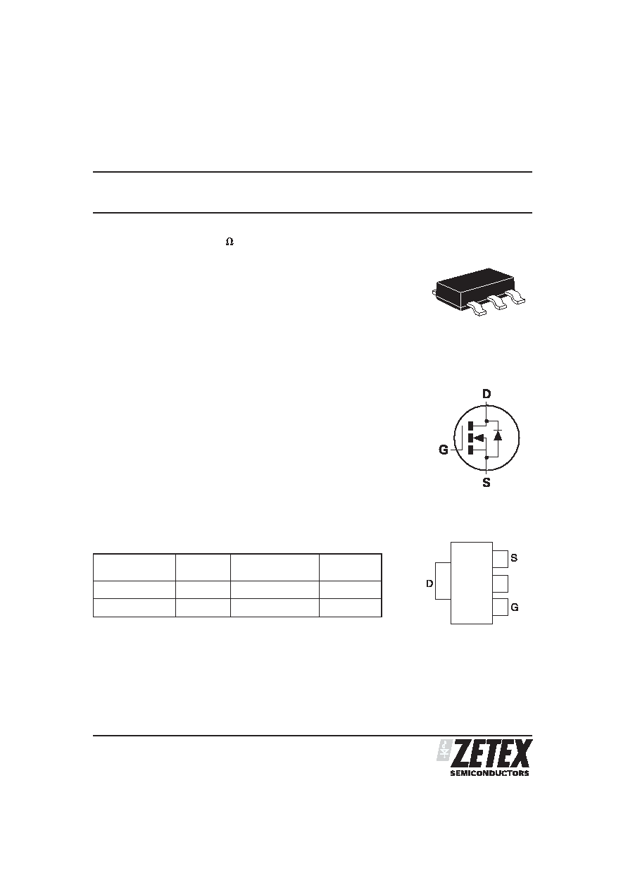
450V N-CHANNEL ENHANCEMENT MODE MOSFET
1
N/C
PINOUT - TOP VIEW
SOT223
ZXMN0545G4
ISSUE 1 - JANUARY 2006
2
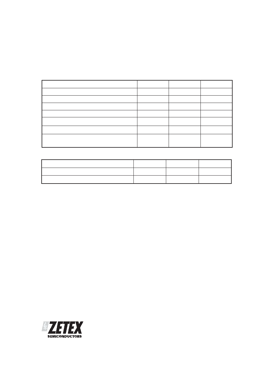
ABSOLUTE MAXIMUM RATINGS
PARAMETER
SYMBOL
VALUE
UNIT
Drain-Source Voltage
V
DS
450
V
Gate Source Voltage
V
GS
20
V
Continuous Drain Current (V
GS
=10V; T
amb
=25∞C)
(a)
I
D
140
mA
Pulsed Drain Current
(c)
I
DM
600
mA
Continuous Source Current (Body Diode)
(b)
I
S
140
A
Pulsed Source Current (Body Diode)
(c)
I
SM
600
A
Power Dissipation at T
amb
=25∞C
(a)
Linear derating factor
P
tot
2.0
1.6
W
mW/∞C
THERMAL RESISTANCE
PARAMETER
SYMBOL
VALUE
UNIT
Junction to Ambient
(a)
R
JA
62.5
∞C/W
Junction to Ambient
(b)
R
JA
32
∞C/W
NOTES:
(a) For a device surface mounted on 25mm x 25mm FR4 PCB with high coverage of single sided 1oz copper, in still air conditions
(b) For a device surface mounted on FR4 PCB measured at t 5 secs.
(c) Repetitive rating - pulse width limited by maximum junction temperature. Refer to Transient Thermal Impedance graph.

ZXMN0545G4
ISSUE 1 - JANUARY 2006
3
ELECTRICAL CHARACTERISTICS (at T
amb
= 25∞C unless otherwise stated)
PARAMETER
SYMBOL
MIN.
MAX.
UNIT
CONDITIONS
Drain-Source
Breakdown Voltage
BV
DSS
450
V
I
D
=1mA, V
GS
=0V
Gate-Source Threshold
Voltage
V
GS(th)
1
3
V
I
D
=1mA, V
DS
= V
GS
Gate-Body Leakage
I
GSS
20
nA
V
GS
=
20V, V
DS
=0V
Zero Gate Voltage Drain
Current
I
DSS
10
400
µA
µA
V
DS
=450 V, V
GS
=0V
V
DS
=405 V, V
GS
=0V,
T=125∞C
(2)
On-State Drain Current
(1)
I
D(on)
150
mA
V
DS
=25 V, V
GS
=10V
Static Drain-Source On-State
Resistance
(1)
R
DS(on)
50
V
GS
=10V, I
D
=100mA
Forward Transconductance
(1)(2)
g
fs
100
mS
V
DS
=25V, I
D
=100mA
Input Capacitance
(2)
C
iss
70
pF
Common Source Output
Capacitance
(2)
C
oss
10
pF
V
DS
=25V, V
GS
=0V, f=1MHz
Reverse Transfer Capacitance
(2)
C
rss
4
pF
Turn-On Delay Time
(2)(3)
t
d(on)
7
ns
V
DD
=25V, I
D
=100mA
Rise Time
(2)(3)
t
r
7
ns
Turn-Off Delay Time
(2)(3)
t
d(off)
16
ns
Fall Time
(2)(3)
t
f
10
ns
(1) Measured under pulsed conditions. Width=300
µs. Duty cycle 2%
(2) Sample test.
(3) Switching times measured with 50
source impedance and <5ns rise time on a pulse generator
ZXMN0545G4
ISSUE 1 - JANUARY 2006
4
No
r
m
a
l
i
s
e
d
R
n
o
(
S
D)
d
n
aV
G
S(
t
h)
0
4
-
0
8
0
6
0
4
0
2
0
0
2
-
0
2
1
0
6
1
0
4
1
0
0
1
4
.
2
2
.
2
0
.
2
8
.
1
6
.
1
4
.
1
2
.
1
0
.
1
6
.
0
8
.
0
i
a
r
D
S
-
n
c
r
u
o
e
R
s
e
is
c
n
a
t
e
R
D
(
S
on
)
G e
t
a
Th s
e
r
hold Vo tl
g
a e V
S
G ( h
t )
T
j
)
C
(
e
r
u
t
a
r
e
p
m
e
T
n
o
it
c
n
u
J
-
4
.
0
0
8
-
0
6
-
I
=
D
A
1
.
0
V
=
S
G
V
0
1
I
=
D
A
m
1
V
=
S
G
V
S
D
V
S
G
e
g
a
tl
o
V
e
c
r
u
o
S
e
t
a
G
-
)
s
t
l
o
V
(
R
S
D(
O
N
)
-D
ra
S
n
io
r
uc
e
e
R
s
i
st
a
n
ce
(
)
0
2
0
1
9
8
7
6
5
4
3
2
1
I
=
D
A
m
0
5
2
A
m
0
0
1
0
3
0
1
0
0
1
0
2
0
4
0
5
0
6
0
7
0
8
0
9
A
m
0
5
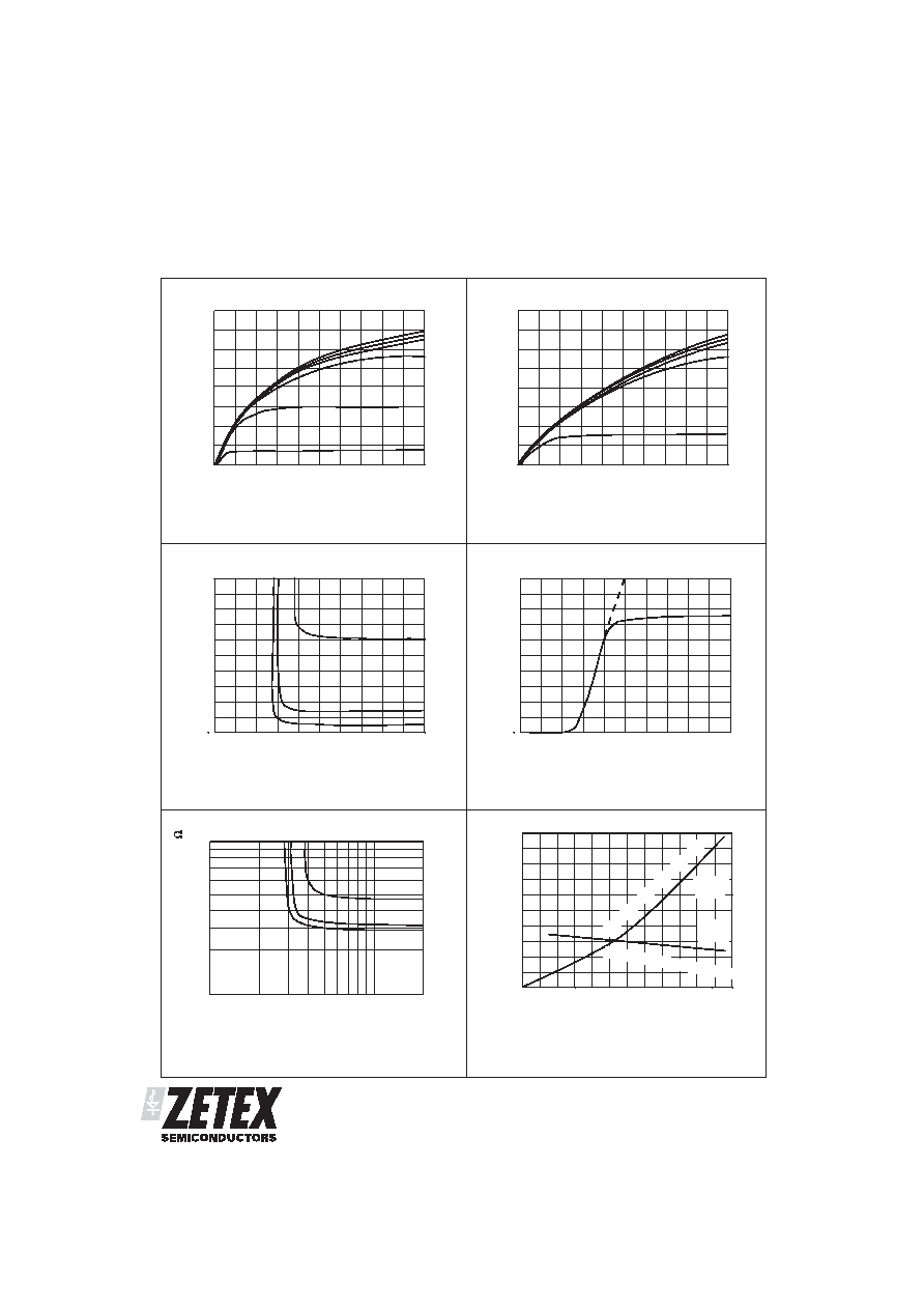
Output characteristics
Saturation characteristics
Voltage saturation characteristics
On-resistance vs gate-source voltage
Normalised R
DS(on)
and V
GS(th)
temperature
Transfer characteristics
V
S
D
e
c
r
u
o
S
n
i
a
r
D
-
)
s
t
l
o
V
(
e
g
a
t
l
o
V
I
D(
O
n
)
On-
St
a
r
D
e
t
ain
u
C
r
r
e
n
t
(
m
A)
V
-
S
D
e
c
r
u
o
S
n
i
a
r
D
Vg
a
t
l
oe
(
V
o
t
ls
)
V
-
S
G
e
g
a
tl
o
V
e
c
r
u
o
S
e
t
a
G
)
s
t
l
o
V
(
I
=
D
A
m
0
5
2
A
m
0
0
1
I
D(O
n
)
Dra
i
n
u
C
r
r
e
t
n
(
mA
)
V
-
S
G
e
c
r
u
o
S
e
t
a
G
)
s
t
l
o
V
(
e
g
a
t
l
o
V
I
D(
O
n
)
D
ra
i
C
nu
r
r
e
m
(
t
nA
)
V
S
D
e
c
r
u
o
S
n
i
a
r
D
-
)
s
t
l
o
V
(
e
g
a
t
l
o
V
A
m
0
5
0
1
8
6
4
2
0
1
9
8
7
6
5
4
3
2
1
0
V
=
S
D
V
5
2
0
0
1
0
9
0
8
0
7
0
6
0
5
0
4
0
3
0
2
0
1
0
0
2
6
1
2
1
8
4
0
2
1
0
4
8
6
1
0
2
V
0
1
V
6
V
4
V
3
V
S
G
=
0
0
8
0
0
6
0
0
2
0
0
0
4
0
0
7
0
0
5
0
0
3
0
0
1
V
8
V
5
V
0
1
V
6
V
4
V
3
V
S
G
=
0
0
0
2
0
0
4
0
0
3
0
0
1
V
5
0
0
3
0
0
0
1
0
0
2
0
0
4
0
0
5
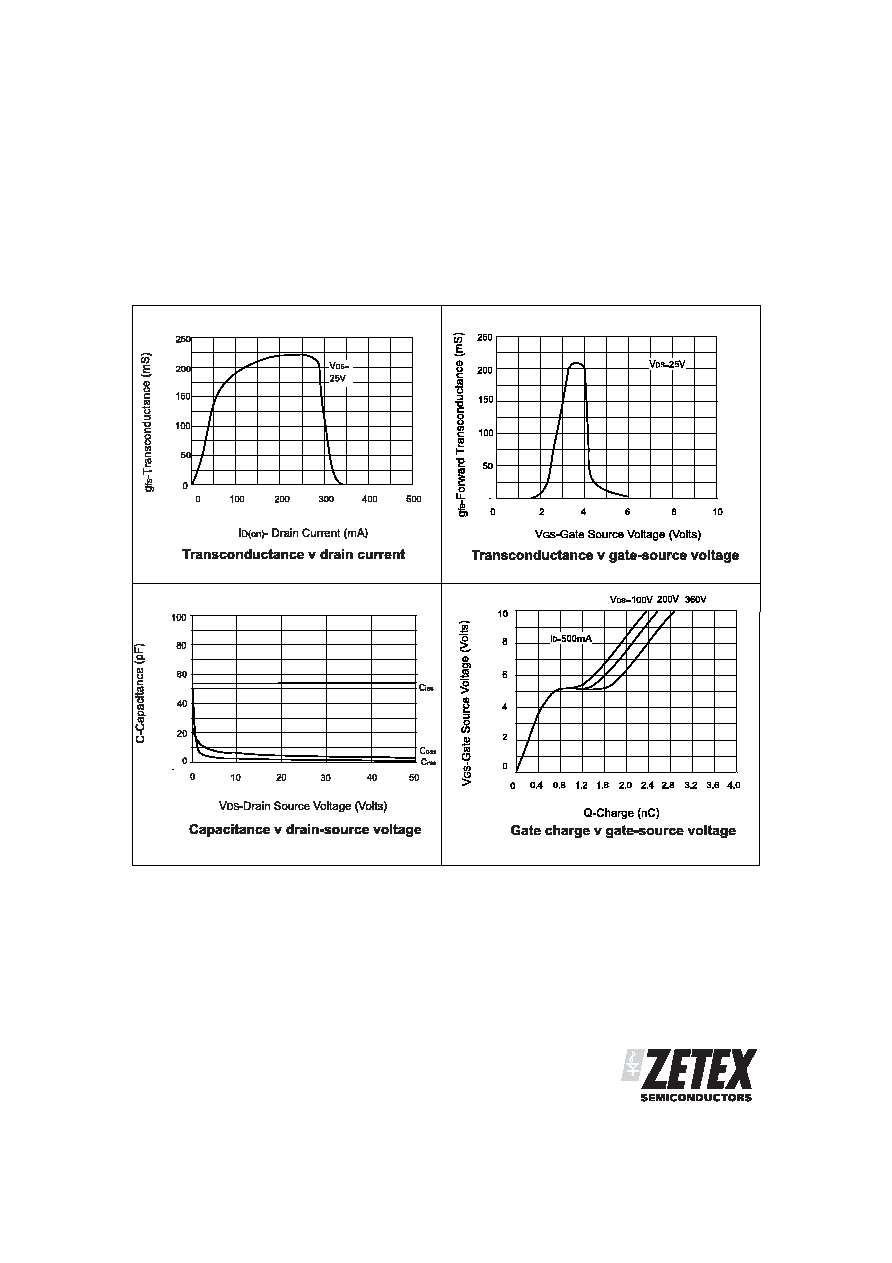
TYPICAL CHARACTERISTICS
ZXMN0545G4
ISSUE 1 - JANUARY 2006
5
TYPICAL CHARACTERISTICS