PROVISIONAL ISSUE D - AUGUST 2001
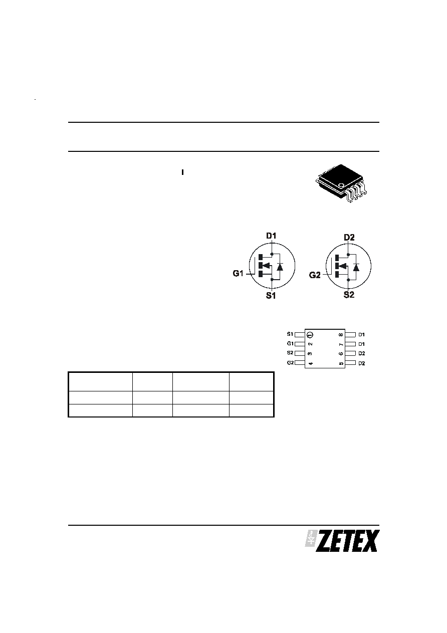
ZXMN6A09DN8
1
DUAL 60V N-CHANNEL ENHANCEMENT MODE MOSFET
SUMMARY
V
(BR)DSS
=60V; R
DS(ON)
=0.045
D
=5.2A
DESCRIPTION
This new generation of TRENCH MOSFETs from Zetex utilizes a unique
structure that combines the benefits of low on-resistance with fast
switching speed. This makes them ideal for high efficiency, low voltage,
power management applications.
FEATURES
∑
Low on-resistance
∑
Fast switching speed
∑
Low threshold
∑
Low gate drive
∑
Low profile SOIC package
APPLICATIONS
∑
DC - DC Converters
∑
Power Management Functions
∑
Disconnect switches
∑
Motor control
ORDERING INFORMATION
DEVICE
REEL SIZE
TAPE WIDTH
QUANTITY
PER REEL
ZXMN6A09DN8TA
7"
12mm
500 units
ZXMN6A09DN8TC
13"
12mm
2500 units
DEVICE MARKING
∑
ZXMN
6A09D
Top View
SO8
PROVISIONAL ISSUE D - AUGUST 2001
ZXMN6A09DN8
2
ABSOLUTE MAXIMUM RATINGS.
PARAMETER
SYMBOL
LIMIT
UNIT
Drain-Source Voltage
V
DSS
60
V
Gate Source Voltage
V
GS
20
V
Continuous Drain Current (V
GS
=10V; T
A
=25∞C)(b)(d)
(V
GS
=10V; T
A
=70∞C)(b)(d)
(V
GS
=10V; T
A
=25∞C)(a)(d)
I
D
5.2
4.1
3.9
A
Pulsed Drain Current (c)
I
DM
17.6
A
Continuous Source Current (Body Diode) (b)
I
S
3.5
A
Pulsed Source Current (Body Diode)(c)
I
SM
15
A
Power Dissipation at T
A
=25∞C (a)(d)
Linear Derating Factor
P
D
1.25
10
W
mW/∞C
Power Dissipation at T
A
=25∞C (a)(e)
Linear Derating Factor
P
D
1.81
14.5
W
mW/∞C
Power Dissipation at T
A
=25∞C (b)(d)
Linear Derating Factor
P
D
2.16
17.3
W
mW/∞C
Operating and Storage Temperature Range
T
j
:T
stg
-55 to +150
∞C
THERMAL RESISTANCE
PARAMETER
SYMBOL
VALUE
UNIT
Junction to Ambient (a)(d)
R
JA
100
∞C/W
Junction to Ambient (a)(e)
R
JA
69
∞C/W
Junction to Ambient (b)(d)
R
JA
58
∞C/W
NOTES
(a) For a device surface mounted on 25mm x 25mm FR4 PCB with high coverage of single sided 1oz copper,
in still air conditions
(b) For a device surface mounted on FR4 PCB measured at t 10 secs.
(c) Repetitive rating 25mm x 25mm FR4 PCB, D=0.05 pulse width=10µs - pulse width limited by maximum
junction temperature.
(d) For device with one active die
(e) For device with two active die running at equal power.

PROVISIONAL ISSUE D - AUGUST 2001
ZXMN6A09DN8
3
100m
1
10
100
10m
100m
1
10
Single Pulse
T
amb
=25∞ C
One active die
R
DS(on)
Limit
100µs
1ms
10ms
100ms
1s
DC
Safe Operating Area
I
D
Drain Current
(A)
V
DS
Drain-Source Voltage (V)
0
20
40
60
80
100
120
140
160
0.0
0.2
0.4
0.6
0.8
1.0
1.2
1.4
1.6
1.8
2.0
Two active die
One active die
Derating Curve
Temperature (∞ C)
Max Power Dissi
pation (W)
100µ
1m
10m 100m
1
10
100
1k
0
10
20
30
40
50
60
70
80
90
100
110
T
amb
=25∞ C
One active die
Transient Thermal Impedance
D=0.5
D=0.2
D=0.1
Single Pulse
D=0.05
Thermal Resistance (∞
C/W)
Pulse Width (s)
100µ
1m
10m 100m
1
10
100
1k
1
10
100
Single Pulse
T
amb
=25∞ C
One active die
Pulse Power Dissipation
Pulse Width (s)
Maximum Power
(W)
THERMAL CHARACTERISTICS
PROVISIONAL ISSUE D - AUGUST 2001
ZXMN6A09DN8
4
ELECTRICAL CHARACTERISTICS
(at T
A
= 25∞C unless otherwise stated).
PARAMETER
SYMBOL MIN.
TYP.
MAX.
UNIT CONDITIONS.
STATIC
Drain-Source Breakdown Voltage
V
(BR)DSS
60
V
I
D
=250
µ
A, V
GS
=0V
Zero Gate Voltage Drain Current
I
DSS
1
µ
A
V
DS
=60V, V
GS
=0V
Gate-Body Leakage
I
GSS
100
nA
V
GS
=
±
20V, V
DS
=0V
Gate-Source Threshold Voltage
V
GS(th)
1.0
V
I
D
=250
µ
A, V
DS
= V
GS
Static Drain-Source On-State Resistance
(1)
R
DS(on)
0.045
0.075
V
GS
=10V, I
D
=8.2A
V
GS
=4.5V, I
D
=7.4A
Forward Transconductance (3)
g
fs
15
S
V
DS
=15V,I
D
=8.2A
DYNAMIC (3)
Input Capacitance
C
iss
1407
pF
V
DS
=40 V, V
GS
=0V,
f=1MHz
Output Capacitance
C
oss
121
pF
Reverse Transfer Capacitance
C
rss
59
pF
SWITCHING(2) (3)
Turn-On Delay Time
t
d(on)
4.9
ns
V
DD
=15V, I
D
=3.5A
R
G
=6.0
, V
GS
=10V
(refer to test
circuit)
Rise Time
t
r
5.0
ns
Turn-Off Delay Time
t
d(off)
25.3
ns
Fall Time
t
f
4.6
ns
Gate Charge
Q
g
12.4
nC
V
DS
=15V,V
GS
=5V,
I
D
=3.5A
Total Gate Charge
Q
g
24.2
nC
V
DS
=15V,V
GS
=10V,
I
D
=3.5A
Gate-Source Charge
Q
gs
5.2
nC
Gate-Drain Charge
Q
gd
3.5
nC
SOURCE-DRAIN DIODE
Diode Forward Voltage (1)
V
SD
0.85
0.95
V
T
J
=25∞C, I
S
=6.6A,
V
GS
=0V
Reverse Recovery Time (3)
t
rr
26.3
ns
T
J
=25∞C, I
F
=3.5A,
di/dt= 100A/
µ
s
Reverse Recovery Charge (3)
Q
rr
26.6
nC
NOTES
(1) Measured under pulsed conditions. Width
=
300
µ
s. Duty cycle
2% .
(2) Switching characteristics are independent of operating junction temperature.
(3) For design aid only, not subject to production testing.
PROVISIONAL ISSUE D - AUGUST 2001
ZXMN6A09DN8
5
0.1
1
10
0.01
0.1
1
10
0.1
1
10
0.01
0.1
1
10
2
3
4
5
0.1
1
10
-50
0
50
100
150
0.4
0.6
0.8
1.0
1.2
1.4
1.6
1.8
1
10
0.1
1
0.4
0.6
0.8
1.0
1.2
0.1
1
10
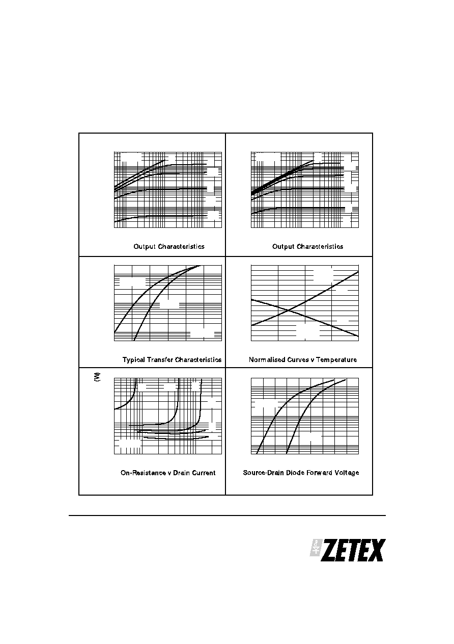
4V
5V
3.5V
2.5V
T = 25∞ C
3V
V
GS
I
D
Drain Current
(A)
V
DS
Drain-Source Voltage (V)
2V
2.5V
4V
5V
3V
T = 150∞ C
V
GS
3.5V
I
D
Drain Current
(A)
V
DS
Drain-Source Voltage (V)
V
DS
= 10V
T = 25∞ C
T = 150∞ C
I
D
Drain Current
(A)
V
GS
Gate-Source Voltage (V)
R
DS(on)
V
GS
= 10V
I
D
= 12A
V
GS(th)
V
GS
= V
DS
I
D
= 250uA
Normali
sed R
DS(on)
and V
GS(th)
Tj Junction Temperature (∞ C)
10V
4V
5V
3.5V
T = 25∞ C
3V
V
GS
R
DS(on)
Drain-Source On-Resist
ance
I
D
Drain Current (A)
T = 150∞ C
T = 25∞ C
V
SD
Source-Drain Voltage (V)
I
SD
Reverse Drain Current
(A)
TYPICAL CHARACTERISTICS