
SUMMARY
N Channel MOSFET--- V
(BR)DSS
=30V; R
SAT(on)
=0.18 ;
D
= 2.7A
Schottky Diode --- V
R
= 40V; V
F
= 500mV (@1A); I
C
=1A
DESCRIPTION
Packaged in the new innovation 3mm x 2mm MLP this combination dual
product comprises a low gate drive, low on-resistance N-Channel MOSFET
plus a fast-switching 1A Schottky barrier diode. This combination provides for
highly efficient performance in a range of applications, including DC-DC
conversion and low voltage power-management circuits.
Users will also gain several other key benefits:
Performance capability equivalent to much larger packages
Improved circuit efficiency & power levels
PCB area and device placement savings
Lower package height (0.9mm nom)
Reduced component count
FEATURES
∑
Low on-resistance
∑
Fast switching speed
∑
Low threshold
∑
Low gate drive
∑
Extremely Low VF, fast switching Schottky
∑
3mm x 2mm MLP
APPLICATIONS
∑
DC - DC Converters
∑
Low voltage power-management
DEVICE MARKING
MSA
ZXMNS3BM832
DRAFT ISSUE B - JUNE 2002
MPPSTM Miniature Package Power Solutions
30V N Channel MOSFET & 40V, 1A SCHOTTKY DIODE COMBINATION
DUAL
1
Cathode
Anode
DEVICE
REEL
TAPE
WIDTH
QUANTITY
PER REEL
ZXMNS3BM832TA
7
8mm
3000
ZXMNS3BM832TC
13
8mm
10000
ORDERING INFORMATION
3mm x 2mm Dual Die MLP
3mm x 2mm Dual MLP
underside view
PINOUT

ZXMNS3BM832
DRAFT ISSUE B - JUNE 2002
2
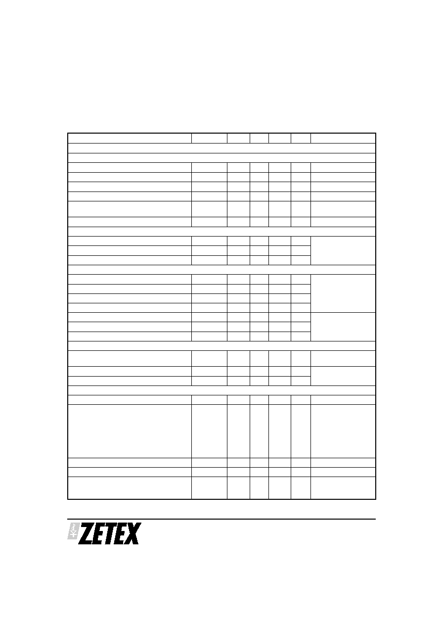
PARAMETER
SYMBOL
VALUE
UNIT
MOSFET
Drain-Source Voltage
V
DSS
30
V
Gate-Charge Voltage
V
GS
12
V
Continuous Drain Current@V
GS
=4.5V; T
A
=25 C (b)(d)
@V
GS
=4.5V; T
A
=70 C (b)(d)
@V
GS
=2.5V; T
A
=25 C (a)(d)
I
D
2.72
2.18
2.00
A
A
A
Pulsed Drain Current (c)
I
DM
t.b.a
A
Source Current (Body Diode) @T
A
=25 C (b)(d)
I
S
2.7
A
Pulsed Source Current (Body Diode)(c)
I
SM
t.b.a
A
Storage Temperature Range
T
stg
-55 to +150
∞C
Junction Temperature
T
j
150
∞C
Schottky Diode
Continuous Reverse Voltage
V
R
40
V
Forward Current
I
F
1
A
Non Repetitive Forward Current t
100
µ
s
t
10ms
I
FSM
12
5.2
A
A
Forward Voltage @ 1A
V
F
500
mV
Storage Temperature Range
T
stg
-55 to +150
∞C
Junction Temperature
T
j
125
∞C
ABSOLUTE MAXIMUM RATINGS.
Notes
(a) For a dual device surface mounted on 8 sq cm single sided 2oz copper on FR4 PCB, in still air conditions with all exposed pads attached. The
copper are is split down the centre line into two separate areas with one half connected to each half of the dual device.
(b) Measured at t<5 secs for a dual device surface mounted on 8 sq cm single sided 2oz copper on FR4 PCB, in still air conditions with all exposed
pads attached. The copper are is split down the centre line into two separate areas with one half connected to each half of the dual device.
(c) For a dual device surface mounted on 8 sq cm single sided 2oz copper on FR4 PCB, in still air conditions with minimal lead connections only.
(d) For a dual device surface mounted on 10 sq cm single sided 1oz copper on FR4 PCB, in still air conditions with all exposed pads attached
attached. The copper are is split down the centre line into two separate areas with one half connected to each half of the dual device.
(e) For a dual device surface mounted on 85 sq cm single sided 2oz copper on FR4 PCB, in still air conditions with all exposed pads attached
attached. The copper are is split down the centre line into two separate areas with one half connected to each half of the dual device.
(f) For a dual device with one active die.
(g) For dual device with 2 active die running at equal power.
(h) Repetitive rating - pulse width limited by max junction temperature. Refer to Transient Thermal Impedance graph.
(i) The minimum copper dimensions required for mounting are no smaller than the exposed metal pads on the base if the device as shown in the
package dimensions data. The thermal resistance for a dual device mounted on 1.5mm thick FR4 board using minimum copper 1 oz weight, 1mm
wide tracks and one half of the device active is Rth = 250∞C/W giving a power rating of Ptot = 500mW.

ZXMNS3BM832
DRAFT ISSUE B - JUNE 2002
3
PARAMETER
SYMBOL
VALUE
UNIT
Junction to Ambient (a)(f)
R
JA
83.3
∞C/W
Junction to Ambient (b)(f)
R
JA
43
∞C/W
Junction to Ambient (c)(f)
R
JA
125
∞C/W
Junction to Ambient (d)(f)
R
JA
111
∞C/W
Junction to Ambient (d)(g)
R
JA
73.5
∞C/W
Junction to Ambient (e)(g)
R
JA
41.7
∞C/W
THERMAL RESISTANCE
Notes
(a) For a dual device surface mounted on 8 sq cm single sided 2oz copper on FR4 PCB, in still air conditions with all exposed pads attached. The
copper are is split down the centre line into two separate areas with one half connected to each half of the dual device.
(b) Measured at t<5 secs for a dual device surface mounted on 8 sq cm single sided 2oz copper on FR4 PCB, in still air conditions with all exposed
pads attached. The copper are is split down the centre line into two separate areas with one half connected to each half of the dual device.
(c) For a dual device surface mounted on 8 sq cm single sided 2oz copper on FR4 PCB, in still air conditions with minimal lead connections only.
(d) For a dual device surface mounted on 10 sq cm single sided 1oz copper on FR4 PCB, in still air conditions with all exposed pads attached
attached. The copper are is split down the centre line into two separate areas with one half connected to each half of the dual device.
(e) For a dual device surface mounted on 85 sq cm single sided 2oz copper on FR4 PCB, in still air conditions with all exposed pads attached
attached. The copper are is split down the centre line into two separate areas with one half connected to each half of the dual device.
(f) For a dual device with one active die.
(g) For dual device with 2 active die running at equal power.
(h) Repetitive rating - pulse width limited by max junction temperature. Refer to Transient Thermal Impedance graph.
(i) The minimum copper dimensions required for mounting are no smaller than the exposed metal pads on the base if the device as shown in the
package dimensions data. The thermal resistance for a dual device mounted on 1.5mm thick FR4 board using minimum copper 1 oz weight, 1mm
wide tracks and one half of the device active is Rth = 250∞C/W giving a power rating of Ptot = 500mW.
PARAMETER
SYMBOL
VALUE
UNIT
Schottky
Power Dissipation at TA=25∞C (a)(d)
Linear Derating Factor
P
D
1.2
12
W
mW/∞C
Transistor
Power Dissipation at TA=25∞C (a)(f)
Linear Derating Factor
P
D
1.5
12
W
mW/∞C
Power Dissipation at TA=25∞C (b)(f)
Linear Derating Factor
P
D
2.9
23.2
W
mW/∞C
Power Dissipation at TA=25∞C (c)(f)
Linear Derating Factor
P
D
1
8
W
mW/∞C
Power Dissipation at TA=25∞C (d)(f)
Linear Derating Factor
P
D
1.13
8
W
mW/∞C
Power Dissipation at TA=25∞C (d)(g)
Linear Derating Factor
P
D
1.7
13.6
W
mW/∞C
Power Dissipation at TA=25∞C (e)(g)
Linear Derating Factor
P
D
3
24
W
mW/∞C
THERMAL PARAMETERS
ZXMNS3BM832
DRAFT ISSUE B - JUNE 2002
4
PARAMETER
SYMBOL
MIN.
TYP.
MAX.
UNIT CONDITIONS.
MOSFET
STATIC
Drain-Source Breakdown Voltage
V
(BR)DSS
30
V
I
D
=250
µ
A, V
GS
=0V
Zero Gate Voltage Drain Current
I
DSS
1
µ
A
V
DS
=30V, V
GS
=0V
Gate-Body Leakage
I
GSS
100
nA
V
GS
=
20V, V
DS
=0V
Gate-Source Threshold Voltage
V
GS(th)
0.7
V
I
D
=250 A, V
DS
= V
GS
Static Drain-Source On-State Resistance
(1)
R
DS(on)
0.13
0.17
0.18
0.25
V
GS
=4.5V, I
D
=1.5A
V
GS
=2.5V, I
D
=1.3A
Forward Transconductance (1)(3)
g
fs
t.b.a
S
V
DS
=15V,I
D
=1.5A
DYNAMIC (3)
Input Capacitance
C
iss
314
pF
V
DS
=15 V, V
GS
=0V,
f=1MHz
Output Capacitance
C
oss
40
pF
Reverse Transfer Capacitance
C
rss
23
pF
SWITCHING(2) (3)
Turn-On Delay Time
t
d(on)
1.1
ns
V
DD
=15V, I
D
=1A
R
G
=6.0
, V
GS
=4.5V
Rise Time
t
r
1.5
ns
Turn-Off Delay Time
t
d(off)
5.1
ns
Fall Time
t
f
2.1
ns
Total Gate Charge
Q
g
2.9
nC
V
DS
=15V,V
GS
=4.5V,
I
D
=1.5A
Gate-Source Charge
Q
gs
0.6
nC
Gate-Drain Charge
Q
gd
0.8
nC
SOURCE-DRAIN DIODE
Diode Forward Voltage (1)
V
SD
0.85
0.95
V
T
J
=25∞C, I
S
=1.7A,
V
GS
=0V
Reverse Recovery Time (3)
t
rr
17.7
ns
T
J
=25∞C, I
F
=2.7A,
di/dt= 100A/ s
Reverse Recovery Charge (3)
Q
rr
13.0
nC
SCHOTTKY DIODE ELECTRICAL CHARACTERISTICS
Reverse Breakdown Voltage
V
(BR)R
40
60
V
I
R
=300 A
Forward Voltage
V
F
240
265
305
355
390
425
495
420
270
290
340
400
450
500
600
--
mV
mV
mV
mV
mV
mV
mV
mV
I
F
=50mA*
I
F
=100mA*
I
F
=250mA*
I
F
=500mA*
I
F
=750mA*
I
F
=1000mA*
I
F
=1500mA*
I
F
=1000mA,T
a
=100∞C
Reverse Current
I
R
50
100
A
V
R
=30V
Diode Capacitance
C
D
25
pF
f=1MHz,V
R
=25V
Reverse Recovery Time
t
rr
12
ns
switched from
I
F
=500mA to I
R
=500mA
Measured at I
R
=50mA
ELECTRICAL CHARACTERISTICS (at T
amb
= 25∞C unless otherwise stated).
NOTES:
(1) Measured under pulsed conditions. Width
300
µ
s. Duty cycle
2% .
(2) Switching characteristics are independent of operating junction temperature.
(3) For design aid only, not subject to production testing.

Zetex plc
Fields New Road
Chadderton
Oldham, OL9 8NP
United Kingdom
Telephone (44) 161 622 4422
Fax: (44) 161 622 4420
Zetex GmbH
Streitfeldstraþe 19
D-81673 M¸nchen
Germany
Telefon: (49) 89 45 49 49 0
Fax: (49) 89 45 49 49 49
Zetex Inc
700 Veterans Memorial Hwy
Hauppauge, NY11788
USA
Telephone: (631) 360 2222
Fax: (631) 360 8222
Zetex (Asia) Ltd
3701-04 Metroplaza, Tower 1
Hing Fong Road
Kwai Fong
Hong Kong
Telephone: (852) 26100 611
Fax: (852) 24250 494
These offices are supported by agents and distributors in major countries world-wide.
This publication is issued to provide outline information only which (unless agreed by the Company in writing) may not be used, applied or reproduced
for any purpose or form part of any order or contract or be regarded as a representation relating to the products or services concerned. The Company
reserves the right to alter without notice the specification, design, price or conditions of supply of any product or service.
For the latest product information, log on to
www.zetex.com
© Zetex plc 2002
ZXMNS3BM832
DRAFT ISSUE B - JUNE 2002
5
CONTROLLING DIMENSIONS IN MILLIMETRES
APPROX. CONVERTED DIMENSIONS IN INCHES
MLP832 PACKAGE OUTLINE (3mm x 2mm Micro Leaded Package)
DIM
MILLIMETRES
INCHES
DIM
MILLIMETRES
INCHES
MIN.
MAX.
MIN.
MAX.
MIN.
MAX.
MIN.
MAX.
A
0.80
1.00
0.031
0.039
e
0.65 REF
0.0256 BSC
A1
0.00
0.05
0.00
0.002
E
2.00 BSC
0.0787 BSC
A2
0.65
0.75
0.0255
0.0295
E2
0.43
0.63
0.017
0.0249
A3
0.15
0.25
0.006
0.0098
E4
0.16
0.36
0.006
0.014
b
0.24
0.34
0.009
0.013
L
0.20
0.45
0.0078
0.0157
b1
0.17
0.30
0.0066
0.0118
L2
0.125
0.00
0.005
D
3.00 BSC
0.118 BSC
r
0.075 BSC
0.0029 BSC
D2
0.82
1.02
0.032
0.040
0
12
0
12
D3
1.01
1.21
0.0397
0.0476
MLP832 PACKAGE DIMENSIONS