SUMMARY
V
(BR)DSS
= -30V; R
DS(ON)
= 0.21
I
D
= -1.6A
DESCRIPTION
This new generation of trench MOSFETs from Zetex utilizes a unique structure that
combines the benefits of low on-resistance with fast switching speed. This makes
them ideal for high efficiency, low voltage, power management applications.
FEATURES
∑
Low on-resistance
∑
Fast switching speed
∑
Low threshold
∑
Low gate drive
∑
SOT23 package
APPLICATIONS
∑
DC - DC converters
∑
Power management functions
∑
Disconnect switches
∑
Motor control
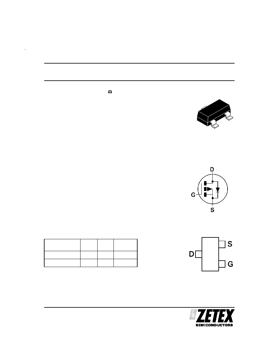
DEVICE MARKING
∑
313
ZXMP3A13F
PROVISIONAL ISSUE C - JULY 2004
1
30V P-CHANNEL ENHANCEMENT MODE MOSFET
DEVICE
REEL
SIZE
TAPE
WIDTH
QUANTITY
PER REEL
ZXMP3A13FTA
7"
8mm
3000 units
ZXMP3A13FTC
13"
8mm
10000 units
ORDERING INFORMATION
SOT23
Top View
PINOUT
ZXMP3A13F
PROVISIONAL ISSUE C - JULY 2004
2
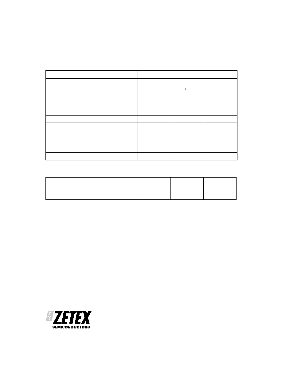
PARAMETER
SYMBOL
VALUE
UNIT
Junction to Ambient (a)
R
JA
200
∞C/W
Junction to Ambient (b)
R
JA
155
∞C/W
NOTES
(a) For a device surface mounted on 25mm x 25mm FR4 PCB with high coverage of single sided 1oz copper, in still air conditions
(b) For a device surface mounted on FR4 PCB measured at t 5 secs.
(c) Repetitive rating 25mm x 25mm FR4 PCB, D = 0.05, pulse width 10 s - pulse width limited by maximum junction temperature. Refer to
Transient Thermal Impedance graph.
THERMAL RESISTANCE
PARAMETER
SYMBOL
LIMIT
UNIT
Drain-Source Voltage
V
DSS
-30
V
Gate Source Voltage
V
GS
20
V
Continuous Drain Current V
GS
=10V; T
A
=25∞C (b)
V
GS
=10V; T
A
=70∞C (b)
V
GS
=10V; T
A
=25∞C (a)
I
D
-1.6
-1.3
-1.4
A
Pulsed Drain Current (c)
I
DM
-6
A
Continuous Source Current (Body Diode) (b)
I
S
-1.2
A
Pulsed Source Current (Body Diode) (c)
I
SM
-6
A
Power Dissipation at T
A
=25∞C (a)
Linear Derating Factor
P
D
625
5
mW
mW/∞C
Power Dissipation at T
A
=25∞C (b)
Linear Derating Factor
P
D
806
6.4
mW
mW/∞C
Operating and Storage Temperature Range
T
j
:T
stg
-55 to +150
∞C
ABSOLUTE MAXIMUM RATINGS
ZXMP3A13F
PROVISIONAL ISSUE C - JULY 2004
3
100m
1
10
10m
100m
1
10
Single Pulse
T
amb
=25∞C
R
DS(on)
Limited
100µs
1ms
10ms
100ms
1s
DC
Safe Operating Area
-I
D
D
r
a
i
n
C
u
rre
n
t
(
A
)
-V
DS
Drain-Source Voltage (V)
0
20
40
60
80
100 120 140 160
0.0
0.1
0.2
0.3
0.4
0.5
0.6
0.7
Derating Curve
Temperature (∞C)
M
a
x
Pow
e
r
D
i
s
s
i
pa
t
i
on
(
W
)
100µ
1m
10m 100m
1
10
100
1k
0
50
100
150
200
T
amb
=25∞C
Transient Thermal Impedance
D=0.5
D=0.2
D=0.1
Single Pulse
D=0.05
T
h
er
m
a
l
R
es
i
s
t
a
n
c
e
(
∞
C
/
W
)
Pulse Width (s)
100µ
1m
10m 100m
1
10
100
1k
1
10
Single Pulse
T
amb
=25∞C
Pulse Power Dissipation
Pulse Width (s)
M
axi
m
u
m
P
o
w
er
(
W
)
CHARACTERISTICS
ZXMP3A13F
PROVISIONAL ISSUE C - JULY 2004
4
PARAMETER
SYMBOL
MIN.
TYP.
MAX.
UNIT CONDITIONS
STATIC
Drain-Source Breakdown Voltage
V
(BR)DSS
-30
V
I
D
=-250 A, V
GS
=0V
Zero Gate Voltage Drain Current
I
DSS
-0.5
A
V
DS
=-30V, V
GS
=0V
Gate-Body Leakage
I
GSS
100
nA
V
GS
=
20V, V
DS
=0V
Gate-Source Threshold Voltage
V
GS(th)
-1.0
V
I
D
=-250 A, V
DS
= V
GS
Static Drain-Source On-State Resistance (1) R
DS(on)
0.210
0.330
V
GS
=-10V, I
D
=-1.4A
V
GS
=-4.5V, I
D
=-1.1A
Forward Transconductance (1)(3)
g
fs
2.48
S
V
DS
=-15V,I
D
=-1.4A
DYNAMIC (3)
Input Capacitance
C
iss
204
pF
V
DS
=-15V, V
GS
=0V,
f=1MHz
Output Capacitance
C
oss
39.8
pF
Reverse Transfer Capacitance
C
rss
25.8
pF
SWITCHING(2) (3)
Turn-On Delay Time
t
d(on)
1.5
ns
V
DD
=-15V, I
D
=-1A
R
G
=6.0 , V
GS
=-10V
Rise Time
t
r
2.8
ns
Turn-Off Delay Time
t
d(off)
11.3
ns
Fall Time
t
f
7.5
ns
Gate Charge
Q
g
2.58
nC
V
DS
=-15V,V
GS
=-5V,
I
D
=-1.4A
Total Gate Charge
Q
g
5.15
nC
V
DS
=-15V,V
GS
=-10V,
I
D
=-1.4A
Gate-Source Charge
Q
gs
0.65
nC
Gate-Drain Charge
Q
gd
0.92
nC
SOURCE-DRAIN DIODE
Diode Forward Voltage (1)
V
SD
-0.85
-0.95
V
T
J
=25∞C, I
S
=-1.1A,
V
GS
=0V
Reverse Recovery Time (3)
t
rr
18.6
ns
T
J
=25∞C, I
F
=-0.95A,
di/dt= 100A/
µs
Reverse Recovery Charge (3)
Q
rr
14.8
nC
ELECTRICAL CHARACTERISTICS
(at T
A
= 25∞C unless otherwise stated)
NOTES:
(1) Measured under pulsed conditions. Width
=300µs. Duty cycle 2% .
(2) Switching characteristics are independent of operating junction temperature.
(3) For design aid only, not subject to production testing.
ZXMP3A13F
PROVISIONAL ISSUE C - JULY 2004
5
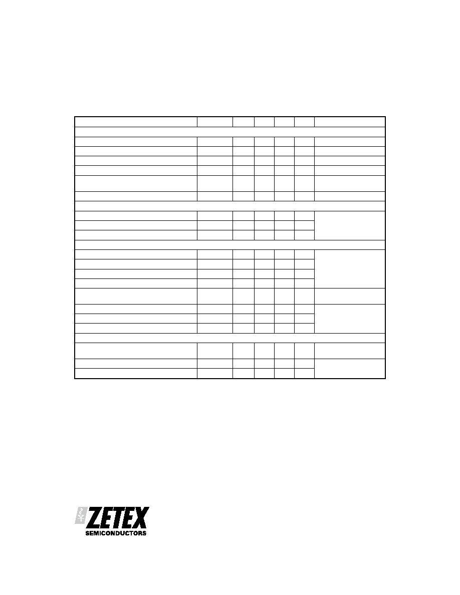
0.1
1
10
0.01
0.1
1
10
0.1
1
10
0.01
0.1
1
10
1
2
3
4
5
0.1
1
-50
0
50
100
150
0.6
0.8
1.0
1.2
1.4
1.6
0.1
1
10
0.1
1
10
100
0.2
0.4
0.6
0.8
1.0
1.2
1.4
0.01
0.1
1
10
5V
10V
4V
3.5V
-V
GS
2.5V
2V
3V
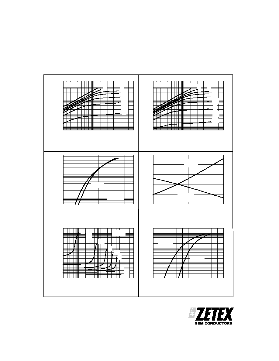
Output Characteristics
T = 25∞C
-V
GS
-I
D
Dr
a
i
n
C
u
r
r
e
n
t
(
A
)
-V
DS
Drain-Source Voltage (V)
5V
4V
3.5V
3V
2V
1.5V
10V
2.5V
Output Characteristics
T = 150∞C
-I
D
Dr
a
i
n
C
u
r
r
e
n
t
(
A
)
-V
DS
Drain-Source Voltage (V)
Typical Transfer Characteristics
-V
DS
= 10V
T = 25∞C
T = 150∞C
-I
D
Dr
a
i
n
C
u
r
r
e
n
t
(
A
)
-V
GS
Gate-Source Voltage (V)
Normalised Curves v Temperature
R
DS(on)
V
GS
= -10V
I
D
= -1.4A
V
GS(th)
V
GS
= V
DS
I
D
= -250uA
N
o
rm
a
lis
e
d
R
D
S
(
on)
an
d
V
G
S
(th
)
Tj Junction Temperature (∞C)
5V
10V
3V
2V
4V
3.5V
2.5V
On-Resistance v Drain Current
T = 25∞C
-V
GS
R
D
S
(
on)
D
r
ai
n
-
S
o
u
r
ce
O
n
-
R
esi
s
t
a
n
c
e
(
)
-I
D
Drain Current (A)
T = 150∞C
T = 25∞C
Source-Drain Diode Forward Voltage
-V
SD
Source-Drain Voltage (V)
-I
SD
R
ever
se
D
r
ai
n
C
u
r
r
e
n
t
(
A
)
TYPICAL CHARACTERISTICS