S E M I C O N D U C T O R S
DESCRIPTION
The ZXSC410 is voltage mode boost converter in SOT23-6 package. Its excellent
load and line regulation means that for the full supply range from lithium Ion cells,
the output voltage will typically change by less than 1%. Using high efficiency
Zetex switching transistors allow output voltages of tens of volts depending on the
selected transistor. The ZXSC420 includes a battery low indicator. This operates
by indicating when the converter is no longer able to maintain the regulated
output voltage rather than setting a preset threshold, thereby making it suitable for
various battery options and load currents.
FEATURES
∑
1.65V to 8V supply range
∑
Typical output regulation of ±1%
∑
Over 85% typical efficiency
∑
Output currents up to 300mA
∑
4.5 A typical shutdown current ZXSC410
∑
End of regulation output ZXSC420
APPLICATIONS
∑
System power for battery portable products
∑
LCD bias
∑
Local voltage conversion
DEVICE MARKING
∑
C410 ZXSC410
∑
C420 ZXSC420
ZXSC410
ZXSC420
ISSUE 2 - May 2003
1
VOLTAGE MODE BOOST CONVERTER
DEVICE
REEL
SIZE
TAPE
WIDTH
QUANTITY
PER REEL
ZXSC410E6TA
7"
8mm
3000 units
ZXSC420E6TA
7"
8mm
3000 units
ORDERING INFORMATION
SOT23-6
V
CC
GND
SENSE
DRIVE
STDN
V
FB
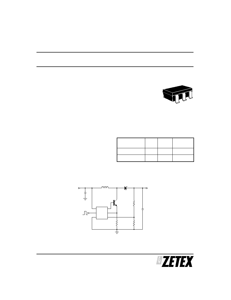
U1
ZXSC410
Q1
FMMT617
C2
D1
ZHCS1000
L1
C1
R2
R3
R1
V
IN
V
OUT
TYPICAL APPLICATIONS DIAGRAM
ABSOLUTE MAXIMUM RATINGS
V
CC
-0.3V
to
+10V
DRIVE
-0.3V
to
V
CC
+ 0.3V
EOR
-0.3V
to
V
CC
+ 0.3V
* (ZXSC420 only)
STDN
-0.3V
to
The lower of (+5.0V) or (V
CC
+ 0.3V)
* (ZXSC410 only)
V
FB
, SENSE
-0.3V
to
The lower of (+5.0V) or (V
CC
+ 0.3V)
Operating Temp.
-40∞C to
+85∞C
Storage Temp.
-55∞C to
+125∞C
Power Dissipation
450mW
ZXSC410
ZXSC420
S E M I C O N D U C T O R S
ISSUE 2 - May 2003
2
Symbol
Parameter
Conditions
Limits
Units
Min
Typ
Max
Supply parameters
V
CC
V
CC
Range
1.8
8
V
Iq
1
Quiescent Current
V
CC
= 8V
220
A
I
STDN
Shutdown Current
4.5
A
Eff
2
Efficiency
50mA > I
OUT
> 300mA
85
%
Acc
REF
Reference tolerance
1.8V < V
CC
< 8V
-3.0
3.0
%
TCO
REF
Reference Temp Co
0.005
%/ C
T
DRV
Discharge pulse width
1.8V < V
CC
< 8V
1.7
s
F
OSC
Operating Frequency
200
kHz
Input parameters
V
SENSE
sense voltage
22
28
34
mV
I
SENSE
sense input current
V
FB
=0V;V
SENSE
=0V
-1
-7
-15
A
V
FB
Feedback voltage
T
A
= 25∞C
291
300
309
mV
I
FB
2
Feedback input current
V
FB
=0V;V
SENSE
=0V
-1.2
-4.5
A
V
IH
Shutdown high voltage
1.5
1
V
CC
V
V
IL
Shutdown low voltage
0
0.55
V
dV
LN
Line voltage regulation
0.5
%/V
Output parameters
I
OUT
3
Output current
V
IN
> 2V, V
OUT
= V
IN
300
mA
I
DRIVE
Transistor drive current
V
DRIVE
= 0.7V
2
3.4
5
mA
V
DRIVE
Transistor voltage drive
1.8V < V
CC
< 8V
0
V
CC
-0.4
V
C
DRIVE
Mosfet gate drive cpbty
300
pF
VOH
EOR
EOR Flag output high
I
EOR
= -300nA
2.5
V
CC
V
VOL
EOR
EOR Flag output low
I
EOR
= 1mA
0
1.15
V
T
EOR
EOR delay time
T
A
= 25∞C
70
195
250
s
dI
LD
Load current regulation
0.01
%mA
ELECTRICAL CHARACTERISTICS
Test Conditions V
CC
= 3V, T= -40
∞
C to 85
∞
C unless otherwise stated.
Note
1
Excluding gate/base drive current.
2
I
FB
is typically half of these values at 3V
3
System not device spec, including recommended transistors.
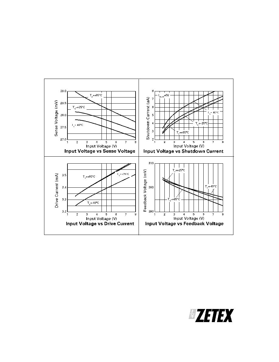
TYPICAL CHARACTERISTICS
ZXSC410
ZXSC420
S E M I C O N D U C T O R S
ISSUE 2 - May 2003
3
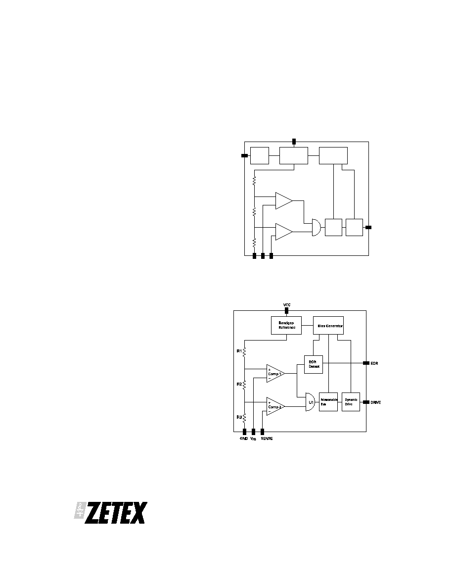
DEVICE DESCRIPTION
Bandgap Reference
All threshold voltages and internal currents are derived
from a temperature compensated bandgap reference
circuit with a reference voltage of 1.22V nominal.
Dynamic Drive Output
Depending on the input signal, the output is either
"LOW" or "HIGH". In the high state a 2.5mA current
source (max drive voltage = VCC-0.4V) drives the base
or gate of the external transistor. In order to operate the
external switching transistor at optimum efficiency,
both output states are initiated with a short transient
current in order to quickly discharge the base or the
gate of the switching transistor.
Switching Circuit
The switching circuit consists of two comparators,
Comp1 and Comp2, a gate U1, a monostable and the
drive output. Normally the DRIVE output is "HIGH"; the
external switching transistor is turned on. Current
ramps up in the inductor, the switching transistor and
external current sensing resistor. This voltage is
sensed by comparator, Comp2, at input I
SENSE
. Once
the current sense voltage across the sensing resistor
exceeds 20mV, comparator Comp2 through gate U1
triggers a re-triggerable monostable and turns off the
output drive stage for 2µs. The inductor discharges to
the load of the application. After 2µs a new charge cycle
begins, thus ramping the output voltage. When the
output voltage reaches the nominal value and V
FB
gets
an input voltage of more than 300mV, the monostable
is forced "on" from Comp1 through gate U1, until the
feedback voltage falls below 300mV. The above action
continues to maintain regulation.
EOR, End of Regulation Detector
The EOR circuit is a retriggerable 120µs monostable,
which is re-triggered by every down regulating action
of comparator Comp1. As long as regulation takes
place, output EOR is "HIGH" (high impedance, 100K to
V
CC
). Short dips of the output voltage of less than
120µs are ignored. If the output voltage falls below the
nominal value for more than 120µs, output EOR goes
"LOW". The reason for this to happen is usually a
slowly progressing drop of input voltage from the
discharging battery. Therefore the output voltage will
also start to drop slowly. With the EOR detector,
batteries can be used to the ultimate end of discharge,
with enough time left for a safe shutdown.
Block Diagrams
ZXSC410
ZXSC420
S E M I C O N D U C T O R S
ISSUE 2 - May 2003
4
+
_
+
_
R2
R3
R1
STDN
VCC
DRIVE
SENSE
GND V
FB
Shutdown
Bandgap
Reference
Bias Generator
Comp 1
Comp 2
U1
Dynamic
Drive
Monostable
2µs
Fig. 1 ZXSC410
Fig. 1 ZXSC420
APPLICATIONS INFORMATION
Switching transistor selection
The choice of switching transistor has a major impact
on the converter efficiency. For optimum performance,
a bipolar transistor with low V
CE(SAT)
and high gain is
required. The V
CEO
of the switching transistor is also an
important parameter as this sees the full output
voltage when the transistor is switched off. Zetex
SuperSOTTM transistors are an ideal choice for this
application.
Schottky diode selection
As with the switching transistor, the Schottky rectifier
diode has a major impact on the converter efficiency. A
Schottky diode with a low forward voltage and fast
recovery time should be used for this application.
The diode should be selected so that the maximum
forward current rating is greater or equal to the
maximum peak current in the inductor, and the
maximum reverse voltage is greater or equal to the
output voltage. The Zetex ZHCS Series meet these
needs.
Combination devices
To minimise the external component count Zetex
recommends the ZX3CDBS1M832 combination of
NPN transistor and Schottky diode in a 3mm x 2mm
MLP package. This device is recommended for use in
space critical applications.
The IC is also capable of driving MOSFETs. Zetex
recommends the ZXMNS3BM832 combination of low
threshold voltage N-Channel MOSFET and Schottky
diode in a 3mm x 2mm MLP package. This device is
recommended for use in space critical applications.
Inductor Selection
The inductor value must be chosen to satisfy
performance, cost and size requirements of the overall
solution.
Inductor selection has a significant impact on the
converter performance. For applications where
efficiency is critical, an inductor with a series resistance
of 500m
or less should be used.
A list of recommended inductors is listed in the table
below:
Peak current definition
In general, the I
PK
value must be chosen to ensure that
the switching transistor, Q1, is in full saturation with
maximum output power conditions, assuming
worse-case input voltage and transistor gain under all
operating temperature extremes.
Once I
PK
is decided the value of R
SENSE
can be
determined by:
R
SENSE
V
SENSE
I
PK
=
ZXSC410
ZXSC420
S E M I C O N D U C T O R S
ISSUE 2 - May 2003
5
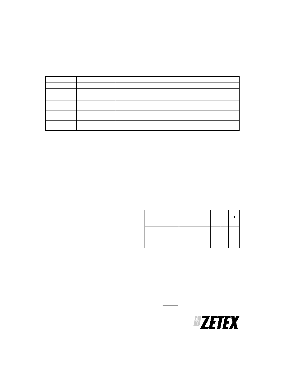
Pin No.
Name
Description
1
V
CC
Supply voltage, 1.8V to 8V.
2
GND
Ground
3
STDN/EOR
Shutdown ZXSC410 / End of regulation ZXSC420
4
SENSE
Inductor current sense input. Internal threshold voltage set to
28mV. Connect external sense resistor.
5
V
FB
Reference voltage. Internal threshold set to 300mV. Connect
external resistor network to set output voltage.
6
DRIVE
Drive output for external switching transistor. Connect to base or
gate of external switching transistor.
Part No.
Manufacture
L
I
PK
(A)
R
DC
( )
CMD4D11-100MC Sumida
10µH 0.5 0.457
CMD4D11-220MC Sumida
22µH 0.4 0.676
LPO2506OB-103
Coilcraft
10µH 1.0
0.24
ST2006103
Standex
Electronics Inc
10µH 0.6
0.1
PIN DESCRIPTIONS