 | –≠–ª–µ–∫—Ç—Ä–æ–Ω–Ω—ã–π –∫–æ–º–ø–æ–Ω–µ–Ω—Ç: ZXT790AK | –°–∫–∞—á–∞—Ç—å:  PDF PDF  ZIP ZIP |

1
S E M I C O N D U C T O R S
SUMMARY
BV
CEO
= -40V : R
SAT
= 83m ; I
C
= -3A
DESCRIPTION
Packaged in the D-Pak outline this high gain 40V PNP transistor offers low on state
losses making it ideal for use in DC-DC circuits and various driving and power
management functions.
FEATURES
∑
3 Amps continuous current
∑
Up to 6 Amps peak current
∑
Low saturation voltages
∑
High gain
APPLICATIONS
∑
DC - DC Converters
∑
MOSFET gate drivers
∑
Charging circuits
∑
Power switches
∑
Siren drivers
DEVICE MARKING
∑
ZXT790A
ZXT790AK
ISSUE 1 - JUNE 2003
40V PNP MEDIUM POWER HIGH GAIN TRANSISTOR IN D-PAK
DEVICE
REEL
SIZE
TAPE WIDTH
QUANTITY PER REEL
ZXT790AKTC
13"
16mm embossed
2500 units
ORDERING INFORMATION
PINOUT
DPAK
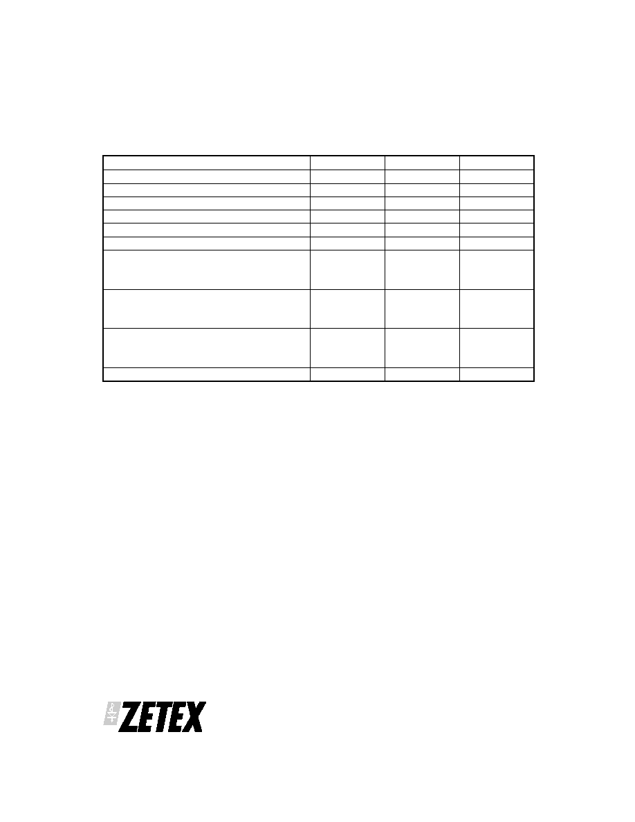
ZXT790AK
S E M I C O N D U C T O R S
ISSUE 1 - JUNE 2003
2
PARAMETER
SYMBOL
LIMIT
UNIT
Collector-Base Voltage
BV
CBO
-50
V
Collector-Emitter Voltage
BV
CEO
-40
V
Emitter-Base Voltage
BV
EBO
-5
V
Continuous Collector Current
I
C
-3
A
Peak Pulse Current
I
CM
-6
A
Base Current
I
B
-0.5
A
Power Dissipation at TA =25∞C
(a)
Linear Derating Factor
Thermal Resistance Junction to Ambient
P
D
2.1
16.8
59
W
mW/∞C
∞C/W
Power Dissipation at TA =25∞C
(b)
Linear Derating Factor
Thermal Resistance Junction to Ambient
P
D
3.0
24.4
41
W
mW/∞C
∞C/W
Power Dissipation at TA =25∞C
(c)
Linear Derating Factor
Thermal Resistance Junction to Ambient
P
D
3.9
30.9
32
W
mW/∞C
∞C/W
Operating and Storage Temperature Range
T
j
, T
stg
-55 to 150
∞C
NOTES
(a)
For a device surface mounted on 25mm x 25mm FR4 PCB with high coverage of single sided 1oz copper, in still
air conditions.
(b)
For a device surface mounted on 50mm x 50mm FR4 PCB with high coverage of single sided 1oz copper in still
air conditions.
(c)
For a device surface mounted on 50mm x 50mm FR4 PCB with high coverage of single sided 2oz copper in still
air conditions.
ABSOLUTE MAXIMUM RATINGS

ZXT790AK
S E M I C O N D U C T O R S
ISSUE 1 - JUNE 2003
3
CHARACTERISTICS
ZXT790AK
S E M I C O N D U C T O R S
ISSUE 1 - JUNE 2003
4
PARAMETER
SYMBOL
MIN.
TYP.
MAX.
UNIT CONDITIONS
Collector-Base Breakdown Voltage
BV
CBO
-50
-70
V
I
C
= -100 A
Collector-Emitter Breakdown Voltage
BV
CEO
-40
-60
V
I
C
= -10mA
(1)
Emitter-Base Breakdown Voltage
BV
EBO
-5
-8.3
V
I
E
= -100 A
Collector Cut-Off Current
I
CBO
<1
-20
nA
V
CB
= -30V
Collector Cut-Off Current
I
CE
S
<1
-20
nA
V
CB
= -30V
Emitter Cut-Off Current
I
EBO
<1
-20
nA
V
EB
= -4V
Collector-Emitter Saturation Voltage
V
CE(SAT)
-110
-220
-260
-250
-170
-350
-450
-450
mV
mV
mV
mV
I
C
= -0.5A, I
B
= -5mA
(1)
I
C
= -1A, I
B
= -10mA
(1)
I
C
= -2A, I
B
= -50mA
(1)
I
C
= -3A, I
B
= -300mA
(1)
Base-Emitter Saturation Voltage
V
BE(SAT)
-1.05
-1.15
V
I
C
= -3A, IB = -300mA
(1)
Base-Emitter Turn-On Voltage
V
BE(ON)
-0.9
-1.0
V
I
C
= -3A, VCE = -2V
(1)
Static Forward Current Transfer Ratio
h
FE
300
250
200
150
80
450
390
350
280
170
800
I
C
= -10mA, V
CE
= -2V
(1)
I
C
= -500mA, V
CE
= -2V
(1)
I
C
= -1A, V
CE
= -2V
(1)
I
C
= -2A, V
CE
= -2V
(1)
I
C
= -3A, V
CE
= -2V
(1)
Transition Frequency
f
T
100
MHz I
C
= -50mA, V
CE
= -5V
f = 50MHz
Output Capacitance
C
OBO
24
pF
V
CB
= -10V, f = 1MHz
(1)
Switching Times
t
ON
t
OFF
35
600
ns
ns
I
C
= -500mA, V
CC
= -10V,
I
B1
= I
B2
= -50mA
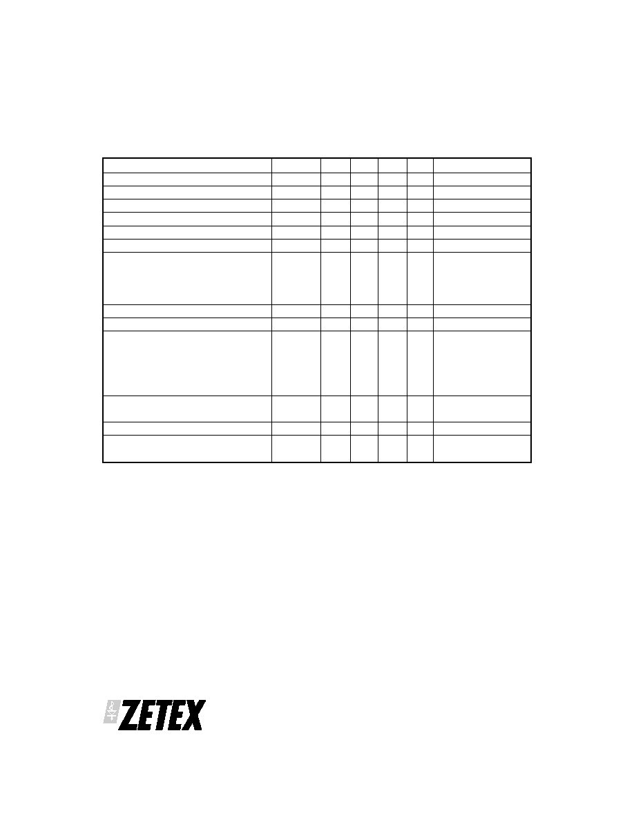
ELECTRICAL CHARACTERISTICS (at T
amb
= 25∞C unless otherwise stated)
NOTES
(1)
Measured under pulsed conditions. Pulse width
300 s; duty cycle
2%.
ZXT790AK
S E M I C O N D U C T O R S
ISSUE 1 - JUNE 2003
5
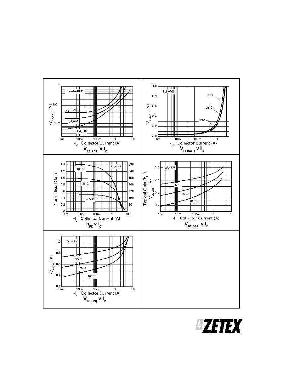
TYPICAL CHARACTERISTICS