1
S E M I C O N D U C T O R S
SUMMARY
BV
CEO
= -100V : R
SAT
= 67m ; I
C
= -5A
DESCRIPTION
Packaged in the D-Pak outline this high current high performance 100V PNP
transistor offers low on state losses making it ideal for use in DC-DC circuits
and various driving and power management functions.
FEATURES
∑
5 amps continuous current
∑
Up to 10 amps peak current
∑
Low equivalent on resistance
∑
Low saturation voltages
APPLICATIONS
∑
DC - DC converters
∑
DC - DC modules
∑
Power switches
∑
Motor control
∑
Automotive circuits
∑
Inverter circuits
DEVICE MARKING
∑
ZXT953
ZXT953K
ISSUE 1 - DECEMBER 2003
100V PNP LOW SATURATION MEDIUM POWER TRANSISTOR IN D-PAK
DEVICE
REEL
SIZE
TAPE
WIDTH
QUANTITY PER
REEL
ZXT953KTC
13"
16mm
2500 units
ORDERING INFORMATION
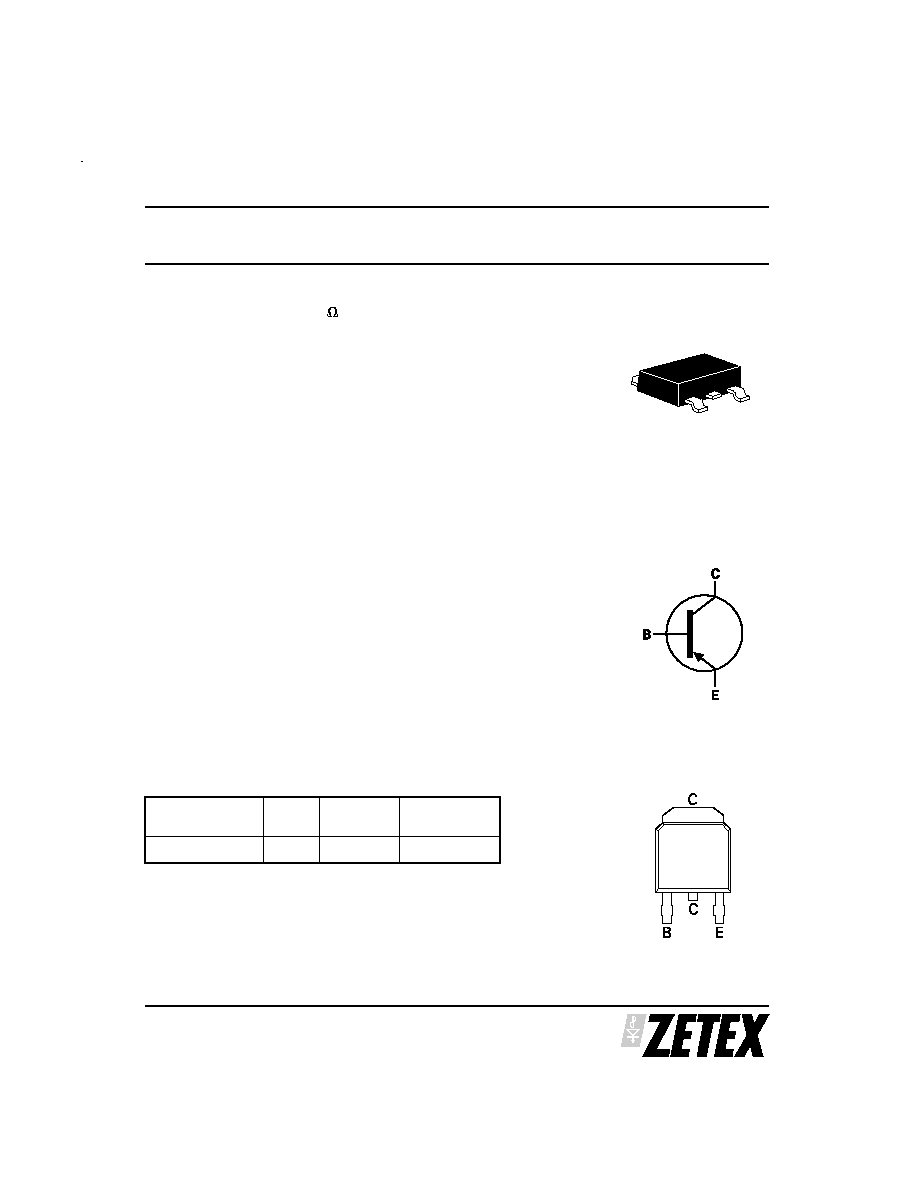
PINOUT
TOP VIEW
DPAK
ZXT953K
S E M I C O N D U C T O R S
ISSUE 1 - DECEMBER 2003
2
PARAMETER
SYMBOL
VALUE
UNIT
Junction to ambient
(a)
R
JA
59
∞C/W
Junction to ambient
(b)
R
JA
39
∞C/W
Junction to ambient
(c)
R
JA
30
∞C/W
NOTES
(a) For a device surface mounted on 25mm x 25mm x 1.6mm FR4 PCB with high coverage of single sided 1oz copper, in still air conditions.
(b) For a device surface mounted on 50mm x 50mm x 1.6mm FR4 PCB with high coverage of single sided 1oz copper, in still air conditions.
(c) For a device surface mounted on 50mm x 50mm x 1.6mm FR4 PCB with high coverage of single sided 2oz copper, in still air conditions.
THERMAL RESISTANCE
PARAMETER
SYMBOL
LIMIT
UNIT
Collector-base voltage
BV
CBO
-140
V
Collector-base voltage
BV
CER
-140
V
Collector-emitter voltage
BV
CEO
-100
V
Emitter-base voltage
BV
EBO
-7
V
Peak pulse current
I
CM
-10
A
Continuous collector current
(b)
I
C
-5
A
Base current
I
B
-0.5
A
Power dissipation at T
A
=25∞C
(a)
Linear derating factor
P
D
2.1
16.8
W
mW/∞C
Power dissipation at T
A
=25∞C
(b)
Linear derating factor
P
D
3.2
25.6
W
mW/∞C
Power dissipation at T
A
=25∞C
(c)
Linear derating factor
P
D
4.2
33.6
W
mW/∞C
Operating and storage temperature range
T
j
, T
stg
-55 to +150
∞C
ABSOLUTE MAXIMUM RATINGS

ZXT953K
S E M I C O N D U C T O R S
ISSUE 1 - DECEMBER 2003
4
PARAMETER
SYMBOL
MIN.
TYP.
MAX.
UNIT CONDITIONS
Collector-base breakdown voltage
BV
CBO
-140
-170
V
I
C
= -100 A
Collector-emitter breakdown voltage
BV
CER
-140
-170
V
I
C
= -1 A, R
BE
=
1k
Collector-emitter breakdown voltage
BV
CEO
-100
-125
V
I
C
= -10mA*
Emitter-base breakdown voltage
BV
EBO
-7
-8.1
V
I
E
= -100 A
Collector cut-off current
I
CBO
1
-20
nA
V
CB
= -100V
Collector cut-off current
I
CER
1
-20
nA
V
CB
= -100V, R
BE
=
1k
Emitter cut-off current
I
EBO
1
-10
nA
V
EB
= -6V
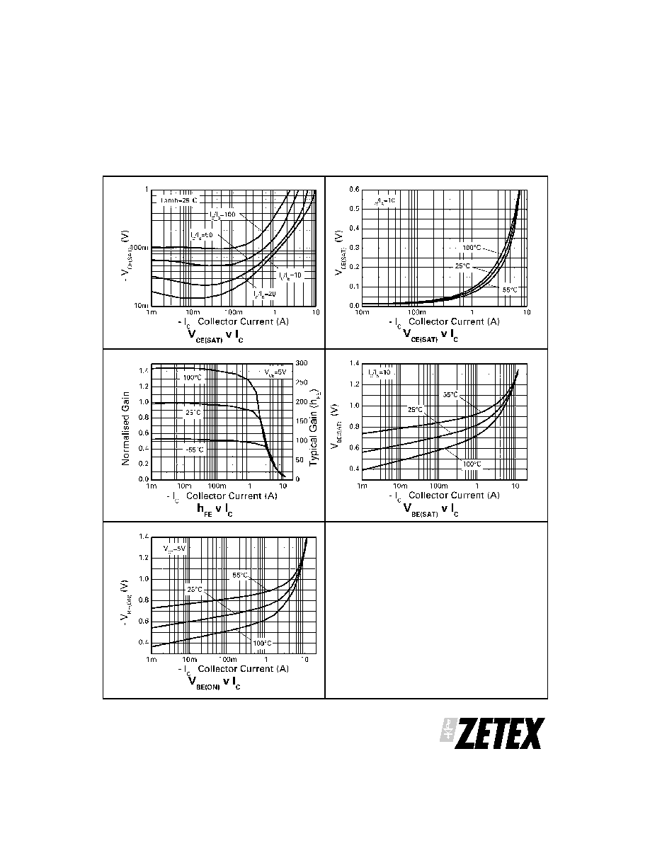
Collector-emitter saturation voltage
V
CE(SAT)
-20
-80
-140
-335
-30
-100
-175
-390
mV
mV
mV
mV
I
C
= -0.1A, I
B
= -10mA*
I
C
= -1A, I
B
= -100mA*
I
C
= -2A, I
B
= -200mA*
I
C
= -5A, I
B
= -500mA*
Base-emitter saturation voltage
V
BE(SAT)
-1.01
-1.1
mV
I
C
= -5A, I
B
= -500mA*
Base-emitter turn-on voltage
V
BE(ON)
-0.94
-1.05
mV
I
C
= -5A, V
CE
= -1V*
Static forward current transfer ratio
h
FE
100
100
50
15
225
200
85
30
15
300
I
C
= -10mA, V
CE
= -1V*
I
C
= -1A, V
CE
= -1V*
I
C
= -3A, V
CE
= -1V*
I
C
= -5A, V
CE
= -1V*
I
C
= -10A, V
CE
= -1V*
Transition frequency
f
T
125
MHz I
C
= -100mA, V
CE
= -10V
f = 50MHz
Output capacitance
C
OBO
65
pF
V
CB
= -10V, f = 1MHz*
Switching times
t
ON
t
OFF
110
460
nS
nS
I
C
= -2A, V
CC
= -10V,
I
B1
= I
B2
= -200mA
ELECTRICAL CHARACTERISTICS (at T
amb
= 25∞C unless otherwise stated)
* Measured under pulsed conditions. Pulse width
300 s; duty cycle
2%.