 | –≠–ª–µ–∫—Ç—Ä–æ–Ω–Ω—ã–π –∫–æ–º–ø–æ–Ω–µ–Ω—Ç: ZXTDCM832 | –°–∫–∞—á–∞—Ç—å:  PDF PDF  ZIP ZIP |

SUMMARY
V
CEO
=50V; R
SAT
= 68m ; I
C
= 4A
DESCRIPTION
Packaged in the innovative 3mm x 2mm MLP (Micro Leaded Package) outline,
these new 4
th
generation low saturation dual transistors offer extremely low on
state losses making them ideal for use in DC-DC circuits and various driving
and power management functions.
Additionally users gain several other key benefits:
Performance capability equivalent to much larger packges
Improved circuit efficiency & power levels
PCB area and device placement savings
Lower package height (nom 0.9mm)
Reduced component count
FEATURES
∑
Low Equivalent On Resistance
∑
Extremely Low Saturation Voltage (100mV @1A)
∑
h
FE
characterised up to 6A
∑
I
C
=4A Continuous Collector Current
∑
3mm x 2mm MLP
APPLICATIONS
∑
DC - DC Converters
∑
Charging circuits
∑
CCFL Backlighting
∑
Power switches
∑
Motor control
DEVICE MARKING
DCC
ZXTDCM832
ISSUE 1 - JUNE 2002
1
MPPSTM Miniature Package Power Solutions
DUAL 50V NPN SILICON LOW SATURATION SWITCHING TRANSISTOR
B2
C2
E2
B1
C1
E1
3mm x 2mm MLP
underside view
PINOUT
DEVICE
REEL
TAPE
WIDTH
QUANTITY
PER REEL
ZXTDCM832TA
7
8mm
3000
ZXTDCM832TC
13
8mm
10000
ORDERING INFORMATION
3mm x 2mm (Dual die) MLP

ZXTDCM832
ISSUE 1 - JUNE 2002
2
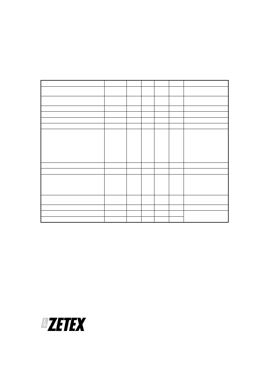
PARAMETER
SYMBOL
VALUE
UNIT
Junction to Ambient (a)(f)
R
JA
83.3
∞C/W
Junction to Ambient (b)(f)
R
JA
51
∞C/W
Junction to Ambient (c)(f)
R
JA
125
∞C/W
Junction to Ambient (d)(f)
R
JA
111
∞C/W
Junction to Ambient (d)(g)
R
JA
73.5
∞C/W
Junction to Ambient (e)(g)
R
JA
41.7
∞C/W
THERMAL RESISTANCE
Notes
(a) For a dual device surface mounted on 8 sq cm single sided 2oz copper on FR4 PCB, in still air conditions with all exposed pads attached. The
copper area is split down the centre line into two separate areas with one half connected to each half of the dual device.
(b) Measured at t<5 secs for a dual device surface mounted on 8 sq cm single sided 2oz copper on FR4 PCB, in still air conditions with all exposed
pads attached. The copper area is split down the centre line into two separate areas with one half connected to each half of the dual device.
(c) For a dual device surface mounted on 8 sq cm single sided 2oz copper on FR4 PCB, in still air conditions with minimal lead connections only.
(d) For a dual device surface mounted on 10 sq cm single sided 1oz copper on FR4 PCB, in still air conditions with all exposed pads attached
attached. The copper area is split down the centre line into two separate areas with one half connected to each half of the dual device.
(e) For a dual device surface mounted on 85 sq cm single sided 2oz copper on FR4 PCB, in still air conditions with all exposed pads attached
attached. The copper area is split down the centre line into two separate areas with one half connected to each half of the dual device.
(f) For a dual device with one active die.
(g) For dual device with 2 active die running at equal power.
(h) Repetitive rating - pulse width limited by max junction temperature. Refer to Transient Thermal Impedance graph.
(i) The minimum copper dimensions required for mounting are no smaller than the exposed metal pads on the base of the device as shown in the
package dimensions data. The thermal resistance for a dual device mounted on 1.5mm thick FR4 board using minimum copper 1 oz weight, 1mm
wide tracks and one half of the device active is Rth = 250∞C/W giving a power rating of Ptot = 500mW.
PARAMETER
SYMBOL
LIMIT
UNIT
Collector-Base Voltage
V
CBO
100
V
Collector-Emitter Voltage
V
CEO
50
V
Emitter-Base Voltage
V
EBO
7.5
V
Peak Pulse Current
I
CM
6
A
Continuous Collector Current (a)(f)
I
C
4
A
Base Current
I
B
1000
mA
Power Dissipation at TA=25∞C (a)(f)
Linear Derating Factor
P
D
1.5
12
W
mW/∞C
Power Dissipation at TA=25∞C (b)(f)
Linear Derating Factor
P
D
2.45
19.6
W
mW/∞C
Power Dissipation at TA=25∞C (c)(f)
Linear Derating Factor
P
D
1
8
W
mW/∞C
Power Dissipation at TA=25∞C (d)(f)
Linear Derating Factor
P
D
1.13
9
W
mW/∞C
Power Dissipation at TA=25∞C (d)(g)
Linear Derating Factor
P
D
1.7
13.6
W
mW/∞C
Power Dissipation at TA=25∞C (e)(g)
Linear Derating Factor
P
D
3
24
W
mW/∞C
Operating and Storage Temperature Range
T
j
:T
stg
-55 to +150
∞C
ABSOLUTE MAXIMUM RATINGS.

ZXTDCM832
ISSUE 1 - JUNE 2002
3
0.1
1
10
100
0.01
0.1
1
10
0
25
50
75
100
125
150
0.0
0.5
1.0
1.5
2.0
2.5
3.0
3.5
100µ
1m
10m 100m
1
10
100
1k
0
20
40
60
80
0.1
1
10
100
0
25
50
75
100
125
150
175
200
225
0.1
1
10
100
0.0
0.5
1.0
1.5
2.0
2.5
3.0
3.5
Note (a)(f)
100us
100ms
1s
V
CE(SAT)
Limited
1ms
Safe Operating Area
Single Pulse, T
amb
=25∞C
DC
10ms
I
C
C
o
l
l
e
c
t
o
r
C
u
rre
n
t
(
A
)
V
CE
Collector-Emitter Voltage (V)
1oz Cu
Note (d)(f)
1oz Cu
Note (d)(g)
2oz Cu
Note (a)(f)
2oz Cu
Note (e)(g)
Derating Curve
T
amb
=25∞C
M
a
x
P
ow
e
r
D
i
s
s
i
pa
t
i
on
(
W
)
Temperature (∞C)
Note (a)(f)
D=0.2
D=0.5
D=0.1
Transient Thermal Impedance
Single Pulse
D=0.05
T
h
e
r
m
a
l
R
e
si
st
a
n
ce
(
∞
C
/
W
)
Pulse Width (s)
1oz copper
Note (g)
1oz copper
Note (f)
2oz copper
Note (f)
2oz copper
Note (g)
Thermal Resistance v Board Area
T
h
e
r
m
a
l
R
e
si
st
a
n
ce
(
∞
C
/
W
)
Board Cu Area (sqcm)
1oz copper
Note (g)
2oz copper
Note (g)
1oz copper
Note (f)
2oz copper
Note (f)
Power Dissipation v Board Area
T
amb
=25∞C
T
j max
=150∞C
Continuous
P
D
D
i
s
s
i
pa
t
i
on
(
W
)
Board Cu Area (sqcm)
TYPICAL CHARACTERISTICS
ZXTDCM832
ISSUE 1 - JUNE 2002
4
PARAMETER
SYMBOL
MIN.
TYP.
MAX.
UNIT
CONDITIONS.
Collector-Base Breakdown
Voltage
V
(BR)CBO
100
190
V
I
C
=100 A
Collector-Emitter Breakdown
Voltage
V
(BR)CEO
50
65
V
I
C
=10mA*
Emitter-Base Breakdown Voltage
V
(BR)EBO
7.5
8.2
V
I
E
=100 A
Collector Cut-Off Current
I
CBO
25
nA
V
CB
=80V
Emitter Cut-Off Current
I
EBO
25
nA
V
EB
=6V
Collector Emitter Cut-Off Current
I
CES
25
nA
V
CES
=40V
Collector-Emitter Saturation
Voltage
V
CE(sat)
10
70
145
115
225
270
20
100
200
220
300
320
mV
mV
mV
mV
mV
mV
I
C
=0.1A, I
B
=10mA*
I
C
=1A, I
B
=50mA*
I
C
=1A, I
B
=10mA*
I
C
=2A, I
B
=50mA*
I
C
=3A, I
B
=100mA*
I
C
=4A, I
B
=200mA*
Base-Emitter Saturation Voltage
V
BE(sat)
1.00
1.05
V
I
C
=4A, I
B
=200mA*
Base-Emitter Turn-On Voltage
V
BE(on)
0.94
1.00
V
I
C
=4A, V
CE
=2V*
Static Forward Current Transfer
Ratio
h
FE
200
300
200
100
400
450
400
225
40
I
C
=10mA, V
CE
=2V*
I
C
=0.2A, V
CE
=2V*
I
C
=1A, V
CE
=2V*
I
C
=2A, V
CE
=2V*
I
C
=6A, V
CE
=2V*
Transition Frequency
f
T
100
165
MHz
I
C
=50mA, V
CE
=10V
f=100MHz
Output Capacitance
C
obo
12
20
pF
V
CB
=10V, f=1MHz
Turn-On Time
t
(on)
170
ns
V
CC
=10V, I
C
=1A
I
B1
=I
B2
=10mA
Turn-Off Time
t
(off)
750
ns
ELECTRICAL CHARACTERISTICS (at T
amb
= 25∞C unless otherwise stated).
*Measured under pulsed conditions. Pulse width=300
µ
s. Duty cycle
2%

ZXTDCM832
ISSUE 1 - JUNE 2002
5
1m
10m
100m
1
10
1m
10m
100m
1m
10m
100m
1
10
0.00
0.05
0.10
0.15
0.20
0.25
1m
10m
100m
1
10
0.0
0.2
0.4
0.6
0.8
1.0
1.2
1m
10m
100m
1
10
0.4
0.6
0.8
1.0
1m
10m
100m
1
10
0.4
0.6
0.8
1.0
0
90
180
270
360
450
540
630
V
CE(SAT)
v I
C
Tamb=25∞C
I
C
/I
B
=100
I
C
/I
B
=50
I
C
/I
B
=10
V
CE
(
S
A
T
)
(V
)
I
C
Collector Current (A)
V
BE(SAT)
v I
C
I
C
/I
B
=50
100∞C
25∞C
-55∞C
V
CE
(
S
A
T
)
(V
)
I
C
Collector Current (A)
h
FE
v I
C
V
CE
=2V
-55∞C
25∞C
100∞C
N
o
r
m
a
lis
e
d
G
a
in
I
C
Collector Current (A)
25∞C
V
CE(SAT)
v I
C
I
C
/I
B
=50
100∞C
-55∞C
V
BE
(
S
A
T
)
(V
)
I
C
Collector Current (A)
V
BE(ON)
v I
C
V
CE
=2V
100∞C
25∞C
-55∞C
V
B
E
(
ON)
(V
)
I
C
Collector Current (A)
Typ
i
c
a
l
G
a
i
n
(
h
FE
)
TYPICAL CHARACTERISTICS

ZXTDCM832
ISSUE 1 - JUNE 2002
6
Europe
Zetex plc
Fields New Road
Chadderton
Oldham, OL9 8NP
United Kingdom
Telephone (44) 161 622 4422
Fax: (44) 161 622 4420
uksales@zetex.com
Zetex GmbH
Streitfeldstraþe 19
D-81673 M¸nchen
Germany
Telefon: (49) 89 45 49 49 0
Fax: (49) 89 45 49 49 49
europe.sales@zetex.com
Americas
Zetex Inc
700 Veterans Memorial Hwy
Hauppauge, NY11788
USA
Telephone: (631) 360 2222
Fax: (631) 360 8222
usa.sales@zetex.com
Asia Pacific
Zetex (Asia) Ltd
3701-04 Metroplaza, Tower 1
Hing Fong Road
Kwai Fong
Hong Kong
Telephone: (852) 26100 611
Fax: (852) 24250 494
asia.sales@zetex.com
These offices are supported by agents and distributors in major countries world-wide.
This publication is issued to provide outline information only which (unless agreed by the Company in writing) may not be used, applied or reproduced
for any purpose or form part of any order or contract or be regarded as a representation relating to the products or services concerned. The Company
reserves the right to alter without notice the specification, design, price or conditions of supply of any product or service.
For the latest product information, log on to
www.zetex.com
© Zetex plc 2002
CONTROLLING DIMENSIONS IN MILLIMETRES
APPROX. CONVERTED DIMENSIONS IN INCHES
MLP832 PACKAGE OUTLINE (3mm x 2mm Micro Leaded Package)
DIM
MILLIMETRES
INCHES
DIM
MILLIMETRES
INCHES
MIN.
MAX.
MIN.
MAX.
MIN.
MAX.
MIN.
MAX.
A
0.80
1.00
0.031
0.039
e
0.65 REF
0.0256 BSC
A1
0.00
0.05
0.00
0.002
E
2.00 BSC
0.0787 BSC
A2
0.65
0.75
0.0255
0.0295
E2
0.43
0.63
0.017
0.0249
A3
0.15
0.25
0.006
0.0098
E4
0.16
0.36
0.006
0.014
b
0.24
0.34
0.009
0.013
L
0.20
0.45
0.0078
0.0157
b1
0.17
0.30
0.0066
0.0118
L2
0.125
0.00
0.005
D
3.00 BSC
0.118 BSC
r
0.075 BSC
0.0029 BSC
D2
0.82
1.02
0.032
0.040
0
12
0
12
D3
1.01
1.21
0.0397
0.0476
MLP832 PACKAGE DIMENSIONS