1
S E M I C O N D U C T O R S
SUMMARY
NPN --- V
CEO
= 80V; R
SAT
=
68m ; I
C
= 3.5A
DESCRIPTION
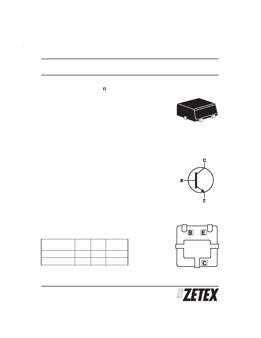
Packaged in the new
innovative 2mm x 2mm MLP (Micro Leaded
Package)
outline, these new 4
th
generation low saturation dual PNP transistors offer
extremely low on state losses making them ideal for use in DC-DC circuits and
various driving and power management functions.
Additionally users gain several other key benefits:
Performance capability equivalent to much larger packages
Improved circuit efficiency & power levels
PCB area and device placement savings
Lower Package Height (0.9mm nom)
Reduced component count
FEATURES
∑
Low Equivalent On Resistance
∑
Extremely Low Saturation Voltage (185mV max @1A)
∑
h
FE
specified up to 5A
∑
I
C
=-3.5A Continuous Collector Current
∑
2mm x 2mm MLP
APPLICATIONS
∑
DC - DC Converters
∑
DC - DC Modules
∑
Power switches
∑
Motor control
DEVICE MARKING
∑
SE
ZXTEM322
ISSUE 1 - JUNE 2003
MPPS
TM
Miniature Package Power Solutions
80V NPN LOW SATURATION TRANSISTOR
DEVICE
REEL
SIZE
TAPE
WIDTH
QUANTITY
PER REEL
ZXTEM322TA
7"
8mm
3000
ZXTEM322TC
13"
8mm
10000
ORDERING INFORMATION
Underside View
MLP322
ZXTEM322
S E M I C O N D U C T O R S
ISSUE 1 - JUNE 2003
2
PARAMETER
SYMBOL
VALUE
UNIT
Junction to Ambient
(a)
R
JA
83
C/W
Junction to Ambient
(b)
R
JA
51
C/W
Junction to Ambient
(d)
R
JA
125
C/W
Junction to Ambient
(e)
R
JA
42
C/W
NOTES
(a) For a single device surface mounted on
10
sq cm 1oz copper on FR4 PCB, in still air conditions with all exposed pads attached.
(b) For a single device surface mounted on
10
sq cm 1oz copper on FR4 PCB, in still air conditions measured at t 5 secs with all exposed pads
attached.
(c) Repetitive rating - pulse width limited by max junction temperature. Refer to Transient Thermal Impedance graph.
(d) For a single device surface mounted on 10 sq cm 1oz copper FR4 PCB, in still air conditions with minimal lead connections only.
(e) For a single device surface mounted on 65 sq cm 2oz copper FR4 PCB, in still air conditions with all exposed pads attached.
(f) The minimum copper dimensions required for mounting are no smaller than the exposed metal pads on the base of the device, as shown in
the package dimensions data. The thermal resistance for a device mounted on 1.5mm thick FR4 board using minimum copper of 1oz weight and
1mm wide tracks is Rth= 300∞C/W giving a power rating of Ptot=420mW
THERMAL RESISTANCE
PARAMETER
SYMBOL
LIMIT
UNIT
Collector-Base Voltage
V
CBO
100
V
Collector-Emitter Voltage
V
CEO
80
V
Emitter-Base Voltage
V
EBO
7.5
V
Peak Pulse Current
I
CM
5
A
Continuous Collector Current
(a)
I
C
3.5
A
Base Current
I
B
1000
mA
Power Dissipation at TA=25∞C
(a)
Linear Derating Factor
P
D
1.5
12
W
mW/ C
Power Dissipation at TA=25∞C
(b)
Linear Derating Factor
P
D
2.45
19.6
W
mW/ C
Power Dissipation at TA=25∞C
(d)
Linear Derating Factor
P
D
1
8
W
mW/ C
Power Dissipation at TA=25∞C
(e)
Linear Derating Factor
P
D
3
24
W
mW/ C
Operating & Storage Temperature Range
T
j
:T
stg
-55 to +150
C
Junction Temperature
T
j
150
C
ABSOLUTE MAXIMUM RATINGS
ZXTEM322
S E M I C O N D U C T O R S
ISSUE 1 - JUNE 2003
3
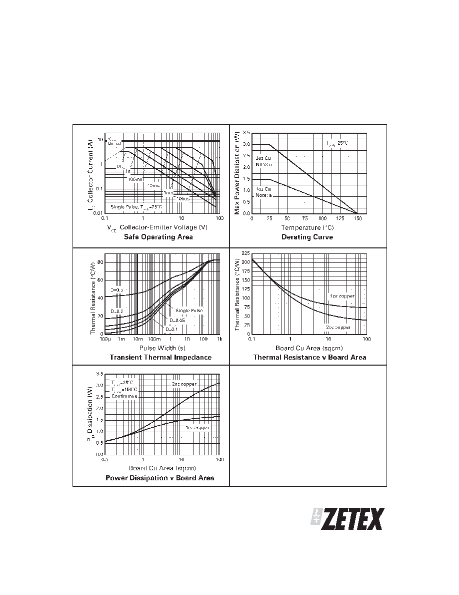
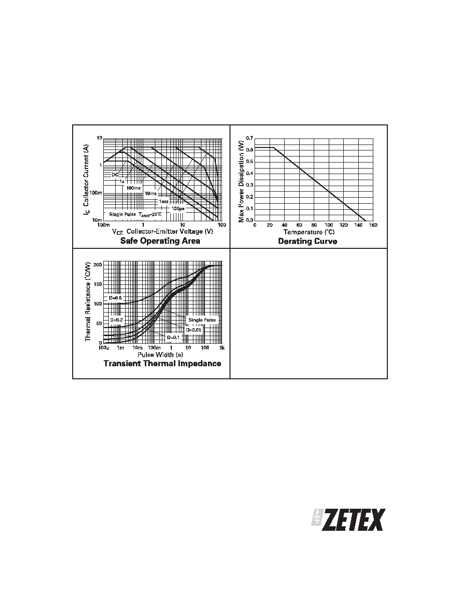
TYPICAL CHARACTERISTICS
ZXTEM322
S E M I C O N D U C T O R S
ISSUE 1 - JUNE 2003
4
PARAMETER
SYMBOL
MIN.
TYP.
MAX.
UNIT CONDITIONS
Collector-Base Breakdown Voltage
V
(BR)CBO
100
180
V
I
C
=100 A
Collector-Emitter Breakdown Voltage
V
(BR)CEO
80
110
V
I
C
=10mA*
Emitter-Base Breakdown Voltage
V
(BR)EBO
7.5
8.2
V
I
E
=100 A
Collector Cut-Off Current
I
CBO
25
nA
V
CB
=80V
Emitter Cut-Off Current
I
EBO
25
nA
V
EB
=6V
Collector Emitter Cut-Off Current
I
CES
25
nA
V
CE
=65V
Collector-Emitter Saturation Voltage
V
CE(sat)
15
45
145
160
240
20
60
185
200
325
mV
mV
mV
mV
mV
I
C
=0.1A, I
B
=10mA*
I
C
=0.5A, I
B
=50mA*
I
C
=1A, I
B
=20mA*
I
C
=1.5A, I
B
=50mA*
I
C
=3.5A, I
B
=300mA*
Base-Emitter Saturation Voltage
V
BE(sat)
1.09
1.175
V
I
C
=3.5A, I
B
=300mA*
Base-Emitter Turn-On Voltage
V
BE(on)
0.96
1.05
V
I
C
=3.5A, V
CE
=2V*
Static Forward Current Transfer Ratio
h
FE
200
300
110
60
20
450
450
170
90
30
10
900
I
C
=10mA, V
CE
=2V*
I
C
=200mA, V
CE
=2V*
I
C
=1A, V
CE
=2V*
I
C
=1.5A, V
CE
=2V*
I
C
=3A, V
CE
=2V*
I
C
=5A, V
CE
=2V*
Transition Frequency
f
T
100
160
MHz I
C
=50mA, V
CE
=10V
f=100MHz
Output Capacitance
C
obo
11.5
18
pF
V
CB
=10A, f=1MHz
Turn-On Time
t
(on)
86
ns
V
CC
=10V, I
C
=1A
I
B1
=I
B2
=25mA
Turn-Off Time
t
(off)
1128
ns
ELECTRICAL CHARACTERISTICS (at T
amb
= 25∞C unless otherwise stated)
*Measured under pulsed conditions. Pulse width=300 s. Duty cycle
2%
ZXTEM322
S E M I C O N D U C T O R S
ISSUE 1 - JUNE 2003
5
TYPICAL CHARACTERISTICS