Issue 1 - February 2006
1
www.zetex.com
© Zetex Semiconductors plc 2006
ZXTN25020DFH
20V SOT23 NPN medium power transistor
Summary
BV
CEX
> 100V; BV
(BR)CEO
> 20V
BV
ECO
> 5V;
I
C(CONT)
= 4.5A
R
CE(sat)
= 28 m typical
V
CE(sat)
< 43 mV @ 1A;
P
D
= 1.25W
Complementary part number ZXTP25020DFH
Description
Advanced process capability and package design have been used to
maximize the power handling and performance of this small outline
transistor. The compact size and ratings of this device make it ideally
suited to applications where space is at a premium.
Features
∑
Higher power dissipation SOT23 package
∑
High peak current
∑
Low saturation voltage
∑
100V forward blocking voltage
∑
5V reverse blocking voltage
Applications
∑
DC - DC converters
∑
MOSFET and IGBT gate driving
∑
LED driver
∑
Motor drive
∑
Relay, lamp and solenoid drive
Ordering information
Device marking
016
Device
Reel size
(inches)
Tape width
Quantity per reel
ZXTN25020DFHTA
7
8mm
3000
C
E
Pinout - top view
B

ZXTN25020DFH
Issue 1 - February 2006
2
www.zetex.com
© Zetex Semiconductors plc 2006
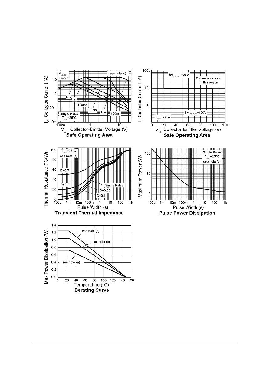
Absolute maximum ratings
NOTES:
(a) For a device surface mounted on 15mm x 15mm x 1.6mm FR4 PCB with high coverage of single sided 1oz copper, in
still air conditions.
(b) Mounted on 25mm x 25mm x 1.6mm FR4 PCB with a high coverage of single sided 2 oz copper in still air conditions.
(c) Mounted on 50mm x 50mm x 1.6mm FR4 PCB with a high coverage of single sided 2 oz copper in still air conditions.
(d) As (c) above measured at t<5secs.
Parameter
Symbol
Limit
Unit
Collector-base voltage
V
CBO
100
V
Collector-emitter voltage (forward blocking)
V
CEX
100
V
Collector-emitter voltage
V
CEO
20
V
Emitter-collector voltage (reverse blocking)
V
ECO
5
V
Emitter-base voltage
V
EBO
7
V
Continuous collector current
(c)
I
C
4.5
A
Peak pulse current
I
CM
15
A
Power dissipation at T
A
=25∞C
(a)
Linear Derating Factor
P
D
0.73
5.84
W
mW/∞C
Power dissipation at T
A
=25∞C
(b)
Linear derating factor
P
D
1.05
8.4
W
mW/∞C
Power dissipation at T
A
=25∞C
(c)
Linear derating factor
P
D
1.25
9.6
W
mW/∞C
Power dissipation at T
A
=25∞C
(d)
Linear derating factor
P
D
1.81
14.5
W
mW/∞C
Operating and storage temperature range
T
j
, T
stg
- 55 to 150
∞C
Thermal resistance
Parameter
Symbol
Limit
Unit
Junction to ambient
(a)
R
JA
171
∞C/W
Junction to ambient
(b)
R
JA
119
∞C/W
Junction to ambient
(c)
R
JA
100
∞C/W
Junction to ambient
(d)
R
JA
69
∞C/W

ZXTN25020DFH
Issue 1 - February 2006
4
www.zetex.com
© Zetex Semiconductors plc 2006
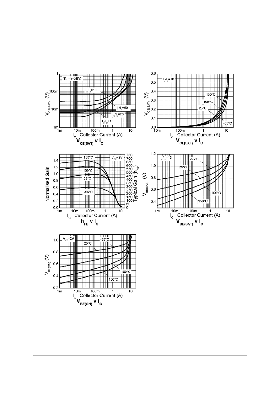
Electrical characteristics (at T
AMB
= 25∞C unless otherwise stated)
Parameter
Symbol
Min.
Typ.
Max.
Unit Conditions
Collector base breakdown voltage BV
CBO
100
125
V
I
C
= 100 A
Collector emitter breakdown
voltage (forward blocking)
BV
CEX
100
120
I
C
= 100 A, R
BE
< 1k or
-1V < V
BE
< 0.25V
Collector emitter breakdown
voltage (base open)
BV
CEO
20
35
V
I
C
= 10mA
(*)
NOTES:
(*) Measured under pulsed conditions. Pulse width
300 s; duty cycle
2%.
Emitter-collector breakdown
voltage (reverse blocking)
BV
ECX
6
8
V
I
E
= 100 A, R
BC
< 1k or
0.25V > V
BC
> -0.25V
Emitter-collector breakdown
voltage (base open)
BV
ECO
5
6
V
I
E
= 100mA,
Emitter base breakdown voltage BV
EBO
7
8.3
V
I
E
= 100mA
Collector cut-off current
I
CBO
<1
50
20
nA
A
V
CB
= 80V
V
CB
= 80V, T
AMB
= 100∞C
Collector emitter cut-off current
I
CEX
-
100
nA
V
CE
= 80V; R
BE
< 1k or
-1V < V
BE
< 0.25V
Emitter cut-off current
I
EBO
<1
50
nA
V
EB
= 5.6V
Collector emitter saturation
voltage
V
CE(sat)
35
43
mV
I
C
= 1A, I
B
= 100mA
(*)
55
70
mV
I
C
= 1A, I
B
= 20mA
(*)
90
110
mV
I
C
= 2A, I
B
= 40mA
(*)
125
170
mV
I
C
= 2A, I
B
= 20mA
(*)
125
150
mV
I
C
= 4,5A, I
B
= 450mA
(*)
205
265
mV
I
C
= 4.5A, I
B
= 90mA
(*)
Base emitter saturation voltage
V
BE(sat)
900
1000
mV
I
C
= 4.5A, I
B
= 90mA
(*)
Base emitter turn-on voltage
V
BE(on)
820
900
mV
I
C
= 4.5A, V
CE
= 2V
(*)
Static forward current transfer
ratio
h
FE
300
450
900
I
C
= 10mA, V
CE
= 2V
(*)
250
380
I
C
= 2A, V
CE
= 2V
(*)
120
170
I
C
= 4.5A, V
CE
= 2V
(*)
15
I
C
= 15A, V
CE
= 2V
(*)
Transition frequency
f
T
215
MHz I
C
= 50mA, V
CE
= 10V
f
= 100MHz
Output capacitance
C
OBO
16.5
pF
V
CB
= 10V, f
= 1MHz
(*)
Turn-on time
t
(on)
140
ns
V
CC
= 10V. I
C
= 1A,
I
B1
= I
B2
= 10mA.
Turn-off time
t
(off)
425
ns