 | –≠–ª–µ–∫—Ç—Ä–æ–Ω–Ω—ã–π –∫–æ–º–ø–æ–Ω–µ–Ω—Ç: ZXMP6A13F | –°–∫–∞—á–∞—Ç—å:  PDF PDF  ZIP ZIP |
SUMMARY
V
(BR)DSS
= -60V; R
DS(ON)
= 0.400
I
D
=-1.1A
DESCRIPTION
This new generation of trench MOSFETs from Zetex utilizes a unique structure that
combines the benefits of low on-resistance with fast switching speed. This makes
them ideal for high efficiency, low voltage, power management applications.
FEATURES
∑
Low on-resistance
∑
Fast switching speed
∑
Low threshold
∑
Low gate drive
∑
Low profile SOIC package
APPLICATIONS
∑
DC - DC converters
∑
Power management functions
∑
Relay and solenoid driving
∑
Motor control
DEVICE MARKING
∑
7P6
ZXMP6A13F
ISSUE 2 - JULY 2004
1
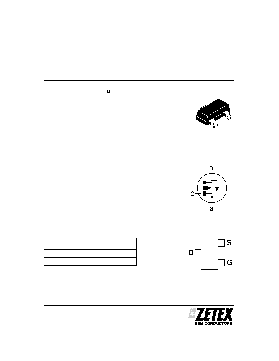
60V P-CHANNEL ENHANCEMENT MODE MOSFET
DEVICE
REEL
SIZE
TAPE
WIDTH
QUANTITY
PER REEL
ZXMP6A13FTA
7"
8mm
3000 units
ZXMP6A13FTC
13"
8mm
10000 units
ORDERING INFORMATION
SOT23
Top View
PINOUT

ZXMP6A13F
ISSUE 2 - JULY 2004
2
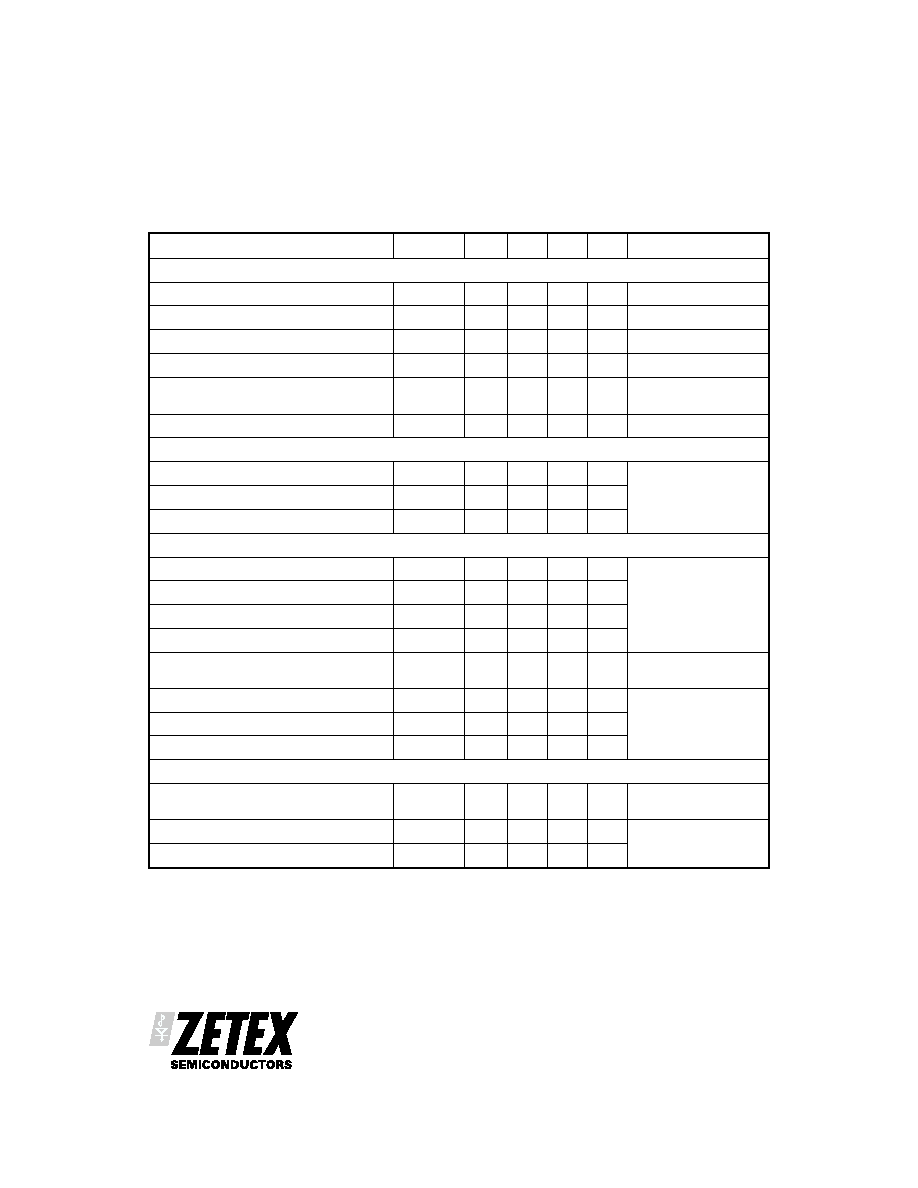
PARAMETER
SYMBOL
VALUE
UNIT
Junction to Ambient
(a)
R
JA
200
∞C/W
Junction to Ambient
(b)
R
JA
155
∞C/W
NOTES
(a) For a device surface mounted on 25mm x 25mm FR4 PCB with high coverage of single sided 1oz copper, in still air conditions
(b) For a device surface mounted on FR4 PCB measured at t
5 secs.
(c) Repetitive rating 25mm x 25mm FR4 PCB, D=0.05 pulse width=10µs - pulse width limited by maximum junction temperature.
THERMAL RESISTANCE
PARAMETER
SYMBOL
LIMIT
UNIT
Drain-Source Voltage
V
DSS
-60
V
Gate Source Voltage
V
GS
20
V
Continuous Drain Current V
GS
=10V; T
A
=25∞C
(b)
V
GS
=10V; T
A
=70∞C
(b)
V
GS
=10V; T
A
=25∞C
(a)
I
D
-1.1
-0.8
-0.9
A
Pulsed Drain Current
(c)
I
DM
-4.0
A
Continuous Source Current (Body Diode)
(b)
I
S
-1.2
A
Pulsed Source Current (Body Diode)
(c)
I
SM
-4.0
A
Power Dissipation at T
A
=25∞C
(a)
Linear Derating Factor
P
D
625
5
mW
mW/∞C
Power Dissipation at T
A
=25∞C
(b)
Linear Derating Factor
P
D
806
6.5
mW
mW/∞C
Operating and Storage Temperature Range
T
j
:T
stg
-55 to +150
∞C
ABSOLUTE MAXIMUM RATINGS.
CHARACTERISTICS
ZXMP6A13F
ISSUE 2 - JULY 2004
3
ZXMP6A13F
ISSUE 2 - JULY 2004
4
PARAMETER
SYMBOL
MIN.
TYP.
MAX.
UNIT
CONDITIONS
STATIC
Drain-Source Breakdown Voltage
V
(BR)DSS
-60
V
I
D
=-250 A, V
GS
=0V
Zero Gate Voltage Drain Current
I
DSS
-1
A
V
DS
=-60V, V
GS
=0V
Gate-Body Leakage
I
GSS
100
nA
V
GS
=
20V, V
DS
=0V
Gate-Source Threshold Voltage
V
GS(th)
-1.0
V
I
D
=-250 A, V
DS
= V
GS
Static Drain-Source On-State Resistance
(1)
R
DS(on)
0.400
0.600
V
GS
=-10V, I
D
=-0.9A
V
GS
=-4.5V, I
D
=-0.8A
Forward Transconductance
(1)(3)
g
fs
1.8
S
V
DS
=-15V,I
D
=-0.9A
DYNAMIC
(3)
Input Capacitance
C
iss
233
pF
V
DS
=-30V, V
GS
=0V,
f=1MHz
Output Capacitance
C
oss
17.4
pF
Reverse Transfer Capacitance
C
rss
9.6
pF
SWITCHING
(2) (3)
Turn-On Delay Time
t
d(on)
1.6
ns
V
DD
=-30V, I
D
=-1A
R
G
6.0 , V
GS
=-10V
Rise Time
t
r
2.3
ns
Turn-Off Delay Time
t
d(off)
13
ns
Fall Time
t
f
5.8
ns
Gate Charge
Q
g
2.4
nC
V
DS
=-30V,V
GS
=-5V,
I
D
=-0.9A
Total Gate Charge
Q
g
5.1
nC
V
DS
=-30V,V
GS
=-10V,
I
D
=-0.9A
Gate-Source Charge
Q
gs
0.7
nC
Gate-Drain Charge
Q
gd
0.7
nC
SOURCE-DRAIN DIODE
Diode Forward Voltage
(1)
V
SD
-0.85
-0.95
V
T
J
=25∞C, I
S
=-0.8A,
V
GS
=0V
Reverse Recovery Time
(3)
t
rr
22.6
ns
T
J
=25∞C, I
F
=-0.9A,
di/dt= 100A/
µs
Reverse Recovery Charge
(3)
Q
rr
23.2
nC
ELECTRICAL CHARACTERISTICS (at T
A
= 25∞C unless otherwise stated)
NOTES:
(1) Measured under pulsed conditions. Width
=300µs. Duty cycle 2% .
(2) Switching characteristics are independent of operating junction temperature.
(3) For design aid only, not subject to production testing.
ZXMP6A13F
ISSUE 2 - JULY 2004
5
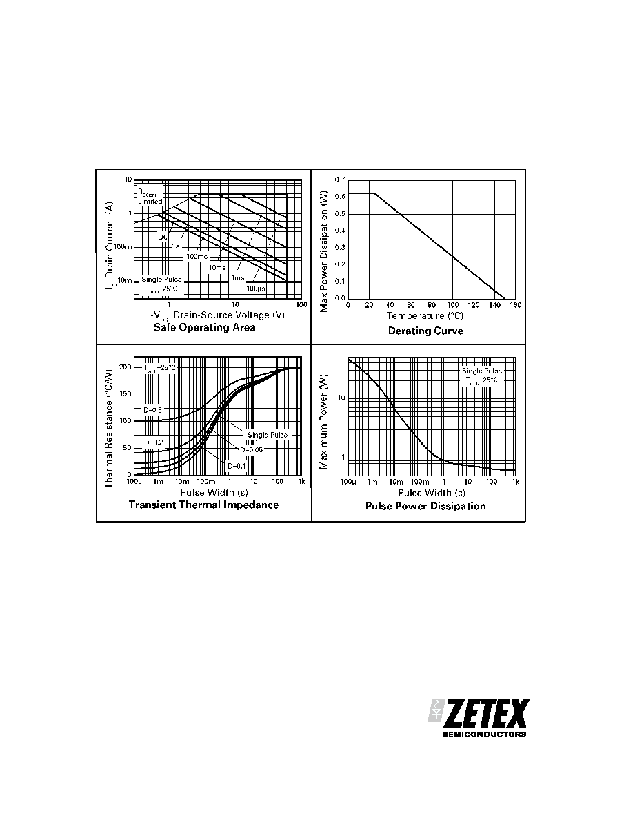
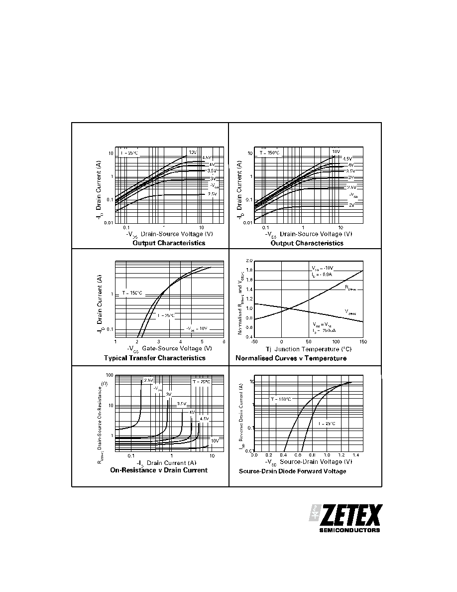
TYPICAL CHARACTERISTICS