
&55%%
P
RODUCT
S
PECIFICATION
<%
%/15 75% 7
0+8'45#.
5
'4+#.
%
10641..'4
('#674'5
∑
Two Independent 0-to-10-mbps Full-Duplex Channels,
each with Two Baud Rate Generators and One Digital
Phase-Locked Loop for Clock Recovery
∑
32-Byte Data FIFO's for each Receiver and Transmitter
∑
110-ns Bus Cycle Time, 16-Bit Data Bus Bandwidth
∑
Multi-Protocol Operation under Program Control with
Independent Mode Selection for Receiver and Transmit-
ter
∑
Async Mode with 1 to 8 Bits/Character, 1/16 to 2 Stop
Bits/Character in 1/16-Bit Increments; Programmable
Clock Factor; Break Detect and Generation; Odd, Even,
Mark, Space or no Parity and Framing Error Detection;
Supports One Address/Data Bit and MIL STD 1553B
Protocols
∑
Byte Oriented Synchronous Mode with One to Eight
Bits/Character; Programmable Idle Line Condition; Op-
tional Receive Sync Stripping; Optional Preamble
Transmission; 16- or 32-Bit CRC and Transmit-to-Re-
ceive Slaving (for X.21)
∑
Bisync Mode with 2- to 16-Bit Programmable Sync
Character; Programmable Idle Line Condition; Optional
Receive Sync Stripping; Optional Preamble Transmis-
sion; 16- or 32-Bit CRC
∑
Transparent Bisync Mode with EBCDIC or ASCII Char-
acter Code; Automatic CRC Handling; Programmable
Idle Line Condition; Optional Preamble Transmission;
Automatic Recognition of DLE, SYN, SOH, ITX, ETX,
ETB, EOT, ENQ and ITB
∑
External Character Sync Mode for Receive
∑
HDLC/SDLC Mode with Eight-Bit Address Compare;
Extended Address Field Option; 16- or 32-Bit CRC; Pro-
grammable Idle Line Condition; Optional Preamble
Transmission and Loop Mode
∑
DMA Interface with Separate Request and Acknowl-
edge for Each Receiver and Transmitter
∑
Channel Load Command for DMA Controlled Initializa-
tion
∑
Flexible Bus Interface for Direct Connection to Most
Microprocessors; User Programmable for 8 or 16 Bits
Wide. Directly Supports 680X0 Family or 8X86 Family
Bus Interfaces
∑
Low Power CMOS
∑
68-Pin PLCC/100-Pin VQFP Packages
)'0'4#. &'5%4+26+10
The Z16C30 USCTM Universal Serial Controller is a dual-
channel multi-protocol data communications peripheral de-
signed for use with any conventional multiplexed or non-
multiplexed bus. The USC functions as a serial-to-parallel,
parallel-to-serial converter/controller and may be software
configured to satisfy a wide variety of serial communica-
tions applications. The device contains a variety of new, so-
phisticated internal functions including two baud rate gen-
erators per channel, one digital phase-locked loop per
channel, character counters for both receive and transmit in
each channel and 32-byte data FIFO's for each receiver and
transmitter (Figure 1).
ZiLOG now offers a high speed version of the USC with
improved bus bandwidth. CPU bus accesses have been
shortened from 160 ns per access to 110 ns per access. The
USC has a transmit and receive clock range of up to 10 MHz

<%
%/15 75% 7PKXGTUCN 5GTKCN %QPVTQNNGT
ZiLOG
&55%%
)'0'4#. &'5%4+26+10
%QPVKPWGF
(20 MHz when using the DPLL, BRG, or CTR) and data
transfer rates as high as 10 Mbits/sec full duplex.
The USC handles asynchronous formats, synchronous
byte-oriented formats such as BISYNC and synchronous
bit-oriented formats such as HDLC. This device supports
virtually any serial data transfer application.
The device can generate and check CRC in any synchronous
mode and can be programmed to check data integrity in var-
ious modes. The USC also has facilities for modem controls
in both channels. In applications where these controls are
not needed, the modem controls may be used for general-
purpose I/O. The same is true for most of the other pins in
each channel.
Interrupts are supported with a daisy-chain hierarchy, with
the two channels having completely separate interrupt
structures.
High-speed data transfers through DMA are supported by
a Request/Acknowledge signal pair for each receiver and
transmitter. The device supports automatic status transfer
through DMA and also allows device initialization under
DMA control.
0QVG When written to, all reserved bits must be programmed
to 0.
To aid the designer in efficiently programming the USC,
support tools are available. The Technical Manual describes
in detail all features presented in this Product Specification
and gives programming sequence hints. The Programmer's
Assistant is a MS-DOS disk-based programming initializa-
tion tool to be used in conjunction with the Technical Man-
ual. There are also available assorted application notes and
development boards to assist the designer in the hard-
ware/software development.
All Signals with an overline, are active Low. For example:
B/W, in which WORD is active Low, and B/W, in which
BYTE is active Low.
Power connections follow these conventional descriptions:
%QPPGEVKQP
%KTEWKV
&GXKEG
2QYGT
8
77
8
88
)TQWPF
)0&
8
SS

<%
ZiLOG
%/15 75% 7PKXGTUCN 5GTKCN %QPVTQNNGT
&55%%
(KIWTG <% $NQEM &KCITCO
6Q 1VJGT %JCPPGN
4GEGKXG
4GEGKXG
(+(1
+PVGTTWRV
%QPVTQN
%JCPPGN
%QPVTQN
6TCPUOKV
(+(1
6TCPUOKV
&/#
+
1
&C
VC
$
W
H
H
G
T
%27
D[VG
%QPVTQN
&/#
D[VG
%QPVTQN
4GEGKXG &CVC
4GEGKXGT
4GEGKXG
6TCPUOKV
%NQEMU
6TCPUOKVVGT
6TCPUOKV &CVC
%NQEM /7:
&2..
%QWPVGTU
$4)
$4)
+1 CPF
&GXKEG
5VCVWU

<%
%/15 75% 7PKXGTUCN 5GTKCN %QPVTQNNGT
ZiLOG
&55%%
PIN DESCRIPTION
(KIWTG <% 2KP (WPEVKQPU
#&
#&
#&
#&
#&
#&
#&
#&
#&
#&
#&
#&
#&
#&
#&
#&
#5
&5
4&
94
%5
#$
&%
49
2+6#%-
5+6#%-
9#+64&;
8
55
8
55
8
55
8
55
8
55
8
55
8
55
6Z&#
4Z&#
6Z%#
4Z%#
%65#
&%&#
4Z4'3#
4Z#%-#
6Z4'3#
6Z#%-#
+06#
+'+#
+'1#
6Z&$
4Z&$
5GTKCN
&CVC
%JCPPGN
%NQEMU
%JCPPGN
+1
%JCPPGN
&/#
+PVGTHCEG
4GUGV
&GXKEG
6Z%$
4Z%$
%65$
&%&$
4Z4'3$
4Z#%-$
6Z4'3$
6Z#%-$
+06$
+'+$
+'1$
4'5'6
8
&&
8
&&
8
&&
8
&&
8
&&
8
&&
8
&&
%JCPPGN
+PVGTTWRV
+PVGTHCEG
)TQWPF
+PVGTTWRV
%QPVTQN
$WU
6KOKPI
#FFTGUU
&CVC
$WU
5GTKCN
&CVC
%JCPPGN
%NQEMU
%JCPPGN
+1
%JCPPGN
&/#
+PVGTHCEG
%JCPPGN
+PVGTTWRV
+PVGTHCEG
2QYGT

<%
ZiLOG
%/15 75% 7PKXGTUCN 5GTKCN %QPVTQNNGT
&55%%
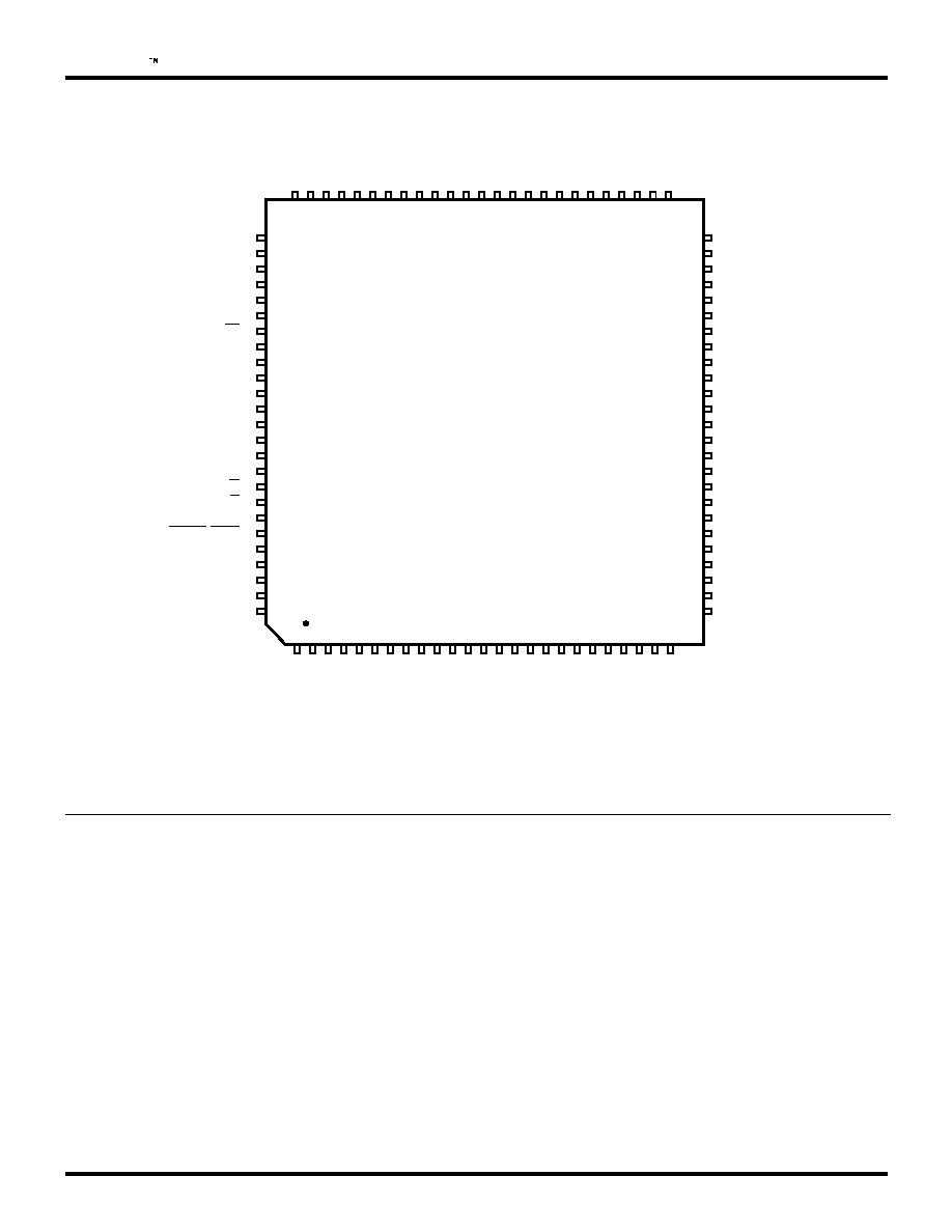
(KIWTG <% 2KP 2.%% 2KP #UUKIPOGPVU
60
44
10
26
4Z#%-#
+06#
+'+#
+'1#
)0&
8
%%
#&
#&
#&
#&
#&
#&
#&
#&
)0&
8
%%
4:4'3#
TXACKA
WAI
T
/
4&;
SIT
A
CK
A/
$
D/
%
CS
RESET
V
CC
V
CC
V
CC
AS
DS
RD
WR
R/
9
PIT
A
CK
TXACKB
2KP 2.%%
4:#%-$
+06$
+'+$
+'1$
)0&
8
%%
#&
#&
#&
#&
#&
#&
#&
#&
)0&
8
%%
4:4'3$
TX
R
E
Q
A
RXCA
RXDA
DCDA
TXCA
TXDA
CTSA
GN
D
GN
D
GN
D
CTSB
TXDB
TXCB
DCDB
RXDB
RXCB
TX
R
E
Q
B
<%
%/15 75% 7PKXGTUCN 5GTKCN %QPVTQNNGT
ZiLOG
&55%%
The Z16C30 contains 13 pins per channel for channel I/O,
16 pins for address and data, 12 pins for CPU handshake
and 14 pins for power and ground.
Three separate bus interface types are available for the de-
vice. The Bus Configuration Register (BCR) and external
connections to the AD bus control selection of the bus type.
A 16-bit bus is selected by setting BCR bit 2 to a 1. The 8-
bit bus is selected by setting BCR bit 2 to 0 and tying
AD15≠AD8 to V
SS
.
The 8-bit bus with separate address is selected by setting
BCR bit 2 to 0 and, during the BCR write, forcing AD15
to a 1 and forcing AD14≠AD8 to 0.
The multiplexed bus is selected for the USC if there is an
Address Strobe prior to or during the transaction which
writes the BCR. If no Address Strobe is present prior to or
during the transaction which writes the BCR, a nonmulti-
plexed bus is selected (see Figure 29).
(KIWTG 2KP 83(2 2KP #UUKIPOGPVU
50
49
48
47
46
45
44
43
42
41
40
39
38
37
36
35
34
33
32
31
30
29
28
27
26
76
77
78
79
80
81
82
83
84
85
86
87
88
89
90
91
92
93
94
95
96
97
98
99
100
0%
0%
0%
0%
6:#%-$
2+6#%-
49
94
4&
&5
#5
8
%%
8
%%
8
%%
4'5'6
%5
&%
#$
5+6#%-
9#+64&;
6:#%-#
0%
0%
0%
0%
0%
0%
0%
0%
6:4'3$
4:%$
4:&$
&%&$
6:%$
6:&$
%65$
)0&
)0&
)0&
%65#
6:&#
6:%#
&%&#
4:&#
4:%#
6:4'3#
0%
0%
0%
0%
4:
#
%
-
#
+0
6
#
+'
+#
+'
1
#
)0
&
8
%
%
#&
0% 0% 0% 0%
#&
#&
#&
0% 0% 0% 0%
#&
#&
#&
#&
)0
&
8
%
%
4:4'3#
4:
#
%
-
$
+06$ +'
+$
+'
1
$
)0
&
8
%
%
#&
0% 0% 0% 0% #&
#&
#&
0% 0% 0% 0% #&
#&
#&
#&
)0
&
8
%
%
4
:
4'3$
2KP 83(2

<%
ZiLOG
%/15 75% 7PKXGTUCN 5GTKCN %QPVTQNNGT
&55%%
2+0 (70%6+105
4'5'6 4GUGV
KPRWV CEVKXG .QY
This signal resets the
device to a known state. The first write to the USC after a
reset accesses the BCR to select additional bus options for
the device.
#5 #FFTGUU 5VTQDG
KPRWV CEVKXG .QY
This signal is
used in the multiplexed bus modes to latch the address on
the AD lines. The AS signal is not used in the nonmulti-
plexed bus modes and should be tied to V
DD
.
&5 &CVC 5VTQDG
KPRWV CEVKXG .QY
This signal strobes
data out of the device during a read and may strobe an in-
terrupt vector out of the device during an interrupt acknowl-
edge cycle. DS also strobes data into the device on the state
of R/W.
4& 4GCF 5VTQDG
KPRWV CEVKXG .QY
This signal strobes
data out of the device during a read and may strobe an in-
terrupt vector out of the device during an interrupt acknowl-
edge cycle.
94 9TKVG 5VTQDG
KPRWV CEVKXG .QY
T h i s s i g n a l
strobes data into the device during a write.
49 4GCF9TKVG
KPRWV
This signal determines the direc-
tion of data transfer for a read or write cycle in conjunction
with DS.
%5 %JKR 5GNGEV
KPRWV CEVKXG .QY
This signal selects
the device for access and must be asserted for read and write
cycles, but is ignored during interrupt acknowledge and fly-
by DMA transfers. In the case of a multiplexed bus inter-
face, CS is latched by the rising edge of AS.
#$ %JCPPGN #%JCPPGN $ 5GNGEV
KPRWV
This signal se-
lects between the two channels in the device. High selects
channel A and Low selects channel B. This signal is sam-
pled and the result is latched during the BCR (Bus Config-
uration Register) write. It programs the sense of the
WAIT/RDY signal appropriate for different bus interfaces.
&% &CVC%QPVTQN 5GNGEV
KPRWV
This signal, when High,
provides for direct access to the RDR and TDR. In the case
of a multiplexed bus interface, D/
%
High overrides the ad-
dress provided to the device.
5+6#%- 5VCVWU +PVGTTWRV #EMPQYNGFIG
KPRWV CEVKXG
.QY
This signal is a status signal that indicates that an in-
terrupt acknowledge cycle is in progress. The device is ca-
pable of returning an interrupt vector that may be encoded
with the type of interrupt pending during this acknowledge
cycle. This signal is compatible with 680X0 family micro-
processors.
2+6#%- 2WNUGF +PVGTTWRV #EMPQYNGFIG
KPRWV CEVKXG
.QY
This signal is a strobe signal that indicates that an in-
terrupt acknowledge cycle is in progress. The device is ca-
pable of returning an interrupt vector that may be encoded
with the type of interrupt pending during this acknowledge
cycle. PITACK may be programmed to accept a single pulse
or double pulse acknowledge type. This programming is
done in the BCR. With the double pulse type selected, the
first PITACK is recognized but no action takes place. The
interrupt vector is returned on the second pulse if the no vec-
tor option is not selected. The double pulse type is compat-
ible with 8X86 family microprocessors.
9#+64&; 9CKV&CVC 4GCF[
QWVRWV CEVKXG .QY
T h i s
signal serves to indicate when the data is available during
a read cycle, when the device is ready to receive data during
a write cycle, and when a valid vector is available during
an interrupt acknowledge cycle. It may be programmed to
function either as a Wait signal or a Ready signal using the
state of the A/
$
pin during the BCR write. When A/B is High
during the BCR write, this signal functions as a wait output
and thus supports the READY function of 8X86 family mi-
croprocessors. When A/B is Low during the BCR write, this
signal functions as a ready output and thus supports the
DTACK function of 680X0 family microprocessors.
#& #& #FFTGUU&CVC $WU
DKFKTGEVKQPCN CEVKXG
*KIJ VTKUVCVG
The AD signals carry addresses to, and
data to and from, the device. When the 16-bit nonmulti-
plexed bus is selected, AD15≠AD0 carry data to and from
the device. Addresses are provided using a pointer within
the device that is loaded with the desired register address.
When selecting the 8-bit nonmultiplexed bus (without sep-
arate address) only AD7≠AD0 are used to transfer data. The
pointer is used for addressing, with AD15≠AD8 unused.
When selecting the 8-bit nonmultiplexed bus (with separate
address), AD7≠AD0 are used to transfer data with
AD15≠AD8 used as address bus. When the 16-bit multi-
plexed bus is selected, addresses are latched from
AD7≠AD0 and data transfers are sixteen bits wide. When
selecting the 8-bit multiplexed bus (without separate ad-
dress) only AD7≠AD0 are used to transfer addresses and
data, with AD15≠AD8 unused. When the 8-bit multiplexed
bus with separate address is selected, only AD7≠AD0 are
used to transfer data, while AD15≠AD8 are used as an ad-
dress bus.
+06# +06$ +PVGTTWRV 4GSWGUV
QWVRWVU CEVKXG .QY
T h e s e
signals indicate that the channel has an interrupt condition
pending and is requesting service. These outputs are NOT
open-drain.

<%
%/15 75% 7PKXGTUCN 5GTKCN %QPVTQNNGT
ZiLOG
&55%%
+'+# +'+$ +PVGTTWRV 'PCDNG +P
KPRWVU CEVKXG *KIJ
T h e
IEI signal for each channel is used with the accompanying
IEO signal to form an interrupt daisy chain. An active IEI
indicates that no device having higher priority is requesting
or servicing an interrupt.
+'1# +'1$ +PVGTTWRV 'PCDNG 1WV
QWVRWVU CEVKXG *KIJ
The IEO signal for each channel is used with the accompa-
nying IEI signal to form an interrupt daisy chain. IEO is Low
if IEI is Low, an interrupt is under service in the channel,
or an interrupt is pending during an interrupt acknowledge
cycle.
6Z#%-# 6Z#%-$ 6TCPUOKV #EMPQYNGFIG
KPRWVU QT
QWVRWVU CEVKXG .QY
The primary function of these sig-
nals is to perform fly-by DMA transfers to the transmit
FIFOs. They may also be used as bit inputs or outputs.
4Z#%-# 4Z#%-$ 4GEGKXG #EMPQYNGFIG
KPRWVU QT
QWVRWVU CEVKXG .QY
The primary function of these sig-
nals is to perform fly-by DMA transfers from the receive
FIFOs. They may also be used as bit inputs or outputs.
6Z&# 6Z&$ 6TCPUOKV &CVC
QWVRWVU CEVKXG *KIJ VTK
UVCVG
These signals carry the serial transmit data for each
channel.
4Z&# 4Z&$ 4GEGKXG &CVC
KPRWVU CEVKXG *KIJ
These
signals carry the serial receive data for each channel.
6Z%# 6Z%$ 6TCPUOKV %NQEM
KPRWVU QT QWVRWVU CEVKXG
.QY
These signals are used as clock inputs for any of the
functional blocks within the device. They may also be used
as outputs for various transmitter signals or internal clock
signals.
4Z%# 4Z%$ 4GEGKXG %NQEM
KPRWVU QT QWVRWVU CEVKXG
.QY
These signals are used as clock inputs for any of the
functional blocks within the device. They may also be used
as outputs for various receiver signals or internal clock sig-
nals.
6Z4'3# 6Z4'3$ 6TCPUOKV 4GSWGUV
KPRWVU QT QWVRWVU
CEVKXG .QY
The primary function of these signals is to re-
quest DMA transfers to the transmit FIFOs. They may also
be used as simple inputs or outputs.
4Z4'3# 4Z4'3$ 4GEGKXG 4GSWGUV
KPRWVU QT QWVRWVU
CEVKXG .QY
The primary function of these signals is to re-
quest DMA transfers from the receive FIFOs. They may
also be used as simple inputs or outputs.
%65# %65$ %NGCT 6Q 5GPF
KPRWVU QT QWVRWVU CEVKXG
.QY
These signals are used as enables for the respective
transmitters. They may also be programmed to generate in-
terrupts on either transition or used as simple inputs or out-
puts.
&%&# &%&$ &CVC %CTTKGT &GVGEV
KPRWVU QT QWVRWVU
CEVKXG .QY
These signals are used as enables for the re-
spective receivers. They may also be programmed to gen-
erate interrupts on either transition or used as simple inputs
or outputs.
<%
ZiLOG
%/15 75% 7PKXGTUCN 5GTKCN %QPVTQNNGT
&55%%
#$51.76' /#:+/7/ 4#6+0)5
Stresses greater than those listed under Absolute Maximum
Ratings may cause permanent damage to the device. This
is a stress rating only; operation of the device at any con-
dition above those indicated in the operational sections of
these specifications is not implied. Exposure to absolute
maximum rating conditions for extended periods may affect
device reliability.
56#0& 6'56 %10&+6+105
The DC Characteristics and Capacitance section below ap-
ply for the following standard test conditions, unless oth-
erwise noted. All voltages are referenced to GND. Positive
current flows into the referenced pin (Figure 5). Standard
conditions are as follows:
∑
+4.5 V < V
CC
< +5.5 V
∑
GND = 0 V
∑
T
A
as specified in Ordering Information
5[ODQN
&GUETKRVKQP
/KP
/CZ
7PKVU
8
77
5WRRN[ 8QNVCIG
�
8
6
STA
5VQTCIG 6GOR
u
u
%
6
5
1RGT #ODKGPV
6GOR
%
2QYGT &KUUKRCVKQP
9
0QVGU
�8QNVCIG QP CNN RKPU YKVJ TGURGEV VQ )0&
5GG 1TFGTKPI +PHQTOCVKQP
(KIWTG 6GUV .QCF &KCITCO
From Pin
50 pF
C
L
I
OL
I
OH
V
OL
max +V
OH
min
2

<%
%/15 75% 7PKXGTUCN 5GTKCN %QPVTQNNGT
ZiLOG
&55%%
CAPACITANCE
/+5%'..#0'175
6TCPUKUVQT %QWPV
6'/2'4#674' 4#6+0)5
Standard = 0∞C to ±70∞C
Extended = ≠40∞C to +85∞C
&% %*#4#%6'4+56+%5
<%
5[ODQN
2CTCOGVGT
/KP
/CZ
7PKV
%QPFKVKQP
%
CH
+PRWV %CRCEKVCPEG
R(
7POGCUWTGF RKPU
%
IUT
1WVRWV %CRCEKVCPEG
R(
TGVWTPGF VQ )TQWPF
%+1
$KFKTGEVKQPCN %CRCEKVCPEG
R(
0QVG
f = 1 MHz over specified temperature range.
5[ODQN
2CTCOGVGT
/KP
6[R
/CZ
7PKV
%QPFKVKQP
8
CB
+PRWV *KIJ 8QNVCIG
8
77
8
8
CF
+PRWV .QY 8QNVCIG
8
8
IB
1WVRWV *KIJ 8QNVCIG
8
+
IB¬
O#
8
IB
1WVRWV *KIJ 8QNVCIG
8
77
8
+
IB
z#
8
IF
1WVRWV .QY 8QNVCIG
8
+
IF
O#
+
CF
+PRWV .GCMCIG
v
z#
8
CH
8
+
IF
1WVRWV .GCMCIG
v
z#
8
IUT
8
+
77x
8
77
5WRRN[ %WTTGPV
O#
8
77
8 8
CB
8 8
CF
8
0QVG
V
CC
= 5V ±10% unless otherwise specified, over specified temperature range.

<%
ZiLOG
%/15 75% 7PKXGTUCN 5GTKCN %QPVTQNNGT
&55%%
#% %*#4#%6'4+56+%5
<%
6CDNG #% %JCTCEVGTKUVKEU
0Q
5[ODQN
2CTCOGVGT
/KP
/CZ
7PKVU
0QVG
6E[E
$WU %[ENG 6KOG
PU
6Y#5N
#5 .QY 9KFVJ
PU
6Y#5J
#5 *KIJ 9KFVJ
PU
6Y&5N
&5 .QY 9KFVJ
PU
6Y&5J
&5 *KIJ 9KFVJ
PU
6F#5
&5
#5 4KUG VQ &5 (CNN &GNC[ 6KOG
PU
6F&5
#5
&5 4KUG VQ #5 (CNN &GNC[ 6KOG
PU
6F&5
&4C
&5 (CNN VQ &CVC #EVKXG &GNC[
PU
6F&5
&4X
&5 (CNN VQ &CVC 8CNKF &GNC[
PU
6F&5
&4P
&5 4KUG VQ &CVC 0QV 8CNKF &GNC[
PU
6F&5
&4\
&5 4KUG VQ &CVC (NQCV &GNC[
PU
6U%5
#5
%5 VQ #5 4KUG 5GVWR 6KOG
PU
6J%5
#5
%5 VQ #5 4KUG *QNF 6KOG
PU
6U#&&
#5
&KTGEV #FFTGUU VQ #5 4KUG 5GVWR 6KOG
PU
6J#&&
#5
&KTGEV #FFTGUU VQ #5 4KUG *QNF 6KOG
PU
6U5+#
#5
5+6#%- VQ #5 4KUG 5GVWR 6KOG
PU
6J5+#
#5
5+6#%- VQ #5 4KUG *QNF 6KOG
PU
6U#&
#5
#FFTGUU VQ #5 4KUG 5GVWR 6KOG
PU
6J#&
#5
#FFTGUU VQ #5 4KUG *QNF 6KOG
PU
6U49
&5
49 VQ &5 (CNN 5GVWR 6KOG
PU
6J49
&5
49 VQ &5 (CNN *QNF 6KOG
PU
6U&5H
443
&5 (CNN VQ 4Z4'3 +PCEVKXG &GNC[
PU
6F&5T
443
&5 4KUG VQ 4Z4'3 #EVKXG &GNC[
PU
6U&9
&5
9TKVG &CVC VQ &5 4KUG 5GVWR 6KOG
PU
6J&9
&5
9TKVG &CVC VQ &5 4KUG *QNF 6KOG
PU
6F&5H
643
&5 (CNN VQ 6Z4'3 +PCEVKXG &GNC[
PU
6F&5T
643
&5 4KUG VQ 6Z4'3 #EVKXG &GNC[
PU
6Y4&N
4& .QY 9KFVJ
PU
6Y4&J
4& *KIJ 9KFVJ
PU
6F#5
4&
#5 4KUG VQ 4& (CNN &GNC[ 6KOG
PU
6F4&
#5
4& 4KUG VQ #5 (CNN &GNC[ 6KOG
PU
6F4&
&4C
4& (CNN VQ &CVC #EVKXG &GNC[
PU
6F4&
&4X
4& (CNN VQ &CVC 8CNKF &GNC[
PU
6F4&
&4P
4& 4KUG VQ &CVC 0QV 8CNKF &GNC[
PU
6F4&
&4\
4& 4KUG VQ &CVC (NQCV &GNC[
PU
6F4&H
443
4& (CNN VQ 4Z4'3 +PCEVKXG &GNC[
PU
6F4&T
443
4& 4KUG VQ 4Z4'3 #EVKXG &GNC[
PU
6Y94N
94 .QY 9KFVJ
PU

<%
%/15 75% 7PKXGTUCN 5GTKCN %QPVTQNNGT
ZiLOG
&55%%
#% %*#4#%6'4+56+%5
%QPVKPWGF
6Y94J
94 *KIJ 9KFVJ
PU
6F#5
94
#5 4KUG VQ 94 (CNN &GNC[ 6KOG
PU
6F94
#5
94 4KUG VQ #5 (CNN &GNC[ 6KOG
PU
6U&9
94
9TKVG &CVC VQ 94 4KUG 5GVWR 6KOG
PU
6J&9
94
9TKVG &CVC VQ 94 4KUG *QNF 6KOG
PU
6F94H
643
94 (CNN VQ 6Z4'3 +PCEVKXG &GNC[
PU
6F94T
643
94 4KUG VQ 6Z4'3 #EVKXG &GNC[
PU
6U%5
&5
%5 VQ &5 (CNN 5GVWR 6KOG
PU
6J%5
&5
%5 VQ &5 (CNN *QNF 6KOG
PU
6U#&&
&5
&KTGEV #FFTGUU VQ &5 (CNN 5GVWR 6KOG
PU
6J#&&
&5
&KTGEV #FFTGUU VQ &5 (CNN *QNF 6KOG
PU
6U5+#
&5
5+6#%- VQ &5 (CNN 5GVWR 6KOG
PU
6J5+#
&5
5+6#%- VQ &5 (CNN *QNF 6KOG
PU
6U%5
4&
%5 VQ 4& (CNN 5GVWR 6KOG
PU
6J%5
4&
%5 VQ 4& (CNN *QNF 6KOG
PU
6U#&&
4&
&KTGEV #FFTGUU VQ 4& (CNN 5GVWR 6KOG
PU
6J#&&
4&
&KTGEV #FFTGUU VQ 4& (CNN *QNF 6KOG
PU
6U5+#
4&
5+6#%- VQ 4& (CNN 5GVWR 6KOG
PU
6J5+#
4&
5+6#%- VQ 4& (CNN *QNF 6KOG
PU
6U%5
94
%5 VQ 94 (CNN 5GVWR 6KOG
PU
6J%5
94
%5 VQ 94 (CNN *QNF 6KOG
PU
6U#&&
94
&KTGEV #FFTGUU VQ 94 (CNN 5GVWR 6KOG
PU
6J#&&
94
&KTGEV #FFTGUU VQ 94 (CNN *QNF 6KOG
PU
6U5+#
94
5+6#%- VQ 94 (CNN 5GVWR 6KOG
PU
6J5+#
94
5+6#%- VQ 94 (CNN *QNF 6KOG
PU
6Y4#-N
4Z#%- .QY 9KFVJ
PU
6Y4#-J
4Z#%- *KIJ 9KFVJ
PU
6F4#-
&4C
4Z#%- (CNN VQ &CVC #EVKXG &GNC[
PU
6F4#-
&4X
4Z#%- (CNN VQ &CVC 8CNKF &GNC[
PU
6F4#-
&4P
4Z#%- 4KUG VQ &CVC 0QV 8CNKF &GNC[
PU
6F4#-
&4\
4Z#%- 4KUG VQ &CVC (NQCV &GNC[
PU
6F4#-H
443
4Z#%- (CNN VQ 4Z4'3 +PCEVKXG &GNC[
PU
6F4#-T
443
4Z#%- 4KUG VQ 4Z4'3 #EVKXG &GNC[
PU
6Y6#-N
6Z#%- .QY 9KFVJ
PU
6Y6#-J
6Z#%- *KIJ 9KFVJ
PU
6U&9
6#-
9TKVG &CVC VQ 6Z#%- 4KUG 5GVWR 6KOG
PU
6J&9
6#-
9TKVG &CVC VQ 6Z#%- 4KUG *QNF 6KOG
PU
6F6#-H
643
6Z#%- (CNN VQ 6Z4'3 +PCEVKXG &GNC[
PU
6F6#-T
643
6Z#%- 4KUG VQ 6Z4'3 #EVKXG &GNC[
PU
6F&5H
4&;
&5 (CNN
+06#%- VQ 4&; (CNN &GNC[
PU
6CDNG #% %JCTCEVGTKUVKEU
%QPVKPWGF
0Q
5[ODQN
2CTCOGVGT
/KP
/CZ
7PKVU
0QVG

<%
ZiLOG
%/15 75% 7PKXGTUCN 5GTKCN %QPVTQNNGT
&55%%
6F4&;
&4X
4&; (CNN VQ &CVC 8CNKF &GNC[
PU
6F&5T
4&;
&5 4KUG VQ 4&; 4KUG &GNC[
PU
6U+'+
&5+
+'+ VQ &5 (CNN
+06#%- 5GVWR 6KOG
PU
6J+'+
&5+
+'+ VQ &5 4KUG
+06#%- *QNF 6KOG
PU
6F+'+
+'1
+'+ VQ +'1 &GNC[
PU
6F#5
+'1
#5 4KUG
+PVCEM VQ +'1 &GNC[
PU
6F&5+
+06
&5 (CNN
+06#%- VQ +06 +PCEVKXG &GNC[
PU
6F&5+
9T
&5 (CNN
+06#%- VQ 9#+6 4KUG &GNC[
PU
6F9
&4X
9#+6 4KUG VQ &CVC 8CNKF &GNC[
PU
6F4&H
4&;
4& (CNN
+06#%- VQ 4&; (CNN &GNC[
PU
6F4&T
4&;
4& 4KUG VQ 4&; 4KUG &GNC[
PU
6U+'+
4&+
+'+ VQ 4& (CNN
+06#%- 5GVWR 6KOG
PU
6J+'+
4&+
+'+ VQ 4& 4KUG
+06#%- *QNF 6KOG
PU
6F4&+
+06
4& (CNN
+06#%- VQ +06 +PCEVKXG &GNC[
PU
6F4&+
9H
4& (CNN
+06#%- VQ 9#+6 (CNN &GNC[
PU
6F4&+
9T
4& (CNN
+06#%- VQ 9#+6 4KUG &GNC[
PU
6Y2+#N
2+6#%- .QY 9KFVJ
PU
6Y2+#J
2+6#%- *KIJ 9KFVJ
PU
6F#5
2+#
#5 4KUG VQ 2+6#%- (CNN &GNC[ 6KOG
PU
6F2+#
#5
2+6#%- 4KUG VQ #5 (CNN &GNC[ 6KOG
PU
6F2+#
&4C
2+6#%- (CNN VQ &CVC #EVKXG &GNC[
PU
6F2+#
&4P
2+6#%- 4KUG VQ &CVC 0QV 8CNKF &GNC[
PU
6F2+#
&4\
2+6#%- 4KUG VQ &CVC (NQCV &GNC[
PU
6U+'+
2+#
+'+ VQ 2+6#%- (CNN 5GVWR 6KOG
PU
6J+'+
2+#
+'+ VQ 2+6#%- 4KUG *QNF 6KOG
PU
6F2+#
+'1
2+6#%- (CNN VQ +'1 &GNC[
PU
6F2+#
+06
2+6#%- (CNN VQ +06 +PCEVKXG &GNC[
PU
6F2+#H
4&;
2+6#%- (CNN VQ 4&; (CNN &GNC[
PU
6F2+#T
4&;
2+6#%- 4KUG VQ 4&; 4KUG &GNC[
PU
6F2+#
9H
2+6#%- (CNN VQ 9#+6 (CNN &GNC[
PU
6F2+#
9T
2+6#%- (CNN VQ 9#+6 4KUG &GNC[
PU
6F5+#
+06
5+6#%- (CNN VQ +'1 +PCEVKXG &GNC[
PU
6Y56$J
5VTQDG *KIJ 9KFVJ
PU
6Y4'5N
4'5'6 .QY 9KFVJ
PU
6Y4'5J
4'5'6 *KIJ 9KFVJ
PU
6FTGU
56$
4'5'6 4KUG VQ 56$ (CNN
PU
6F&5H
4&;
&5 (CNN VQ 4&; (CNN &GNC[
PU
6F94H
4&;
94 (CNN VQ 4&; (CNN &GNC[
PU
6F94T
4&;
94 4KUG VQ 4&; 4KUG &GNC[
PU
6F4&H
4&;
4& (CNN VQ 4&; (CNN &GNC[
PU
6F4#-H
4&;
4Z#%- (CNN VQ 4&; (CNN &GNC[
PU
6CDNG #% %JCTCEVGTKUVKEU
%QPVKPWGF
0Q
5[ODQN
2CTCOGVGT
/KP
/CZ
7PKVU
0QVG

<%
%/15 75% 7PKXGTUCN 5GTKCN %QPVTQNNGT
ZiLOG
&55%%
#% %*#4#%6'4+56+%5
%QPVKPWGF
6F4#-T
4&;
4Z#%- 4KUG VQ 4&; 4KUG &GNC[
PU
6F6#-H
4&;
6Z#%- (CNN VQ 4&; (CNN &GNC[
PU
6F6#-T
4&;
6Z#%- 4KUG VQ 4&; 4KUG &GNC[
PU
0QVGU
&KTGEV CFFTGUU KU CP[ QH #$ &% QT #& #& WUGF CU CP CFFTGUU DWU
6JG RCTCOGVGT CRRNKGU QPN[ YJGP #5 KU PQV RTGUGPV
5VTQDG
56$ KU CP[ QH &5 4& 94 2+6#%- 4Z#%- QT 6Z#%-
2CTCOGVGT CRRNKGU QPN[ KH TGCF GORVKGU VJG TGEGKXG (+(1
2CTCOGVGT CRRNKGU QPN[ KH YTKVG HKNNU VJG VTCPUOKV (+(1
(QT GZVGPFGF VGORGTCVWTG RCTV 6F&5+
9H OCZ PU
(QT GZVGPFGF VGORGTCVWTG RCTV 6F&5(
643 OCZ PU
6CDNG #% %JCTCEVGTKUVKEU
%QPVKPWGF
0Q
5[ODQN
2CTCOGVGT
/KP
/CZ
7PKVU
0QVG
<%
ZiLOG
%/15 75% 7PKXGTUCN 5GTKCN %QPVTQNNGT
&55%%
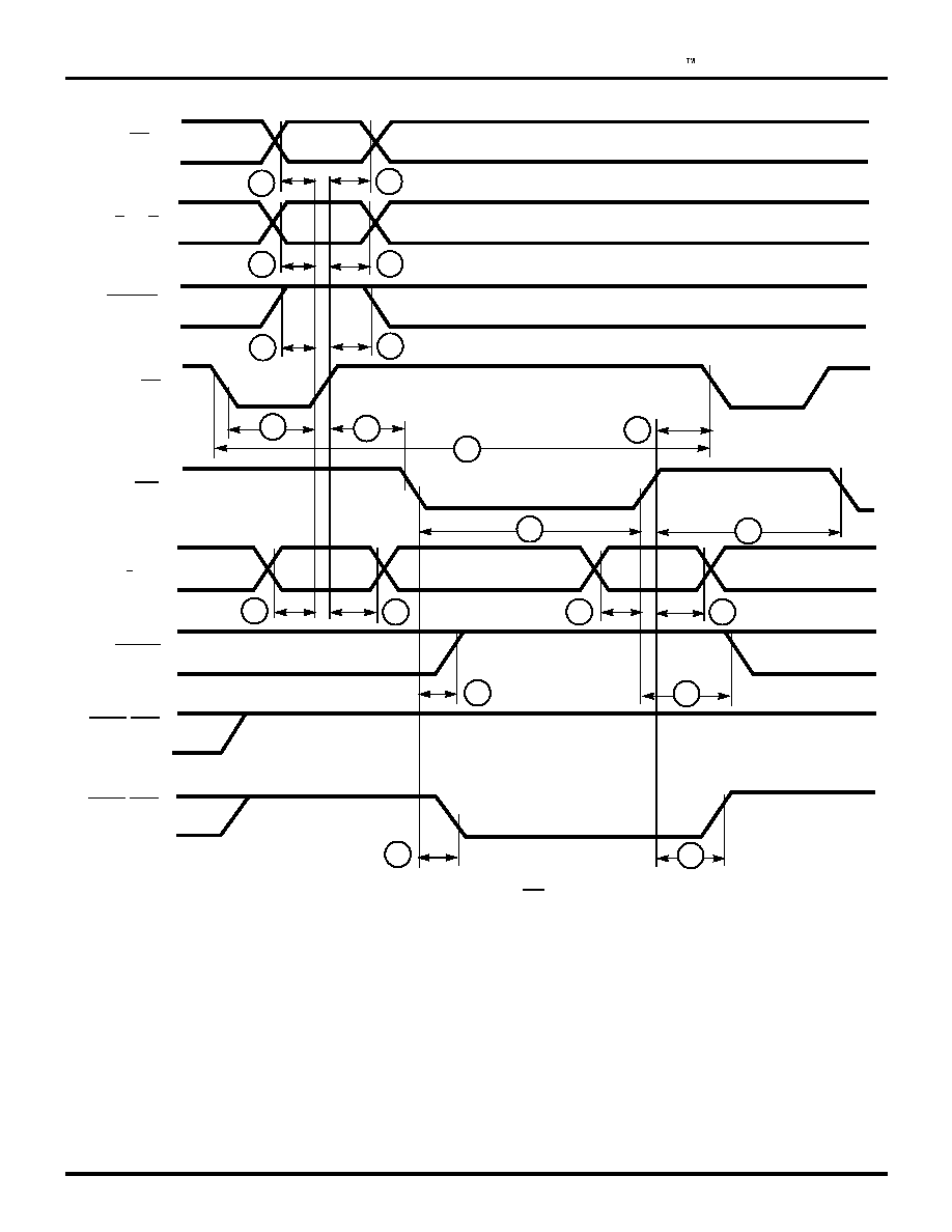
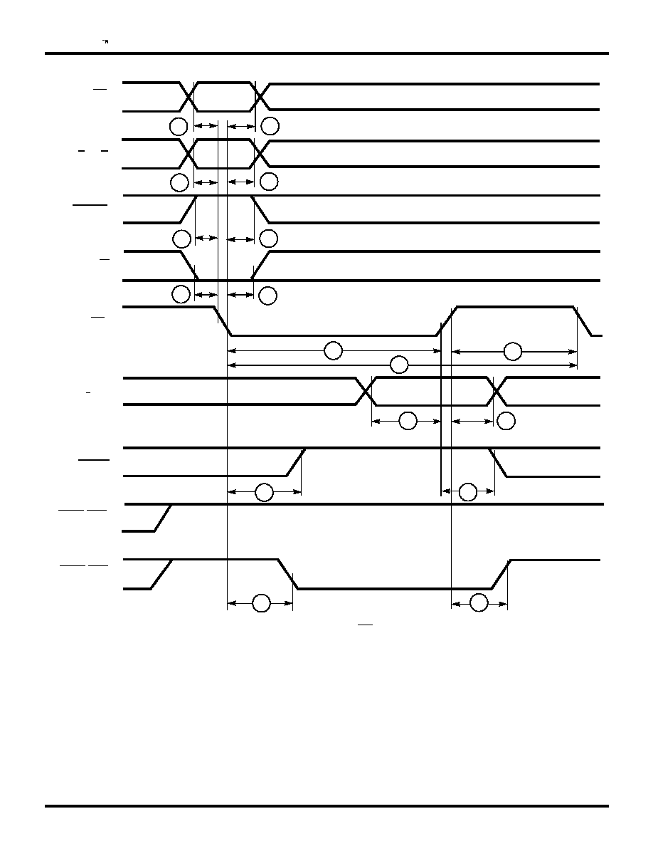
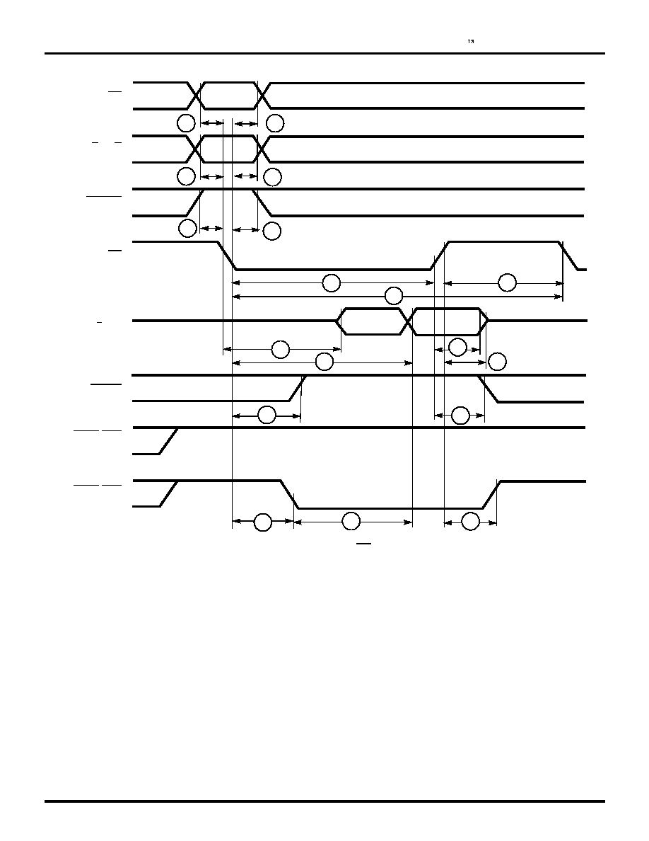
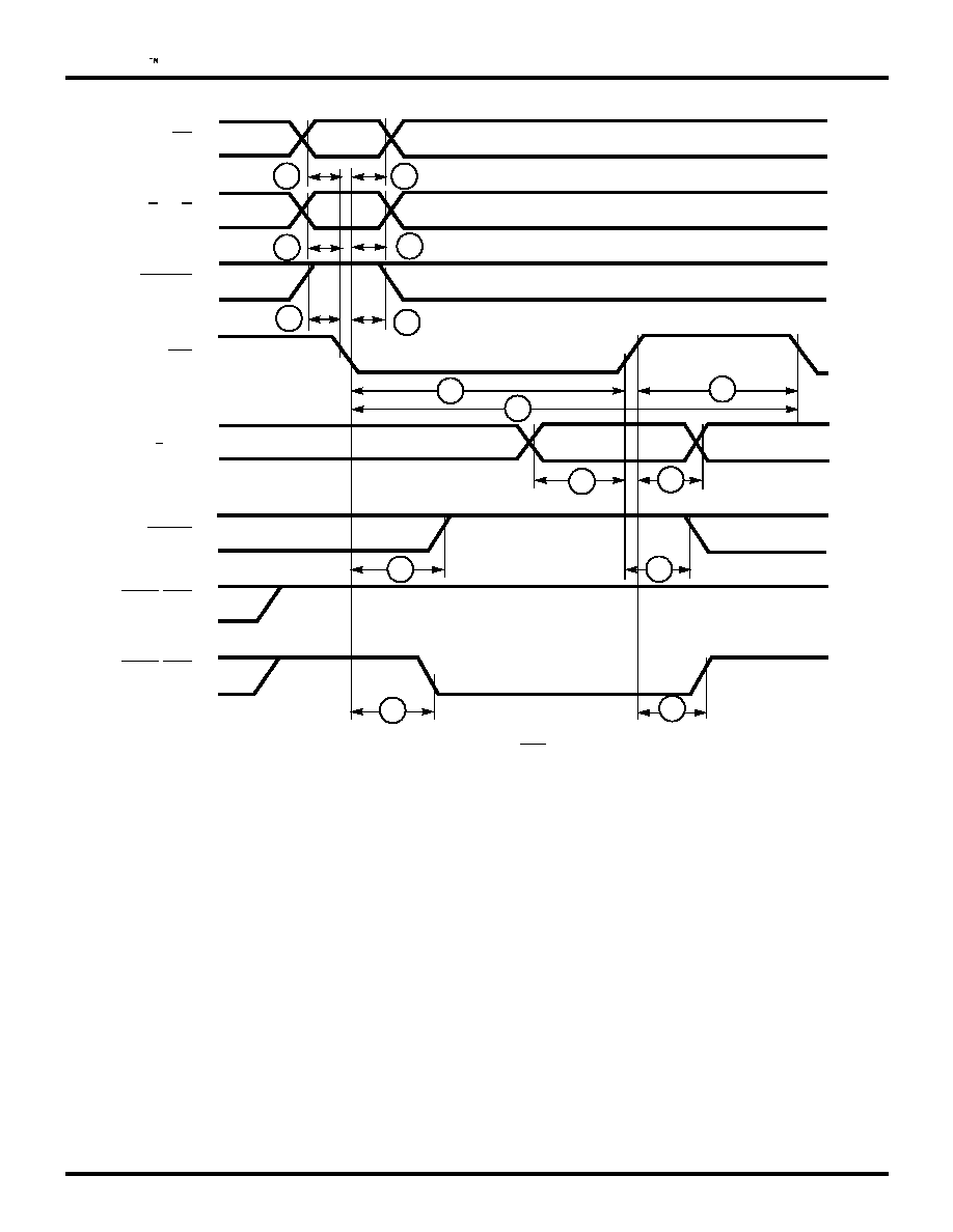
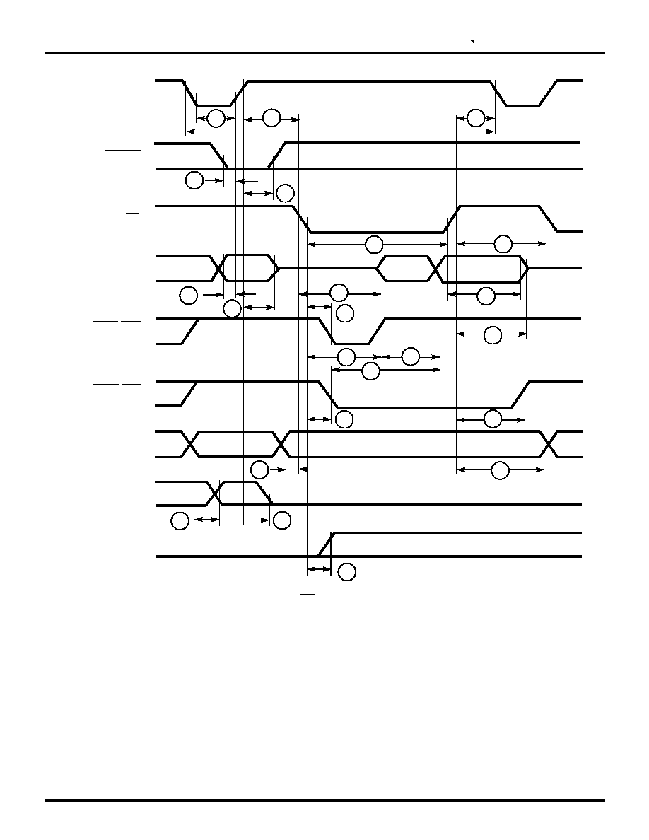
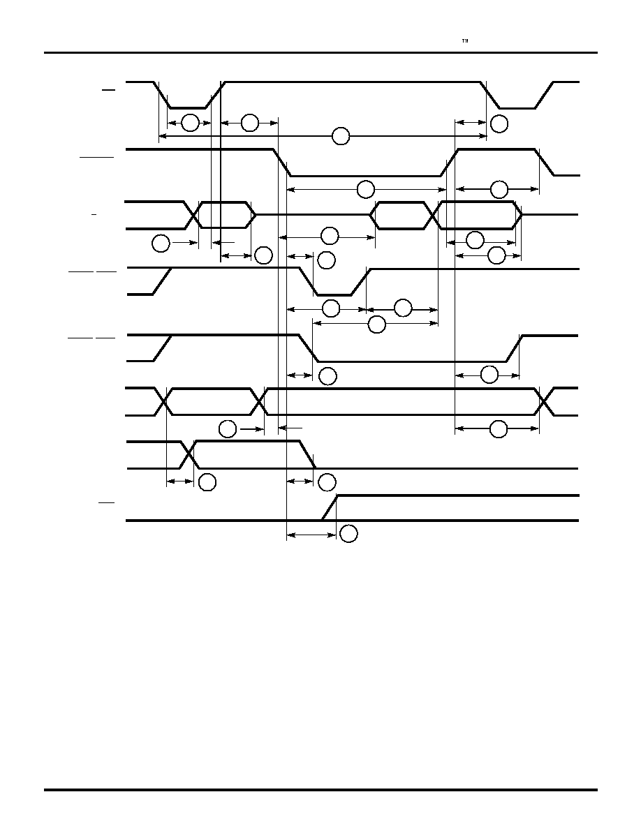
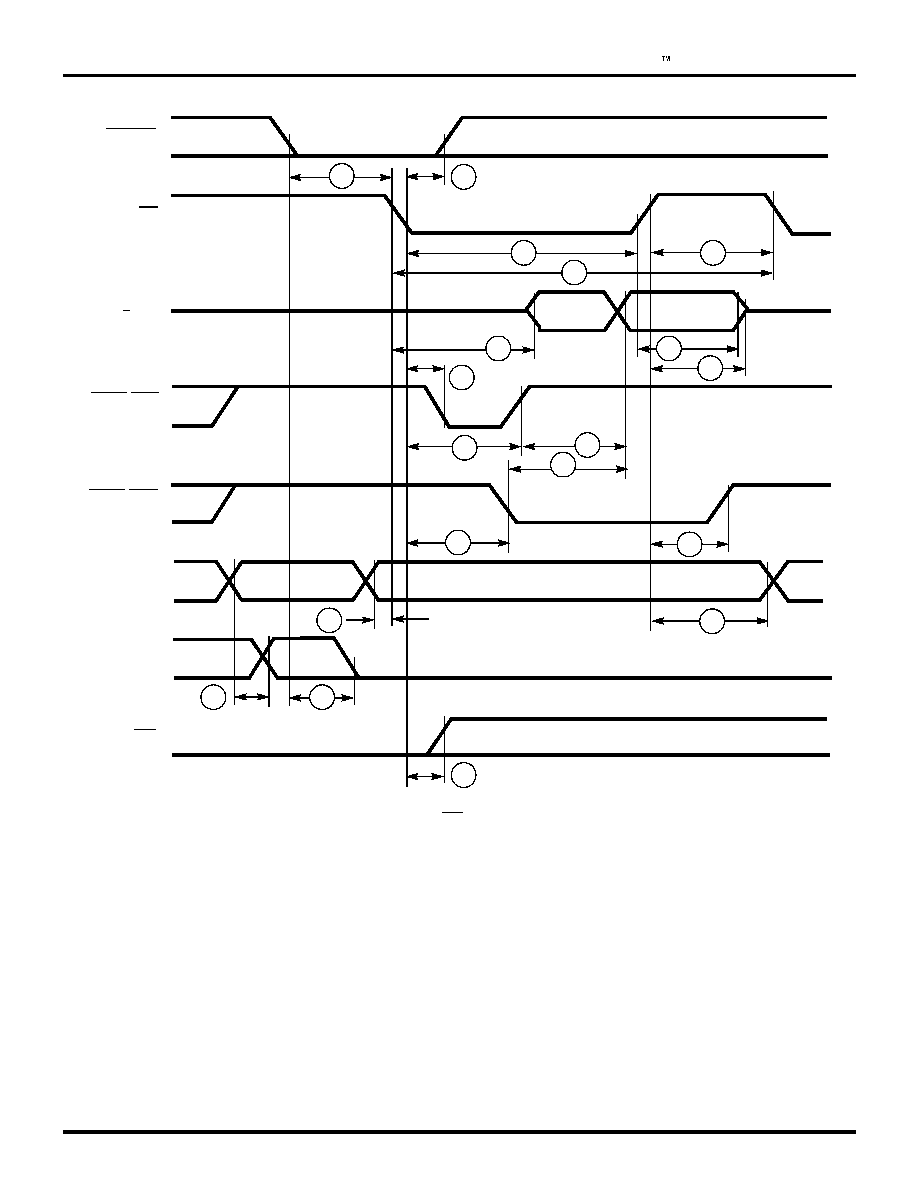
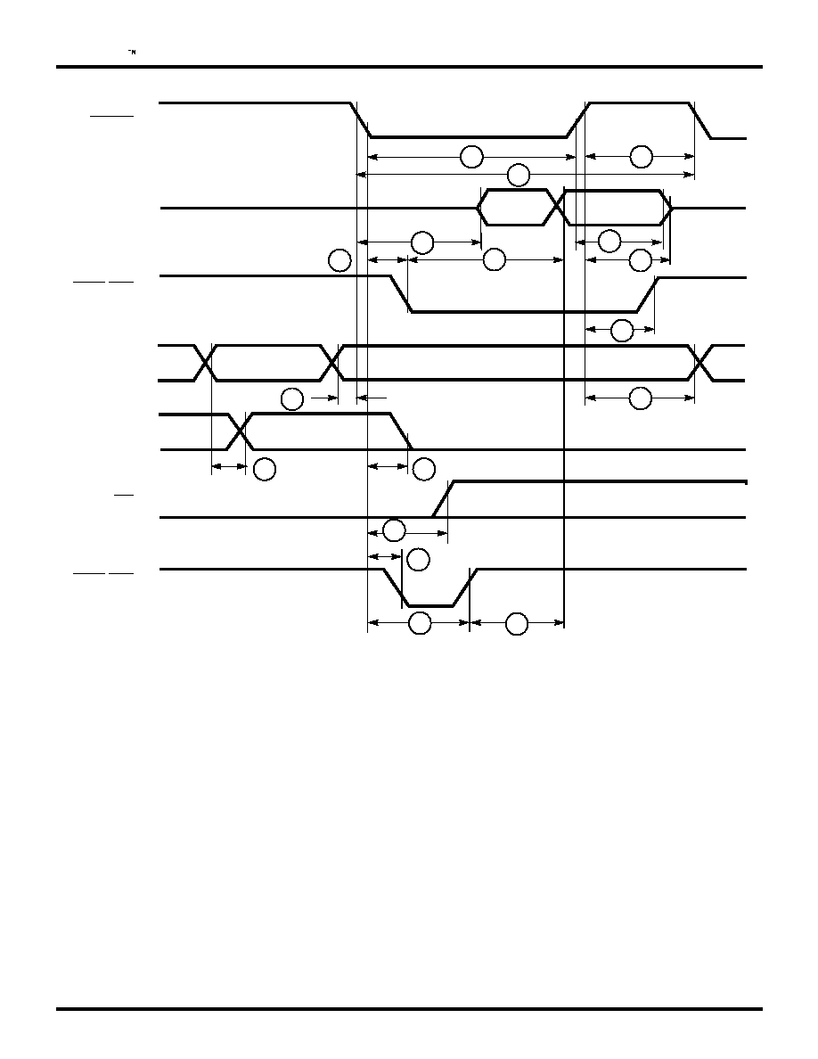
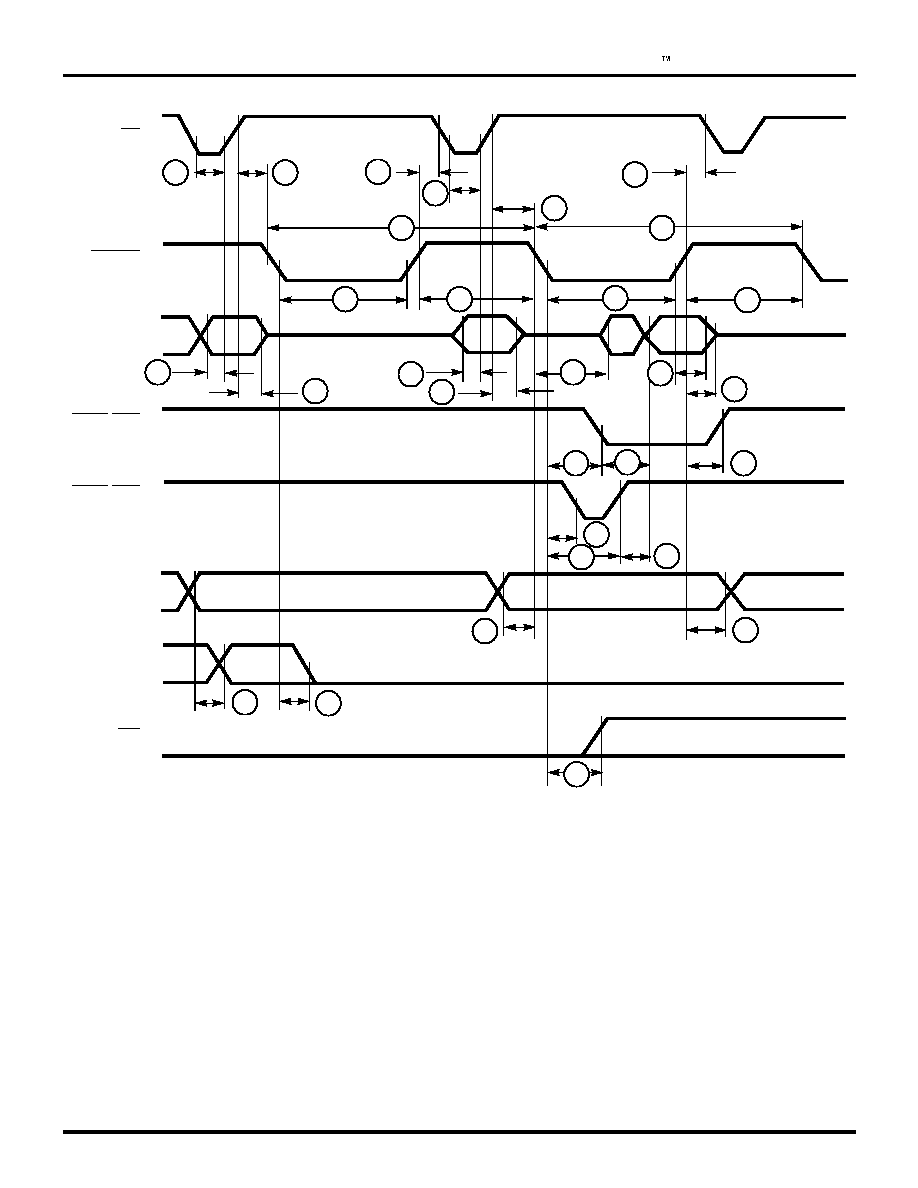
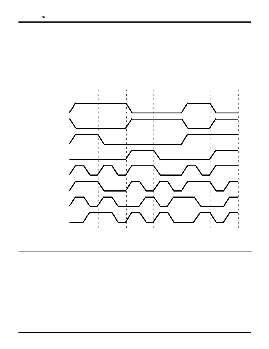
75% 6+/+0)
The USC interface timing is similar to that found on a static
RAM, except that it is much more flexible. Up to eight sep-
arate timing strobe signals may be present on the interface:
DS, RD, WR, PITACK, RxACKA, RxACKB, TxACKA
and TxACKB. Only one of these timing strobes may be ac-
tive at any time. Should the external logic activate more than
one of these strobes at the same time the USC will enter a
pre-reset state that is only exited by a hardware reset. Do
not allow overlap of timing strobes. The timing diagrams,
beginning on the next page, illustrate the different bus trans-
actions possible, with the necessary setup, hold and delay
times.
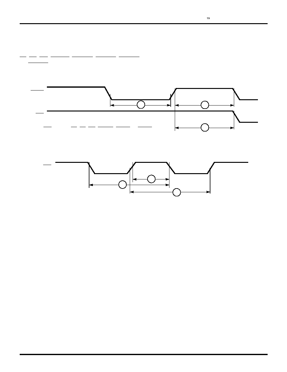
(KIWTG 4GUGV 6KOKPI
(KIWTG $WU %[ENG 6KOKPI
4'5'6
56$
0QVG 56$ KU CP[ QH &5 4& 94 2+6#%- 4Z#%- QT 6Z#%-
!
56$
<%
%/15 75% 7PKXGTUCN 5GTKCN %QPVTQNNGT
ZiLOG
&55%%
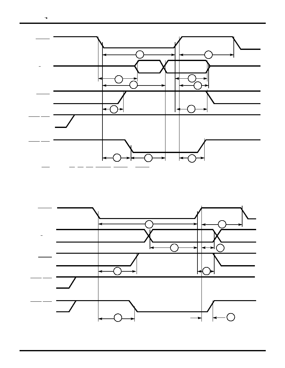
(KIWTG &/# 4GCF %[ENG
(KIWTG &/# 9TKVG %[ENG
4Z#%-
#& #&
4Z4'3
9#+64&;
9CKV
9#+64&;
4GCF[
0QVG 56$ KU CP[ QH &5 4& 94 2+6#%- 4Z#%- QT 6Z#%-
!
6Z#%-
#& #&
6Z4'3
9#+64&;
9CKV
9#+64&;
4GCF[

<%
ZiLOG
%/15 75% 7PKXGTUCN 5GTKCN %QPVTQNNGT
&55%%
(KIWTG /WNVKRNGZGF &5 4GCF %[ENG
%5
#$ &%
#%-
#5
49
&5
#& #&
4Z4'3
9#+64&;
9CKV
9#+64&;
4GCF[

<%
%/15 75% 7PKXGTUCN 5GTKCN %QPVTQNNGT
ZiLOG
&55%%
(KIWTG /WNVKRNGZGF &5 9TKVG %[ENG
%5
#$ &%
5+6#%-
#5
49
&5
#& #&
6Z4'3
9#+64&;
9CKV
9#+64&;
4GCF[
$

<%
ZiLOG
%/15 75% 7PKXGTUCN 5GTKCN %QPVTQNNGT
&55%%
(KIWTG /WNVKRNGZGF 4& 4GCF %[ENG
#$ &%
5+6#%-
#5
4&
#& #&
4Z4'3
9#+64&;
9CKV
9#+64&;
4GCF[
'
%5

<%
%/15 75% 7PKXGTUCN 5GTKCN %QPVTQNNGT
ZiLOG
&55%%
(KIWTG /WNVKRNGZGF 94 9TKVG %[ENG
$
%5
#$ &%
5+6#%-
#5
49
&5
#& #&
6Z4'3
9#+64&;
9CKV
9#+64&;
4GCF[
<%
ZiLOG
%/15 75% 7PKXGTUCN 5GTKCN %QPVTQNNGT
&55%%
(KIWTG 0QPOWNVKRNGZGF &5 4GCF %[ENG
#$ &%
5+6#%-
#5
94
#& #&
6Z4'3
9#+64&;
9CKV
9#+64&;
4GCF[
%5
%
&
<%
%/15 75% 7PKXGTUCN 5GTKCN %QPVTQNNGT
ZiLOG
&55%%
(KIWTG 0QPOWNVKRNGZGF &5 9TKVG %[ENG
#$ &%
5+6#%-
49
&5
#& #&
6Z4'3
9#+64&;
9CKV
9#+64&;
4GCF[
%5
$
<%
ZiLOG
%/15 75% 7PKXGTUCN 5GTKCN %QPVTQNNGT
&55%%
(KIWTG 0QPOWNVKRNGZGF 4& 4GCF %[ENG
#$ &%
5+6#%-
4&
#& #&
4Z4'3
9#+64&;
4GCF[
%5
9#+64&;
9CKV
'
<%
%/15 75% 7PKXGTUCN 5GTKCN %QPVTQNNGT
ZiLOG
&55%%
(KIWTG 0QPOWNVKRNGZGF 94 9TKVG %[ENG
#$ &%
5+6#%-
94
#& #&
6Z4'3
9#+64&;
4GCF[
%5
9#+64&;
9CKV
%
&
<%
ZiLOG
%/15 75% 7PKXGTUCN 5GTKCN %QPVTQNNGT
&55%%
(KIWTG /WNVKRNGZGF &5 +PVGTTWRV #EMPQYNGFIGF %[ENG
5+6#%-
&5
#& #&
9#+64&;
4GCF[
#5
9#+64&;
9CKV
+'+
+'1
+06

<%
%/15 75% 7PKXGTUCN 5GTKCN %QPVTQNNGT
ZiLOG
&55%%
(KIWTG /WNVKRNGZGF 4& +PVGTTWRV #EMPQYNGFIG %[ENG
5+6#%-
4&
#& #&
9#+64&;
4GCF[
#5
9#+64&;
9CKV
+'+
+'1
+06
<%
ZiLOG
%/15 75% 7PKXGTUCN 5GTKCN %QPVTQNNGT
&55%%
(KIWTG /WNVKRNGZGF 2WNUGF +PVGTTWRV #EMPQYNGFIG %[ENG
#5
2+6#%-
#& #&
9#+64&;
9CKV
9#+64&;
4GCF[
+'+
+'1
+06
'
%
&
!
"
#
$
<%
%/15 75% 7PKXGTUCN 5GTKCN %QPVTQNNGT
ZiLOG
&55%%
(KIWTG 0QPOWNVKRNGZGF &5 +PVGTTWRV #EMPQYNGFIG %[ENG
&5
5+6#%-
#& #&
9#+64&;
9CKV
9#+64&;
4GCF[
+'+
+'1
+06
<%
ZiLOG
%/15 75% 7PKXGTUCN 5GTKCN %QPVTQNNGT
&55%%
(KIWTG 0QPOWNVKRNGZGF 4& +PVGTTWRV #EMPQYNGFIG %[ENG
4&
5+6#%-
#& #&
9#+64&;
9CKV
9#+64&;
4GCF[
+'+
+'1
+06
<%
%/15 75% 7PKXGTUCN 5GTKCN %QPVTQNNGT
ZiLOG
&55%%
(KIWTG 0QPOWNVKRNGZGF 2WNUGF +PVGTTWRV #EMPQYNGFIG %[ENG
#& #&
9#+64&;
9CKV
9#+64&;
4GCF[
+'+
+'1
+06
2+6#%-
%
&
!
"
$
#
'
<%
ZiLOG
%/15 75% 7PKXGTUCN 5GTKCN %QPVTQNNGT
&55%%
(KIWTG /WNVKRNGZGF &QWDNG2WNUG +PVCEM %[ENG
#& #&
9#+64&;
9CKV
9#+64&;
4GCF[
+'+
+'1
+06
2+6#%-
2WNUG
#5
%
&
'
"
!
#
$

<%
%/15 75% 7PKXGTUCN 5GTKCN %QPVTQNNGT
ZiLOG
&55%%
(KIWTG 0QPOWNVKRNGZGF &QWDNG2WNUG +PVCEM %[ENG
#& #&
9#+64&;
9CKV
9#+64&;
4GCF[
+'+
+'1
+06
2+6#%-
2WNUG
%
&
'
!
"
#
$

<%
ZiLOG
%/15 75% 7PKXGTUCN 5GTKCN %QPVTQNNGT
&55%%
#% %*#4#%6'4+56+%5
<% )GPGTCN 6KOKPI
0Q
5[ODQN
2CTCOGVGT
/KP
/CZ
7PKVU
0QVGU
6U4Z&
4Z%T
4Z& VQ 4Z% 4KUG 5GVWR 6KOG
Z /QFG
PU
6J4Z&
4Z%T
4Z& VQ 4Z% 4KUG *QNF 6KOG
Z /QFG
PU
6U4ZF
4Z%H
4Z& VQ 4Z% (CNN 5GVWR 6KOG
Z /QFG
PU
6J4Z&
4Z%H
4Z& VQ 4Z% (CNN *QNF 6KOG
Z /QFG
PU
6U5[
4Z%
&%& CU 5;0% VQ 4Z% 4KUG 5GVWR 6KOG
PU
6J5[
4Z%
&%& CU 5;0% VQ 4Z% 4KUG *QNF 6KOG
Z /QFG
PU
6F6Z%H
6Z&
6Z% (CNN VQ 6Z& &GNC[
PU
6F6Z%T
6Z&
6Z% 4KUG VQ 6Z& &GNC[
PU
6Y4Z%J
4Z% *KIJ 9KFVJ
PU
6E4Z%
4Z% %[ENG 6KOG
PU
6Y6Z%J
6Z% *KIJ 9KFVJ
PU
6Y6Z%N
6Z% .QY 9KFVJ
PU
6E6Z%
6Z% %[ENG 6KOG
PU
6Y'Z6
&%& QT %65 2WNUG 9KFVJ
PU
695;
&%& CU 5;0% +PRWV 2WNUG 9KFVJ
PU
6Y%.-J
%.- *KIJ 9KFVJ
PU
6Y%.-+
%.- *KIJ 9KFVJ
PU
6E%.-
%.- %[ENG 6KOG
PU
0QVGU
4Z% KU 4Z% QT 6Z% YJKEJGXGT KU UWRRN[KPI VJG TGEGKXG ENQEM
6Z% KU 6Z% QT 4Z% YJKEJGXGT KU UWRRN[KPI VJG VTCPUOKV ENQEM
2CTCOGVGT CRRNKGU QPN[ VQ (/ GPEQFKPIFGEQFKPI
%.- KU 4Z% QT 6Z% YJGP UWRRN[KPI &2.. $4) QT %64 ENQEM
+06

<%
%/15 75% 7PKXGTUCN 5GTKCN %QPVTQNNGT
ZiLOG
&55%%
(KIWTG <% 5[UVGO 6KOKPI
4Z% 6Z%
4GEGKXG
4Z'3
4GSWGUV
+06
4Z% CU
4GEGKXGT
1WVRWV
4Z% 6Z%
6TCPUOKV
6Z4'3
6Z% CU
6TCPUOKVVGT
1WVRWV
%65 &%&
6Z4'3
4Z4'3
0QVG %.- KU 4Z% QT 6Z% YJGP UWRRN[KPI &2.. $4) QT %64 ENQEM
<%
ZiLOG
%/15 75% 7PKXGTUCN 5GTKCN %QPVTQNNGT
&55%%
<% 5[UVGO 6KOKPI
0Q
5[ODQN
2CTCOGVGT
/KP
/CZ
7PKVU
0QVGU
6F4Z%
4'3
4Z% 4KUG VQ 4Z4'3 8CNKF &GNC[
PU
6F4Z%
4Z%
6Z% 4KUG VQ 4Z% CU 4GEGKXGT 1WVRWV 8CNKF &GNC[
PU
6F4Z%
+06
4Z% 4KUG VQ +06 8CNKF &GNC[
PU
6F6Z%
4'3
6Z% (CNN VQ 6Z4'3 8CNKF &GNC[
PU
6F6Z%
6Z%
4Z% (CNN VQ 6Z% CU 6TCPUOKVVGT 1WVRWV 8CNKF &GNC[
PU
6F6Z%
+06
6Z% (CNN VQ +06 8CNKF &GNC[
PU
6F':6
+06
%65 &%& 6Z4'3 4Z4'3 VTCPUKVKQP VQ +06 8CNKF
&GNC[
PU
0QVGU
4Z% KU 4Z% QT 6Z% YJKEJGXGT KU UWRRN[KPI VJG TGEGKXG ENQEM
6Z% KU 6Z% QT 4Z% YJKEJGXGT KU UWRRN[KPI VJG VTCPUOKV ENQEM
<%
%/15 75% 7PKXGTUCN 5GTKCN %QPVTQNNGT
ZiLOG
&55%%
#4%*+6'%674'
The USC internal structure includes two completely inde-
pendent full-duplex serial channels, each with two baud rate
generators, a digital phase-locked loop for clock recovery,
transmit and receive character counters and a full-duplex
DMA interface. The two serial channels share a common
bus interface. The bus interface is designed to provide easy
interface to most microprocessors, whether they employ a
multiplexed or nonmultiplexed, 8-bit or16-bit bus structure.
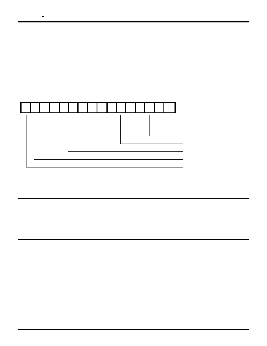
Each channel is controlled by a set of thirty 16-bit registers,
nearly all of which are readable and writable. There is one
additional 16-bit register in the bus interface used to con-
figure the nature of the bus interface. The BCR functions
are shown in below.
(KIWTG $WU %QPHKIWTCVKQP 4GIKUVGT
# 2#6*
Both the transmitter and the receiver in the channel are ac-
tually microcoded serial processors. As the data shifts
through the transmit or receive shift register, the microcode
watches for specific bit patterns, counts bits, and at the ap-
propriate time transfers data to or from the FIFOs. The mi-
crocode also checks status and generates status interrupts
as appropriate.
(70%6+10#. &'5%4+26+10
The functional capabilities of the USC are described from
two different points of view: as a data communications de-
vice, it transmits and receives data in a wide variety of data
communications protocols; as a microprocessor peripheral,
the USC offers such features as read/write registers, a flex-
ible bus interface, DMA interface support and vectored in-
terrupts.
&CVC %QOOWPKECVKQPU %CRCDKNKVKGU
The USC provides two independent full-duplex channels
programmable for use in any common data communication
protocol. The receiver and transmitter modes are complete-
ly independent, as are the two channels. Each receiver and
transmitter is supported by a 32-byte deep FIFO and a 16-
bit message length counter. All modes allow optional even,
odd, mark or space parity. Synchronous modes allow the
choice of two 16-bit or one 32-bit CRC polynomial. Selec-
tion of from one to eight bits-per-character is available in
both receiver and transmitter, independently. Error and sta-
tus conditions are carried with the data in the receive and
transmit FIFOs to greatly reduce the CPU overhead re-
quired to send or receive a message. Specific, appropriately
timed interrupts are available to signal such conditions as
overrun, parity error, framing error, end-of-frame, idle line
received, sync acquired, transmit underrun, CRC sent, clos-
&
&
&
&
&
&
&
&
&
&
&
&
&
&
&
&
#FFTGUU 0QPG
5JKHV 4KIJV #FFTGUUGU
&QWDNG2WNUG +06#%-
$KV $WU
�
4GUGTXGF
5VCVG #NN 2KPU
5GRCTCVG #FFTGUU HQT $KV $WU
� /WUV DG RTQITCOOGF CU

<%
ZiLOG
%/15 75% 7PKXGTUCN 5GTKCN %QPVTQNNGT
&55%%
ing sync/flag sent, abort sent, idle line sent and preamble
sent. In addition, several useful internal signals such as re-
ceive FIFO load, received sync, transmit FIFO read and
transmission complete may be sent to pins for use by ex-
ternal circuitry.
#U[PEJTQPQWU /QFG
The receiver and transmitter can
handle data at a rate of 1/16, 1/32, or 1/64 the clock rate.
The receiver rejects start bits less than one-half a bit time
and will not erroneously assemble characters following a
framing error. The transmitter is capable of sending one,
two, or anywhere in the range of 1/16 to two stop bits per
character in 1/16 bit increments.
'ZVGTPCN 5[PE /QFG
The receiver is synchronized to the
receive data stream by an externally-supplied signal on a
pin for custom protocol applications.
+UQEJTQPQWU /QFG
Both transmitter and receiver may op-
erate on start-stop (async) data using a 1x clock. The trans-
mitter can send one or two stop bits.
#U[PEJTQPQWU 9KVJ %QFG 8KQNCVKQPU
This is similar to
Isochronous mode except that the start bit is replaced by a
three bit-time code violation pattern as in MIL-STD 1553B.
The transmitter can send zero, one or two stop bits.
/QPQU[PE /QFG
In this mode, a single character is used
for synchronization. The sync character can be either eight
bits long with an arbitrary data character length, or pro-
grammed to match the data character length. The receiver
is capable of automatically stripping sync characters from
the received data stream. The transmitter may be pro-
grammed to automatically send CRC on either an underrun
or at the end of a programmed message length.
$KU[PE /QFG
This mode is identical to monosync mode
except that character synchronization requires two succes-
sive characters for synchronization. The two characters
need not be identical.
*&.% /QFG
In this mode, the receiver recognizes flags,
performs optional address matching, accommodates ex-
tended address fields, 8- or 16-bit control fields and logical
control fields, performs zero deletion and CRC checking.
The receiver is capable of receiving shared-zero flags, rec-
ognizes the abort sequence and can receive arbitrary length
messages. The transmitter automatically sends opening and
closing flags, performs zero insertion and can be pro-
grammed to send an abort, an extended abort, a flag or CRC
and a flag on transmit underrun. The transmitter can also
automatically send the closing flag with optional CRC at
the end of a programmed message length. Shared-zero flags
are selected in the transmitter and a separate character
length may be programmed for the last character in the
frame.
$KU[PE 6TCPURCTGPV /QFG
In this mode, the synchroniza-
tion pattern is DLE≠SYN, programmable selected from ei-
ther ASCII or EBCDIC encoding. The receiver recognizes
control character sequences and automatically handles
CRC calculation without CPU intervention. The transmitter
can be programmed to send either SYN, DLE≠SYN,
CRC≠SYN, or CRC≠DLE≠SYN upon underrun and can au-
tomatically send the closing DLE≠SYN with optional CRC
at the end of a programmed message length.
0$+2 /QFG
This mode is identical to async except that the
receiver checks for the status of an additional address/data
bit between the parity bit and the stop bit. The value of this
bit is FIFO'ed along with the data. This bit is automatically
inserted in the transmitter with the value that is FIFO'ed
with the transmit data.
/QFG
This mode implements the data format of
IEEE 802.3 with 16-bit address compare. In this mode,
DCD and CTS are used to implement the carrier sense and
collision detect interactions with the receiver and transmit-
ter.
5NCXGF /QPQU[PE /QFG
This mode is available only in
the transmitter and allows the transmitter (operating as
though it were in monosync mode) to send data that is byte-
synchronous to the data being received by the receiver.
*&.% .QQR /QFG
This mode is also available only in the
transmitter and allows the USC to be used in an HDLC loop
configuration. In this mode, the receiver is programmed to
operate in HDLC mode so that the transmitter echoes re-
ceived messages. Upon receipt of a particular bit pattern (ac-
tually a sequence of seven consecutive ones) the transmitter
breaks the loop and inserts its own frame(s).
&CVC 'PEQFKPI
The USC may be programmed to encode and decode the se-
rial data in any of eight different ways as shown in Figure
28. The transmitter encoding method is selected indepen-
dently of the receiver decoding method.
04<
In NRZ, a 1 is represented by a High level for the du-
ration of the bit cell and a 0 is represented by a Low level
for the duration of the bit cell.
04<$
Data is inverted from NRZ.
04<+/CTM
In NRZI-Mark, a 1 is represented by a transi-
tion at the beginning of the bit cell. That is, the level present
in the preceding bit cell is reversed. A 0 is represented by
the absence of a transition at the beginning of the bit cell.
04<+5RCEG
In NRZI-Space, a 1 is represented by the ab-
sence of a transition at the beginning of the bit cell. That is,
the level present in the preceding bit cell is maintained. A
<%
%/15 75% 7PKXGTUCN 5GTKCN %QPVTQNNGT
ZiLOG
&55%%
0 is represented by a transition at the beginning of the bit
cell.
$KRJCUG/CTM
In Biphase-Mark, a 1 is represented by a
transition at the beginning of the bit cell and another tran-
sition at the center of the bit cell. A 0 is represented by a
transition at the beginning of the bit cell only.
$KRJCUG5RCEG
In Biphase-Space, a 1 is represented by a
transition at the beginning of the bit cell only. A 0 is repre-
sented by a transition at the beginning of the bit cell and an-
other transition at the center of the bit cell.
$KRJCUG.GXGN
In Biphase-Level, a 1 is represented by a
High during the first half of the bit cell and a Low during
the second half of the bit cell. A 0 is represented by a Low
during the first half of the bit cell and a High during the sec-
ond half of the bit cell.
&KHHGTGPVKCN $KRJCUG.GXGN
In Differential Biphase-Level,
a "1" is represented by a transition at the center of the bit
cell, with the opposite polarity from the transition at the cen-
ter of the preceding bit cell. A 0 is represented by a transition
at the center of the bit cell with the same polarity as the tran-
sition at the center of the preceding bit cell. In both cases
there may be transitions at the beginning of the bit cell to
set up the level required to make the correct center transi-
tion.
%JCTCEVGT %QWPVGTU
Each channel in the USC contains a 16-bit character counter
for both receiver and transmitter. The receive character
counter may be preset either under software control or au-
tomatically at the beginning of a receive message. The
counter decrements with each receive character and at the
end of the receive message the current value in the counter
is automatically loaded into a four-deep FIFO. This allows
DMA transfer of data to proceed without CPU intervention
at the end of a received message, as the values in the FIFO
(KIWTG &CVC 'PEQFKPI
Data
1
1
0
0
1
0
NRZ
NRZB
NRZI-M
NRZI-S
BI-PHASE-M
BIPHASE-S
BIPHASE-L
DIFFERENTIAL
BIPHASE-L

<%
ZiLOG
%/15 75% 7PKXGTUCN 5GTKCN %QPVTQNNGT
&55%%
allow the CPU to determine message boundaries in mem-
ory. Similarly, the transmit character counter is loaded ei-
ther under software control or automatically at the begin-
ning of a transmit message. The counter is decremented with
each write to the transmit FIFO. When the counter has dec-
remented to 0, and that byte is sent, the transmitter auto-
matically terminates the message in the appropriate fashion
(usually CRC and the closing flag or sync character) without
requiring CPU intervention.
$CWF 4CVG )GPGTCVQTU
Each channel in the USC contains two baud rate generators.
Each generator consists of a 16-bit time constant register
and a 16-bit down counter. In operation, the counter decre-
ments with each baud rate generator clock, with the time
constant automatically reloaded when the count reaches ze-
ro. The output of the baud rate generator toggles when the
counter reaches a count of one-half of the time constant and
again when the counter reaches zero.A new time constant
may be written at any time but the new value will not take
effect until the next load of the counter. The outputs of both
baud rate generators are sent to the clock multiplexer for use
internally or externally. The baud rate generator output fre-
quency is related to the baud rate generator input clock fre-
quency by the following formula:
Output frequency = Input frequency/(time constant + 1).
This allows an output frequency in the range of 1 to 1/65536
of the input frequency, inclusive.
&KIKVCN 2JCUG.QEMGF .QQR
Each channel in the USC contains a Digital Phase-Locked
Loop (DPLL) to recover clock information from a data
stream with NRZI or Biphase encoding. The DPLL is driven
by a clock that is nominally 8, 16 or 32 times the receive
data rate. The DPLL uses this clock, along the data stream,
to construct a clock for the data. This clock may then be rout-
ed to the receiver, transmitter, or both, or to a pin for use
externally. In all modes, the DPLL counts the input clock
to create nominal bit times. As the clock is counted, the
DPLL watches the incoming data stream for transitions.
Whenever a transition is detected, the DPLL makes a count
adjustment (during the next counting cycle), to produce an
output clock which tracks the incoming bit cells. The DPLL
provides properly phased transmit and receive clocks to the
clock multiplexer.
%QWPVGTU
Each channel contains two 5-bit counters, which are pro-
grammed to divide an input clock by 4, 8, 16 or 32. The in-
puts of these two counters are sent to the clock multiplexer.
The counters are used as prescalers for the baud rate gen-
erators, or to provide a stable transmit clock from a common
source when the DPLL is providing the receive clock.
%NQEM /WNVKRNGZGT
The clock multiplexer in each channel selects the clock
source for the various blocks in the channel and selects an
internal clock signal to potentially be sent to either the RxC
or TxC pin.
6GUV /QFGU
The USC can be programmed for local loopback or auto
echo operation. In local loopback, the output of the trans-
mitter is internally routed to the input of the receiver. This
allows testing of the USC data paths without any external
logic. Auto echo connects the RxD pin directly to the TxD
pin. This is useful for testing serial links external to the USC.

<%
%/15 75% 7PKXGTUCN 5GTKCN %QPVTQNNGT
ZiLOG
&55%%
+1 +06'4(#%' %#2#$+.+6+'5
The USC offers the choice of polling, interrupt (vectored
or nonvectored) and block transfer modes to transfer data,
status and control information to and from the CPU.
2QNNKPI
All interrupts are disabled. The registers in the USC are au-
tomatically updated to reflect current status. The CPU polls
the Daisy Chain Control Register (DCCR) to determine sta-
tus changes and then reads the appropriate status register
to find and respond to the change in status. USC status bits
are grouped according to function to simplify this software
action.
+PVGTTWRV
When a USC responds to an interrupt acknowledge from
the CPU, an interrupt vector may be placed on the data bus.
This vector is held in the Interrupt Vector Register (IVR).
To speed interrupt response time, the USC modifies three
bits in this vector to indicate which type of interrupt is being
requested.
Each of the six sources of interrupts in each channel of the
USC (Receive Status, Receive Data, Transmit Status,
Transmit Data, I/O Status and Device Status) has three bits
associated with the interrupt source: Interrupt Pending (IP),
Interrupt-Under-Service (IUS) and Interrupt Enable (IE). If
the IE bit for a given source is set, that source can request
interrupts. Note that individual sources within the six
groups also have interrupt enable bits which are set for the
particular source. In addition, there is a Master Interrupt En-
able (MIE) bit in each channel which globally enables or
disables interrupts within the channel.
The other two bits are related to the interrupt priority chain.
A channel in the USC may request an interrupt only when
no higher priority interrupt source is requesting one, e.g.,
when IEI is High for the channel. In this case the channel
activates the INT signal. The CPU then responds with an
interrupt acknowledge cycle, and the interrupting channel
places a vector on the data bus.
In the USC, the IP bit signals that an interrupt request is be-
ing serviced. If an IUS is set, all interrupt sources of lower
priority within the channel and external to the channel are
prevented from requesting interrupts. The internal interrupt
sources are inhibited by the state of the internal daisy chain,
while lower priority devices are inhibited by the IEO output
of the channel being pulled Low and propagated to subse-
quent peripherals. An IUS bit is set during an interrupt ac-
knowledge cycle if there are no higher priority devices re-
questing interrupts.
There are six sources of interrupt in each channel: Receive
Status, Receive Data, Transmit Status, Transmit Data, I/O
Status and Device Status, prioritized in that order within the
channel. There are six sources of Receive Status interrupt,
each individually enabled: exited hunt, idle line,
break/abort, code violation/end-of-transmission/end-of-
frame, parity error and overrun error. The Receive Data in-
terrupt is generated whenever the receive FIFO fills with
data beyond the level programmed in the Receive Interrupt
Control Register (RICR).
There are six sources of Transmit Status interrupt, each in-
dividually enabled: preamble sent, idle line sent, abort sent,
end-of-frame/end-of-transmission sent, CRC sent and un-
derrun error. The Transmit Data interrupt is generated
whenever the transmit FIFO empties below the level pro-
grammed in the Transmit Interrupt Control Register
(TICR). The I/O Status interrupt serves to report transitions
on any of six pins. Interrupts are generated on either or both
edges with separate selection and enables for each pin. The
pins programmed to generate I/O Status interrupts are RxC,
TxC, RxREQ, TxREQ, DCD and CTS. These interrupts are
independent of the programmed function of the pins. The
Device Status interrupt has four separately enabled sources:
receive character count FIFO overflow, DPLL sync ac-
quired, BRG1 zero count and BRGO zero count.
$NQEM 6TCPUHGT /QFG
The USC accommodates block transfers through DMA
through the RxREQ, TxREQ, RxACK and TxACK pins.
The RxREQ signal is activated when the fill level of the re-
ceive FIFO exceeds the value programmed in the RICR. The
DMA may respond with either a normal bus transaction or
by activating the RxACK pin to read the data directly (fly-
by transfer). The TxREQ signal is activated when the empty
level of the transmit FIFO falls below the value pro-
grammed in the TICR. The DMA may respond either with
a normal bus transaction or by activating the TxACK pin
to write the data directly (fly-by transfer). The RxACK and
TxACK pin functions for this mode are controlled by the
Hardware Configuration Register (HCR). Then using the
RxACK and TxACK pins to transfer data, no chip select is
necessary; these are dedicated strobes for the appropriate
FIFO.

<%
ZiLOG
%/15 75% 7PKXGTUCN 5GTKCN %QPVTQNNGT
&55%%
241)4#//+0)
The registers in each USC channel are programmed by the
system to configure the channels. Before this can occur,
however, the system must program the bus interface by writ-
ing to the Bus Configuration Register (BCR). The BCR has
no specific address and is only accessible immediately after
a hardware reset of the device. The first write to the USC,
after a hardware reset, programs the BCR. From that time
on, the normal channel registers may be accessed. No spe-
cific address need be presented to the USC for the BCR write
because the first write after a hardware reset is automatically
programmed for the BCR.
In the multiplexed bus case, all registers are directly ad-
dressable through the address latched by AS at the begin-
ning of a bus transaction. The address is decoded from either
AD6≠AD0 or AD7≠AD1. This is controlled by the Shift
Right/Shift Left bit in the BCR. The address maps for these
two cases are shown in Table 2. The D/C pin is still used
to directly access the receive and transmit data registers
(RDR and TDR) in the multiplexed bus; if D/C is High the
address latched by AS is ignored and an access of RDR or
TDR is performed.
In the nonmultiplexed bus case, the registers in each channel
are accessed indirectly using the address pointer in the
Channel Command/Address Register (CCAR) in each
channel. The address of the desired register is first written
to the CCAR and then the selected register is accessed; the
pointer in the CCAR is automatically cleared after this ac-
cess. The RDR and TDR are accessed directly using the D/C
pin, without disturbing the contents of the pointer in the
CCAR.
There are two important things to note about the USC. First,
the Channel Reset bit in the CCAR places the channel in
the reset state. To exit this reset state either a word of all
zeros must be written to the CCAR (16-bit bus) or a byte
of all zeros must be written to the lower byte of the CCAR
(8-bit bus). The second thing to note is that after reset, the
transmit and receive clocks are not connected. The first
thing that should be done in any initialization sequence is
a write to the Clock Mode Control Register (CMCR) to se-
lect a clock source for the receiver and transmitter.
The register addressing is shown in Table 3 while the bit
assignments for the registers are shown in Figure 29.
6CDNG /WNVKRNGZGF $WU #FFTGUU #UUKIPOGPVU
#FFTGUU 5KIPCN
5JKHV .GHV
5JKHV 4KIJV
$[VG9QTF #EEGUU
#&
#&
#FFTGUU
#&
#&
#FFTGUU
#&
#&
#FFTGUU
#&
#&
#FFTGUU
#&
#&
#FFTGUU
#&
#&
7RRGT.QYGT $[VG 5GNGEV
#&
#&
<%
%/15 75% 7PKXGTUCN 5GTKCN %QPVTQNNGT
ZiLOG
&55%%
(KIWTG $%4 4GUGV 5GSWGPEG CPF $KV #UUKIPOGPVU
Rqq
Gxuxqqp
6
5¬Fqg¬Iq¬5S
H¬5S
5¬Tggiu
U¬T¬gp¬Cixpus
67R¬Wuq
67R
Wuq
Tggiu
&6u¬Wut
Sqggq
5ppq
&6u¬Wut
Sqggq
5ppq
$6u
67Ra c1
67Ra#c1
67Ra c1
67Ra#c1
67Ra c1
Hq(
Ttq¬qqiq¬r¬q¬ggiu¬ut¬g¬5S¬giuq¬hqqq¬qq¬¬
gp¬uixpus¬tq¬67R¬uq¬itq¬g¬yxuxqqp¬q¬r¬h
HGxuxqqp
6
&6u¬Wut
Sqggq
5ppq
&6u¬Wut
Sqggq
5ppq
$6u
67Ra c1
67Ra#c1
67Ra c1
67Ra#c1
67Ra c1

<%
ZiLOG
%/15 75% 7PKXGTUCN 5GTKCN %QPVTQNNGT
&55%%
6CDNG 4GIKUVGT #FFTGUU .KUV
#FFTGUU # #
%%#4
%JCPPGN %QOOCPF#FFTGUU
4GIKUVGT
%/4
%JCPPGN /QFG 4GIKUVGT
%%54
%JCPPGN %QOOCPF5VCVWU
4GIKUVGT
%%4
%JCPPGN %QPVTQN 4GIKUVGT
6/&4
6GUV /QFG &CVC 4GIKUVGT
6/%4
6GUV /QFG %QPVTQN 4GIKUVGT
%/%4 %NQEM /QFG %QPVTQN 4GIKUVGT
*%4
*CTFYCTG %QPHKIWTCVKQP 4GIKUVGT
+84
+PVGTTWRV 8GEVQT 4GIKUVGT
+1%4
+1 %QPVTQN 4GIKUVGT
+%4
+PVGTTWRV %QPVTQN 4GIKUVGT
&%%4
&CKU[%JCKP %QPVTQN 4GIKUVGT
/+54
/KUE +PVGTTWRV 5VCVWU 4GIKUVGT
5+%4
5VCVWU +PVGTTWRV %QPVTQN 4GIKUVGT
:
4&4
4GEGKXG &CVC 4GIKUVGT
4GCF 1PN[
4/4
4GEGKXG /QFG 4GIKUVGT
4%54
4GEGKXG %QOOCPF5VCVWU 4GIKUVGT
4+%4
4GEGKXG +PVGTTWRV %QPVTQN 4GIKUVGT
454
4GEGKXG 5[PE 4GIKUVGT
4%.4
4GEGKXG %QWPV .KOKV 4GIKUVGT
4%%4
4GEGKXG %JCTCEVGT %QWPV 4GIKUVGT
6%4
6KOG %QPUVCPV 4GIKUVGT
:
6&4
6TCPUOKV &CVC 4GIKUVGT
9TKVG
1PN[
6/4
6TCPUOKV /QFG 4GIKUVGT
6%54
6TCPUOKV %QOOCPF5VCVWU
4GIKUVGT
6+%4
6TCPUOKV +PVGTTWRV %QPVTQN
4GIKUVGT
654
6TCPUOKV 5[PE 4GIKUVGT
6%.4
6TCPUOKV %QWPV .KOKV 4GIKUVGT
6%%4
6TCPUOKV %JCTCEVGT %QWPV 4GIKUVGT
6%4
6KOG %QPUVCPV 4GIKUVGT
:::::
$%4
$WU %QPHKIWTCVKQP 4GIKUVGT
6CDNG 4GIKUVGT #FFTGUU .KUV
#FFTGUU # #
<%
%/15 75% 7PKXGTUCN 5GTKCN %QPVTQNNGT
ZiLOG
&55%%
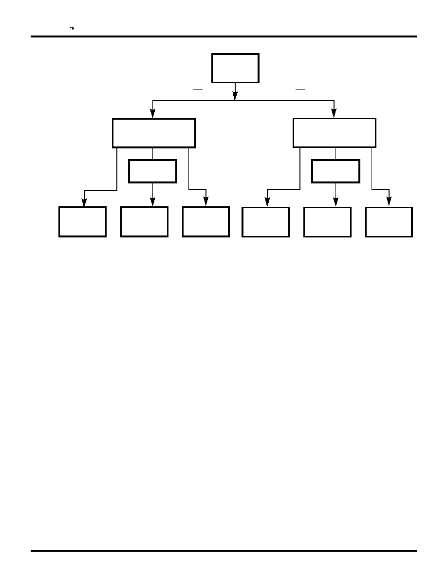
%10641. 4')+56'45
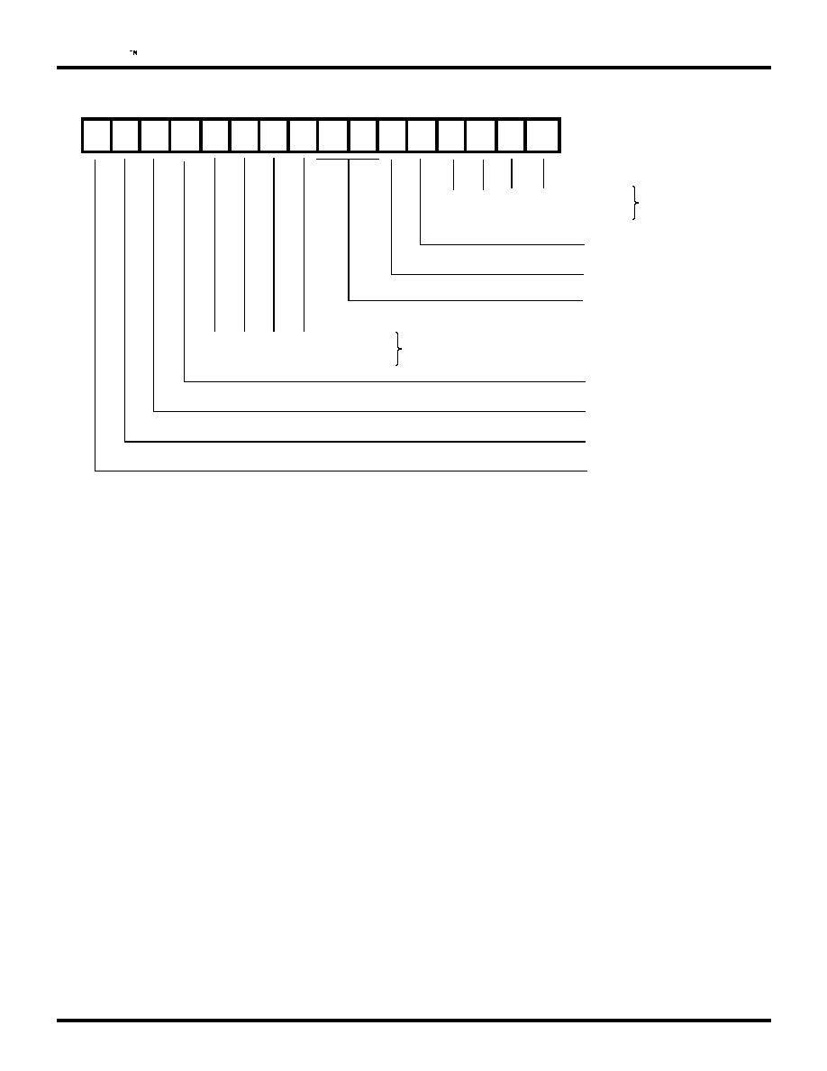
(KIWTG %JCPPGN %QOOCPF#FFTGUU 4GIKUVGT
7RRGT.QYGT $[VG 5GNGEV
9
#FFTGUU
9
#FFTGUU
9
#FFTGUU
9
#FFTGUU
9
#FFTGUU
9
$[VG9QTF #EEGUU
9
&/# %QPVKPWG
9
%JCPPGN 4GUGV
�5GNGEVGF CV 4GUGV
%JCPPGN
%QOOCPF
9
0QTOCN 1RGTCVKQP
#WVQ 'EJQ
'ZVGTPCN .QECN .QQRDCEM
+PVGTPCN .QECN .QQRDCEM
/QFG
%QPVTQN
&
&
&
&
&
&
&
&
&
&
&
&
&
&
&
&
#FFTGUU
0WNN %QOOCPF
4GUGTXGF
4GUGV *KIJGUV +75
4GUGTXGF
6TKIIGT %JCPPGN .QCF &/#
6TKIIGT 4Z &/#
6TKIIGT 6Z &/#
6TKIIGT 4Z
6Z &/#
4GUGTXGF
4Z (+(1 2WTIG
6Z (+(1 2WTIG
4Z
6Z (+(1 2WTIG
4GUGTXGF
.QCF 4Z %JCTCEVGT %QWPV
.QCF 6Z %JCTCEVGT %QWPV
.QCF 4Z
6Z %JCTCEVGT %QWPV
4GUGTXGF
.QCF 6%
.QCF 6%
.QCF 6%
6%
5GNGEV 5GTKCN &CVC .5$ (KTUV�
5GNGEV 5GTKCN &CVC /5$ (KTUV�
5GNGEV 5VTCKIJV /GOQT[ &CVC
5GNGEV 5YCRRGF /GOQT[ &CVC
4GUGTXGF
4Z 2WTIG
4GUGTXGF
4GUGTXGF
4GUGTXGF
4GUGTXGF
4GUGTXGF
4GUGTXGF
<%
ZiLOG
%/15 75% 7PKXGTUCN 5GTKCN %QPVTQNNGT
&55%%
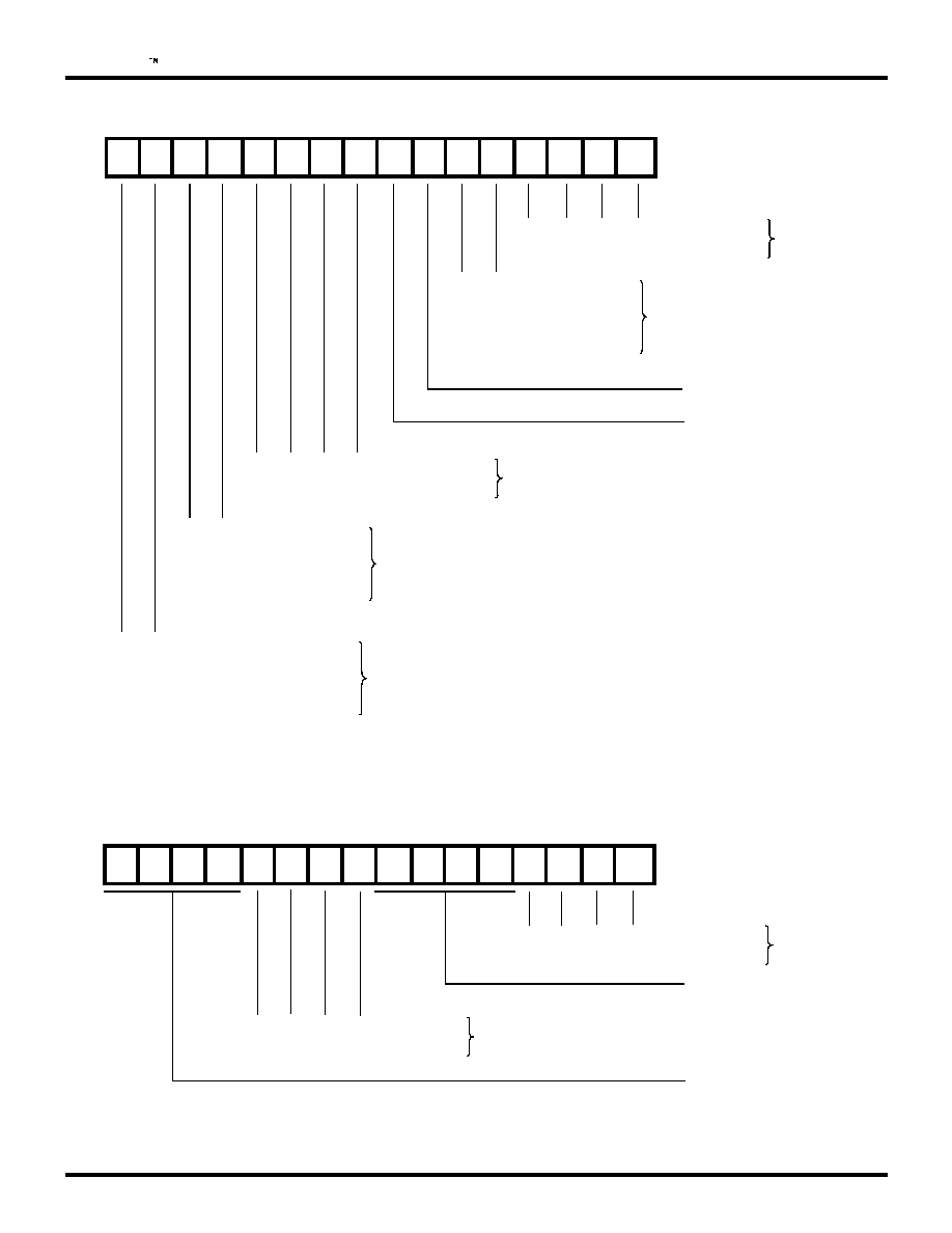
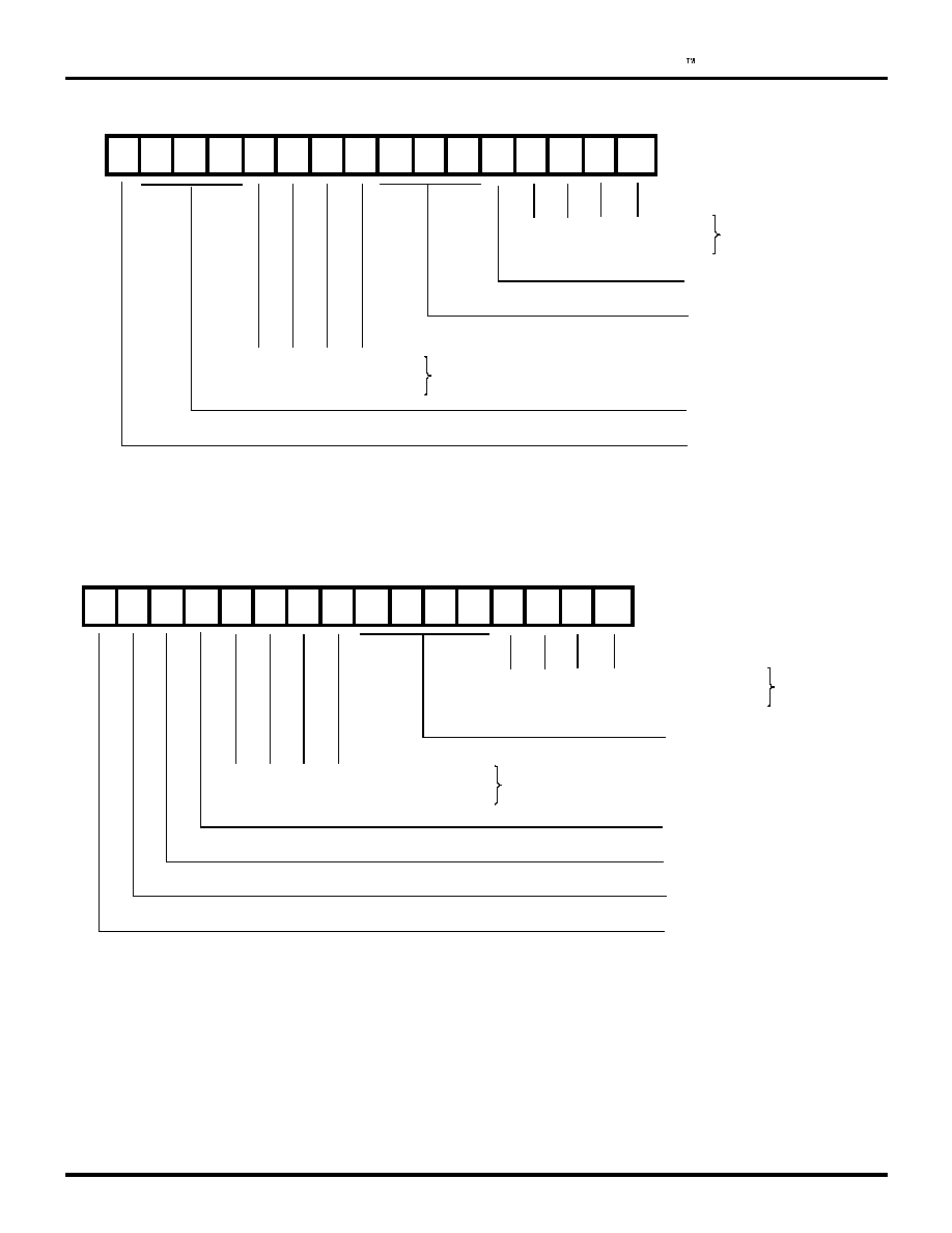
(KIWTG %JCPPGN /QFG 4GIKUVGT
#U[PEJTQPQWU
'ZVGTPCN U[PEJTQPQWU
+UQEJTQPQWU
#U[PEJTQPQWU YKVJ %8
/QPQU[PE
$KU[PE
*&.%
6TCPURCTGPV $KU[PE
0$+(
4GUGTXGF
4GUGTXGF
4GUGTXGF
4GUGTXGF
4GUGTXGF
4GUGTXGF
4GEGKXG
/QFG
4Z 5WDOQFG
4Z 5WDOQFG
4Z 5WDOQFG
4Z 5WDOQFG
#U[PEJTQPQWU
4GUGTXGF
+UQEJTQPQWU
#U[PEJTQPQWU YKVJ %8
/QPQU[PE
$KU[PE
*&.%
6TCPURCTGPV $KU[PE
0$+2
4GUGTXGF
4GUGTXGF
5NCXGF /QPQU[PE
4GUGTXGF
*&.% .QQR
4GUGTXGF
6TCPUOKVVGT
/QFG
6Z 5WDOQFG
6Z UWDOQFG
6Z 5WDOQFG
6Z UWDOQFG
&
&
&
&
&
&
&
&
&
&
&
&
&
&
&
&
#FFTGUU
<%
%/15 75% 7PKXGTUCN 5GTKCN %QPVTQNNGT
ZiLOG
&55%%
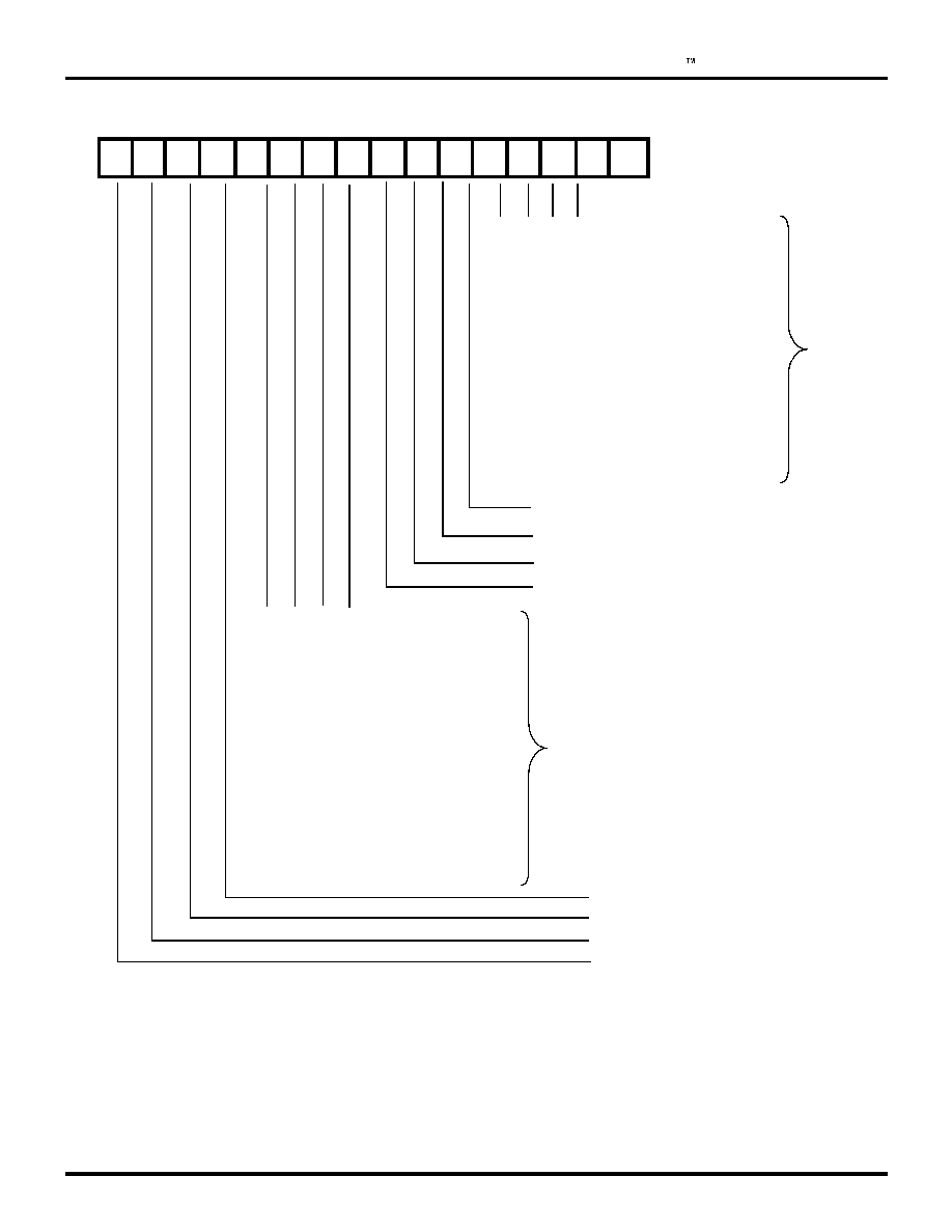
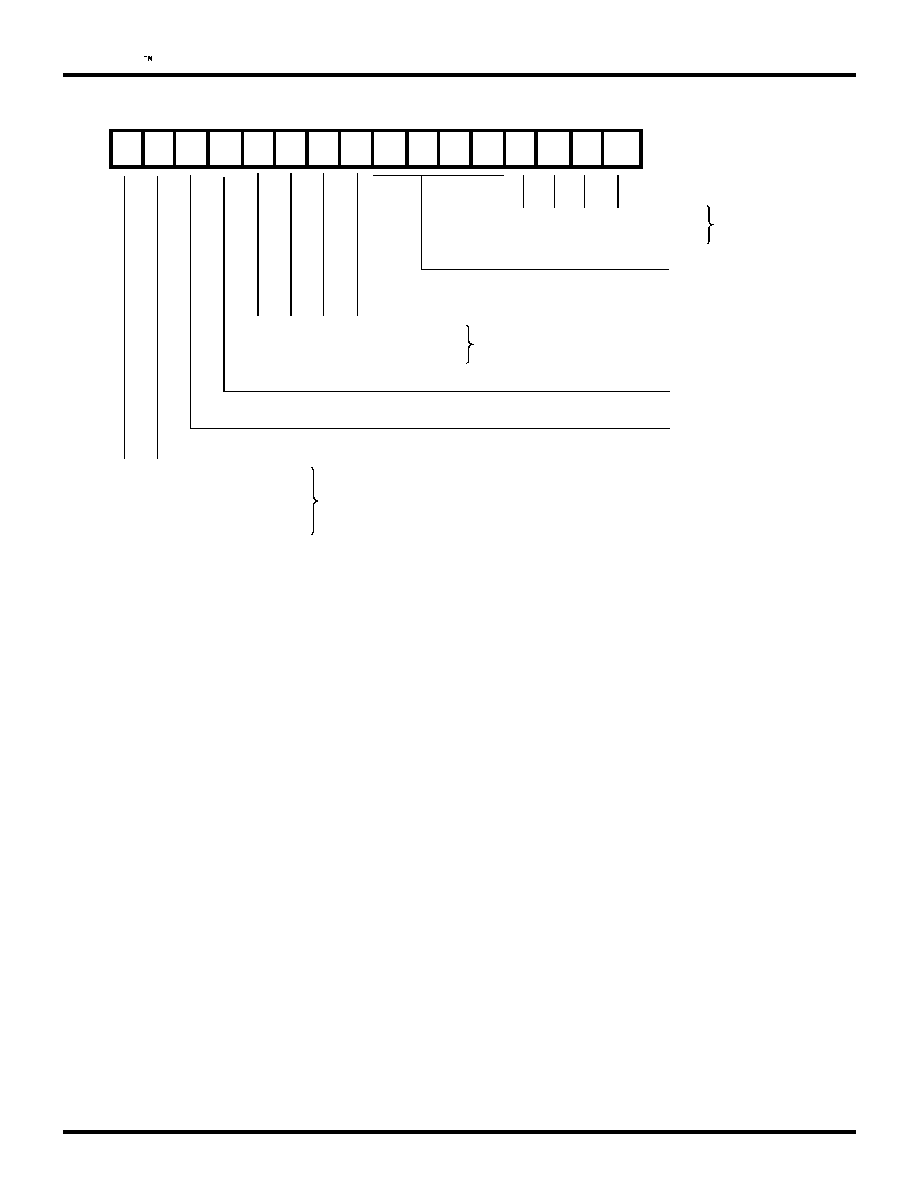
(KIWTG %JCPPGN /QFG 4GIKUVGT #U[PEJTQPQWU /QFG
(KIWTG %JCPPGN /QFG 4GIKUVGT 'ZVGTPCN 5[PE /QFG
&
&
&
&
&
&
&
&
&
&
&
&
&
&
&
&
#FFTGUU
#U[PEJTQPQWU
4GEGKXGT
/QFG
: &CVC 4CVG
: &CVC 4CVG
: &CVC 4CVG
4GUGTXGF
4Z %NQEM 4CVG
4GUGTXGF
4GUGTXGF
#U[PEJTQPQWU
6TCPUOKVVGT
/QFG
: &CVC 4CVG
: &CVC 4CVG
: &CVC 4CVG
4GUGTXGF
6Z %NQEM 4CVG
1PG 5VQR $KV
6YQ 5VQR $KVU
1PG 5QR $KV 5JCTGF
6YQ 5VQR $KVU 5JCTGF
6Z 5VQR $KVU
&
&
&
&
&
&
&
&
&
&
&
&
&
&
&
&
#FFTGUU
4GEGKXGT
/QFG
6TCPUOKVVGT
/QFG
'ZVGTPCN 5[PE
4GUGTXGF
4GUGTXGF
4GUGTXGF

<%
ZiLOG
%/15 75% 7PKXGTUCN 5GTKCN %QPVTQNNGT
&55%%
(KIWTG %JCPPGN /QFG 4GIKUVGT +UQEJTQPQWU /QFG
(KIWTG %JCPPGN /QFG 4GIKUVGT #U[PEJTQPQWU /QFG YKVJ
%QFG 8KQNCVKQP
/+. 56&
&
&
&
&
&
&
&
&
&
&
&
&
&
&
&
&
#FFTGUU
4GEGKXGT
+UQEJTQPQWU
/QFG
6TCPUOKVVGT
+UQEJTQPQWU
/QFG
4GUGTXGF
6Z 6YQ 5VQR $KVU
4GUGTXGF
4GUGTXGF
&
&
&
&
&
&
&
&
&
&
&
&
&
&
&
&
#FFTGUU
#U[PEJTQPQWU YKVJ %8
4GEGKXGT
/QFG
4Z 'ZVGPFGF 9QTF
4GUGTXGF
#U[PEJTQPQWU YKVJ %8
6TCPUOKVVGT
/QFG
%8 2QNCTKV[
6Z 'ZVGPFGF 9QTF
1PG 5VQR $KV
6YQ 5VQR $KVU
0Q 5VQR $KV
4GUGTXGF
6Z 5VQR $KVU
<%
%/15 75% 7PKXGTUCN 5GTKCN %QPVTQNNGT
ZiLOG
&55%%
(KIWTG %JCPPGN /QFG 4GIKUVGT /QPQU[PE /QFG
&
&
&
&
&
&
&
&
&
&
&
&
&
&
&
&
#FFTGUU
4GEGKXGT
/QFG
/QPQU[PE
/QPQU[PE
6TCPUOKVVGT
/QFG
4Z 5JQTV 5[PE %JCTCEVGT
4Z 5[PE 5VTKR
4GUGTXGF
6Z 5JQTV 5[PE %JCTCEVGT
6Z 2TGCODNG 'PCDNG
4GUGTXGF
6Z %4% QP 7PFGTTWP

<%
ZiLOG
%/15 75% 7PKXGTUCN 5GTKCN %QPVTQNNGT
&55%%
(KIWTG %JCPPGN /QFG 4GIKUVGT $KU[PE /QFG
&
&
&
&
&
&
&
&
&
&
&
&
&
&
&
&
#FFTGUU
4GEGKXGT
/QFG
$KU[PE
$KU[PE
6TCPUOKVVGT
/QFG
4Z 5JQTV 5[PE %JCTCEVGT
4Z 5[PE 5VTKR
4GUGTXGF
6Z 5JQTV 5[PE %JCTCEVGT
6Z 2TGCODNG 'PCDNG
5;0
5;05;0
%4%5;0
%4%5;05;0
6Z
7PFGTTWP
%QPFKVKQP

<%
%/15 75% 7PKXGTUCN 5GTKCN %QPVTQNNGT
ZiLOG
&55%%
(KIWTG %JCPPGN /QFG 4GIKUVGT *&.% /QFG
&
&
&
&
&
&
&
&
&
&
&
&
&
&
&
&
#FFTGUU
4GEGKXGT
/QFG
*&.%
*&.%
6TCPUOKVVGT
/QFG
5JCTGF <GTQ (NCIU
6Z 2TGCODNG 'PCDNG
#DQTV
'ZVGPFGF #DQTV
(NCI
%4%(NCI
6Z
7PFGTTWP
%QPFKVKQP
&KUCDNGF
1PG $[VG 0Q %QPVTQN
1PG $[VG 2NWU %QPVTQN
'ZVGPFGF 2NWU %QPVTQN
4Z #FFTGUU
5GCTEJ
/QFG
4Z $KV %QPVTQN
4Z .QIKECN
%QPVTQN 'PCDNG
<%
ZiLOG
%/15 75% 7PKXGTUCN 5GTKCN %QPVTQNNGT
&55%%
(KIWTG %JCPPGN /QFG 4GIKUVGT 6TCPURCTGPV $KU[PE /QFG
&
&
&
&
&
&
&
&
&
&
&
&
&
&
&
&
#FFTGUU
4GEGKXGT
/QFG
6TCPURCTGPV $KU[PE
6TCPURCTGPV $KU[PE
6TCPUOKVVGT
/QFG
'$%&+%
4GUGTXGF
'$%&+%
6Z 2TGCODNG 'PCDNG
5;0
&.'5;0
%4%5;0
%4%&.'5;0
6Z
7PFGTTWP
%QPFKVKQP
<%
%/15 75% 7PKXGTUCN 5GTKCN %QPVTQNNGT
ZiLOG
&55%%
(KIWTG %JCPPGN /QFG 4GIKUVGT 0$+2 /QFG
&
&
&
&
&
&
&
&
&
&
&
&
&
&
&
&
#FFTGUU
4GEGKXGT
/QFG
0$+2
0$+2
6TCPUOKVVGT
/QFG
: &CVC 4CVG
: &CVC 4CVG
: &CVC 4CVG
4GUGTXGF
4Z 2CTKV[ QP &CVC
4GUGTXGF
: &CVC 4CVG
: &CVC 4CVG
: &CVC 4CVG
4GUGTXGF
6Z 2CTKV[ QP &CVC
6Z #FFTGUU $KV
6Z %NQEM
4CVG
<%
ZiLOG
%/15 75% 7PKXGTUCN 5GTKCN %QPVTQNNGT
&55%%
(KIWTG %JCPPGN /QFG 4GIKUVGT /QFG
(KIWTG %JCPPGN /QFG 4GIKUVGT 5NCXGF /QPQU[PE /QFG
&
&
&
&
&
&
&
&
&
&
&
&
&
&
&
&
#FFTGUU
4GEGKXGT
/QFG
6TCPUOKVVGT
/QFG
4Z #FFTGUU 5GCTEJ
4GUGTXGF
6Z %4% QP 7PFGTTWP
4GUGTXGF
&
&
&
&
&
&
&
&
&
&
&
&
&
&
&
&
#FFTGUU
4GEGKXGT
/QFG
4GUGTXGF
5NCXGF /QPQU[PE
6TCPUOKVVGT
/QFG
4GUGTXGF
4GUGTXGF
6Z 5JQTV 5[PE %JCTCEVGT
6Z #EVKXG QP 4GEGKXGF 5[PE
6Z %4% QP 7PFGTTWP
<%
%/15 75% 7PKXGTUCN 5GTKCN %QPVTQNNGT
ZiLOG
&55%%
(KIWTG %JCPPGN /QFG 4GIKUVGT *&.% .QQR /QFG
&
&
&
&
&
&
&
&
&
&
&
&
&
&
&
&
#FFTGUU
4GEGKXGT
/QFG
4GUGTXGF
*&.% .QQR
5JCTGF <GTQ (NCIU
6Z #EVKXG QP 2QNN
#DQTV
'ZVGPFGF #DQTV
(NCI
%4%(NCI
6Z
7PFGTTWP
%QPFKVKQP
4GUGTXGF
6TCPUOKVVGT
/QFG

<%
ZiLOG
%/15 75% 7PKXGTUCN 5GTKCN %QPVTQNNGT
&55%%
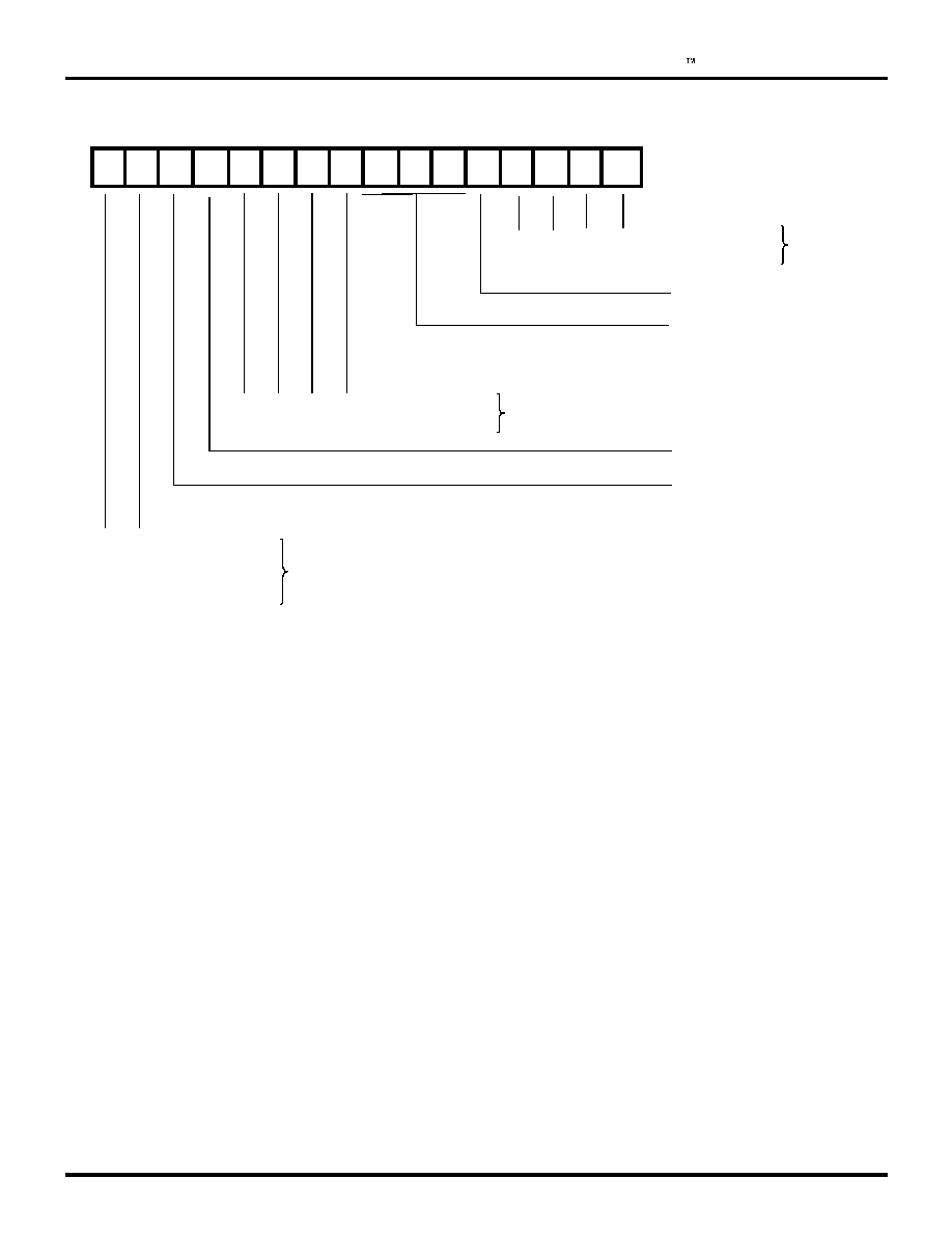
(KIWTG %JCPPGN %QOOCPF5VCVWU 4GIKUVGT
&
&
&
&
&
&
&
&
&
&
&
&
&
&
&
&
#FFTGUU
$KVU
$KV
$KVU
$KVU
$KVU
$KVU
$KVU
$KVU
$QVJ 'FIGU
4KUKPI 'FIG 1PN[
(CNNKPI 'FIG 1PN[
#FLWUV5[PE +PRWV
&2..
#FLWUV
5[PE 'FIG
*&.% 6Z .CUV
%JCTCEVGT .GPIVJ
4GUGTXGF
.QQR 5GPFKPI
4
1P .QQR
4
%NQEM /KUUGF .CVEJGF7PNCVEJ
%NQEMU /KUUGF .CVEJGF7PNCVEJ
&2.. KP 5[PE3WKEM 5[PE
4%% (+(1 %NGCT
9
4%% (+(1 8CNKF
4
4%% (+(1 1XGTHNQY
4
4Z#%-
4
6Z#%-
4

<%
%/15 75% 7PKXGTUCN 5GTKCN %QPVTQNNGT
ZiLOG
&55%%
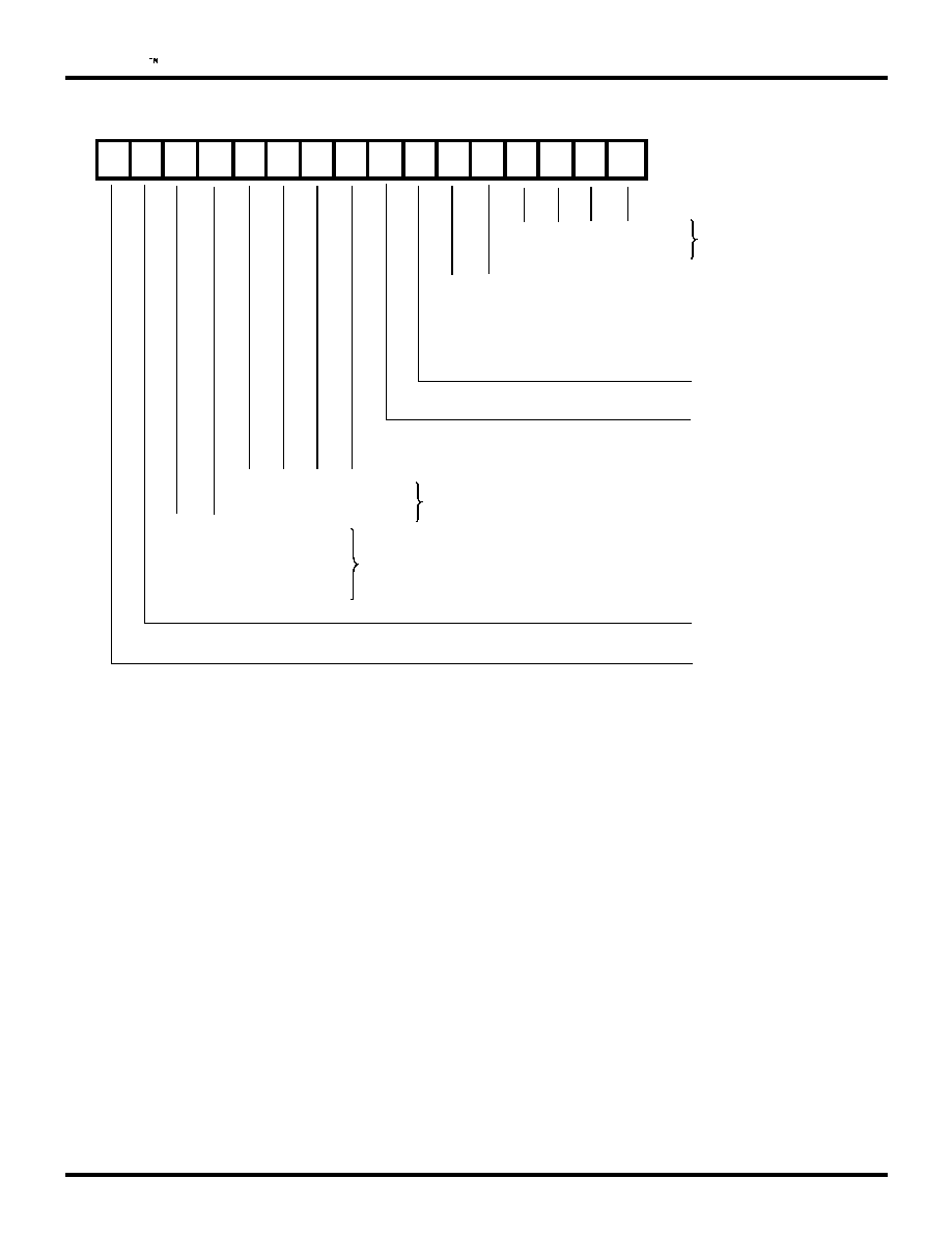
(KIWTG %JCPPGN %QPVTQN 4GIKUVGT
(KIWTG 2TKOCT[ 4GUGTXGF 4GIKUVGT
&
&
&
&
&
&
&
&
&
&
&
&
&
&
&
&
#FFTGUU
$KVU
$KVU
$KVU
$KVU
6Z 2TGCODNG
.GPIVJ
#NN <GTQU
#NN 1PGU
#NVGTPCVKPI CPF
#NVGTPCVKPI CPF
6Z 2TGCODNG
2CVVGTP
0Q 5VCVWU $NQEM
1PG 9QTF 5VCVWU $NQEM
6YQ 9QTF 5VCVWU $NQEM
4GUGTXGF
4Z 5VCVWU
$NQEM 6TCPUHGT
4GUGTXGF
9CKV HQT 4Z &/# 6TKIIGT
#NN 5[PE
6Z (NCI 2TGCODNG
9CKV HQT 6Z &/# 6TKIIGT
6Z 5JCXGF $KV .GPIVJ
#U[PE 1PN[
0Q 5VCVWU $NQEM
1PG 9QTF 5VCVWU $NQEM
6YQ 9QTF 5VCVWU $NQEM
4GUGTXGF
6Z 5VCVWU
$NQEM 6TCPUHGT
&
&
&
&
&
&
&
&
&
&
&
&
&
&
&
&
#FFTGUU
4GUGTXGF

<%
ZiLOG
%/15 75% 7PKXGTUCN 5GTKCN %QPVTQNNGT
&55%%
(KIWTG 5GEQPFCT[ 4GUGTXGF 4GIKUVGT
(KIWTG 6GUV /QFG &CVC 4GIKUVGT
&
&
&
&
&
&
&
&
&
&
&
&
&
&
&
&
#FFTGUU
4GUGTXGF
&
&
&
&
&
&
&
&
&
&
&
&
&
&
&
&
#FFTGUU
6GUV &CVC
6GUV &CVC
6GUV &CVC
6GUV &CVC
6GUV &CVC
6GUV &CVC
6GUV &CVC
6GUV &CVC
6GUV &CVC
6GUV &CVC
6GUV &CVC
6GUV &CVC
6GUV &CVC
6GUV &CVC
6GUV &CVC
6GUV &CVC

<%
%/15 75% 7PKXGTUCN 5GTKCN %QPVTQNNGT
ZiLOG
&55%%
(KIWTG 6GUV /QFG %QPVTQN 4GIKUVGT
&
&
&
&
&
&
&
&
&
&
&
&
&
&
&
&
#FFTGUU
0WNN #FFTGUU
*KIJ $[VG QH 5JKHVGTU
%4% $[VG
%4% $[VG
4Z (+(1
9TKVG
%NQEM /WNVKRNGZGT 1WVRWVU
%64 CPF %64 %QWPVGTU
%NQEM /WNVKRNGZGT +PRWVU
&2.. 5VCVWU
.QY $[VG QH 5JKHVGTU
%4% $[VG
%4% $[VG
6Z (+(1
4GCF
4GUGTXGF
+1 CPF &GXKEG 5VCVWU .CVEJGU
+PVGTPCN &CKU[ %JCKP
4GUGTXGF
4GUGTXGF
4GUGTXGF
4GUGTXGF
4GUGTXGF
4GUGTXGF
4GUGTXGF
4GUGTXGF
*
*
*
*
*
*
*
*
4GUGTXGF
6GUV
4GIKUVGT
#FFTGUU
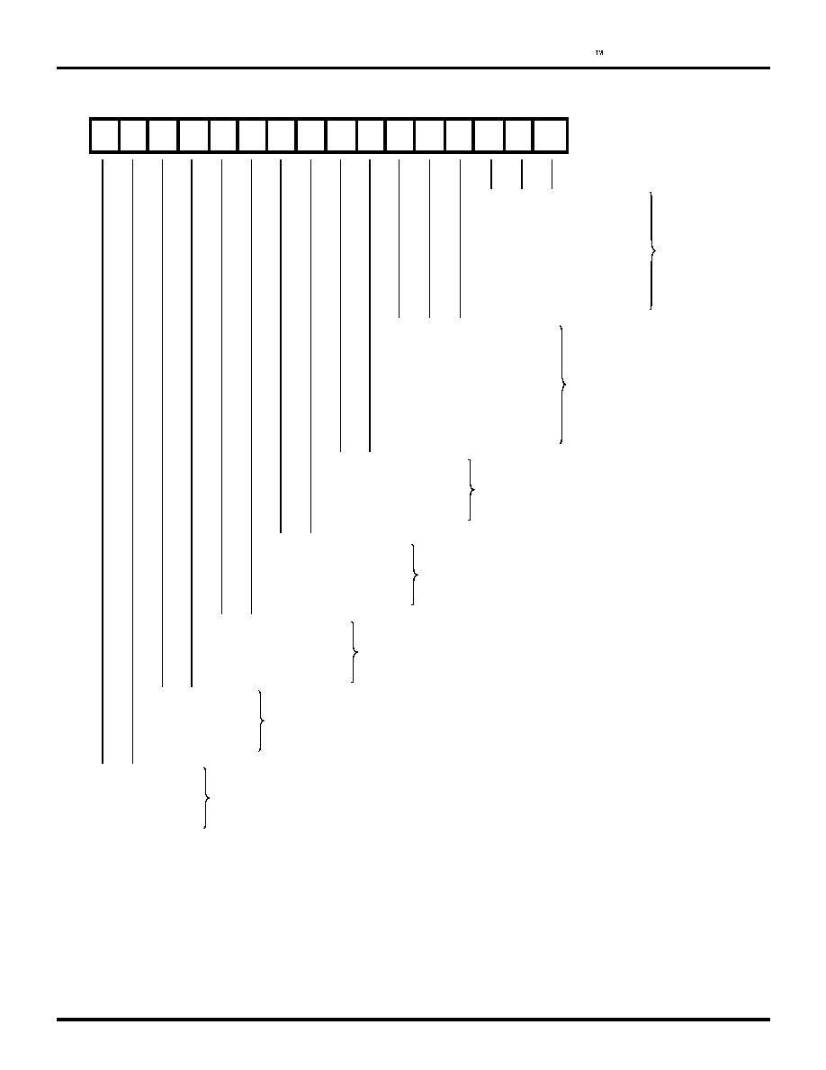
<%
ZiLOG
%/15 75% 7PKXGTUCN 5GTKCN %QPVTQNNGT
&55%%
(KIWTG %NQEM /QFG %QPVTQN 4GIKUVGT
&
&
&
&
&
&
&
&
&
&
&
&
&
&
&
&
#FFTGUU
&KUCDNGF
4Z% 2KP
6Z% 2KP
&2.. 1WVRWV
$4) 1WVRWV
$4) 1WVRWV
%64 1WVRWV
%64 1WVRWV
&KUCDNGF
4Z% 2KP
6Z% 2KP
&2.. 1WVRWV
$4) 1WVRWV
$4) 1WVRWV
%64 1WVRWV
%64 1WVRWV
%64 1WVRWV
%64 1WVRWV
4Z% 2KP
6Z% 2KP
$4) 1WVRWV
$4) 1WVRWV
4Z% 2KP
6Z% 2KP
%64 1WVRWV
%64 1WVRWV
4Z% 2KP
6Z% 2KP
&KUCDNGF
&KUCDNGF
4Z% 2KP
6Z% 2KP
&KUCDNGF
&KUCDNGF
4Z% 2KP
6Z% 2KP
%64 %NQEM
5QWTEG
%64 %NQEM
5QWTEG
$4) %NQEM
5QWTEG
$4) %NQEM
5QWTEG
&2.. %NQEM
5QWTEG
6TCPUOKV %NQEM
5QWTEG
4GEGKXG %NQEM
5QWTEG
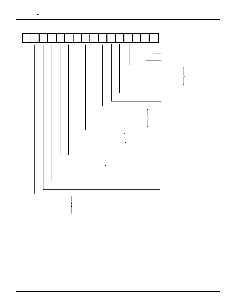
<%
%/15 75% 7PKXGTUCN 5GTKCN %QPVTQNNGT
ZiLOG
&55%%
(KIWTG *CTFYCTG %QPHKIWTCVKQP 4GIKUVGT
&
&
&
&
&
&
&
&
&
&
&
&
&
&
&
&
#FFTGUU
&KUCDNGF
04<04<+
$KRJCUG/CTM5RCEG
$KRJCUG.GXGN
Z %NQEM /QFG
Z %NQEM /QFG
Z %NQEM /QFG
Z %NQEM /QFG
6Z#%-
2KP %QPVTQN
%64 %NQEM
4CVG
&2.. %NQEM
4CVG
&2..
/QFG
$4) 'PCDNG
$4) 5KPING %[ENG%QPVKPWQWU
5VCVG 1WVRWV
4Z #EMPQYNGFIG +PRWV
1WVRWV
1WVRWV
$4) 'PCDNG
$4) UKPING %[ENGEQPVKPWQWU
5VCVG 1WVRWV
6Z #EMPQYNGFIG +PRWV
1WVRWV
1WVRWV
Z %NQEM /QFG
Z %NQEM /QFG
Z %NQEM /QFG
4GUGTXGF
4Z#%-
2KP %QPVTQN
#EEGRV %QFG 8KQNCVKQPU
%64 4CVG /CVEJ &2..%64
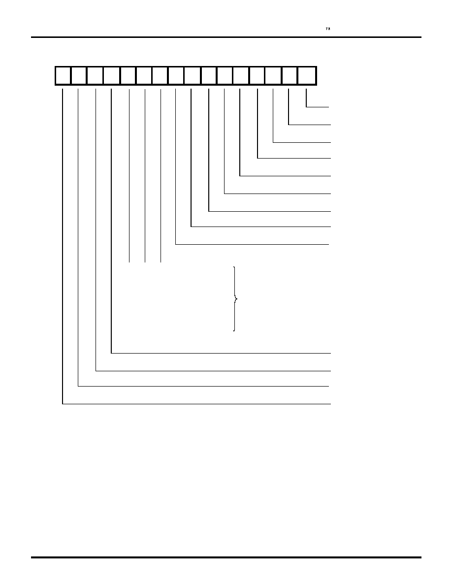
<%
ZiLOG
%/15 75% 7PKXGTUCN 5GTKCN %QPVTQNNGT
&55%%
(KIWTG +PVGTTWRV 8GEVQT 4GIKUVGT
&
&
&
&
&
&
&
&
&
&
&
&
&
&
&
&
#FFTGUU
+8
+8
+8
+8
+8
+8
+8
+8
+8
4
+8
4
+8
4
+8
4
+8
4
0QPG
&GXKEG 5VCVWU
+1 5VCVWU
6TCPUOKV &CVC
6TCPUOKV 5VCVWU
4GEGKXG &CVC
4GEGKXG 5VCVWU
0QV 7UGF
/QFKHKGF
8GEVQT
4

<%
%/15 75% 7PKXGTUCN 5GTKCN %QPVTQNNGT
ZiLOG
&55%%
(KIWTG +1 %QPVTQN 4GIKUVGT
&
&
&
&
&
&
&
&
&
&
&
&
&
&
&
&
#FFTGUU
+PRWV 2KP
4Z %NQEM 1WVRWV
4Z $[VG %NQEM 1WVRWV
5;0% 1WVRWV
$4) 1WVRWV
$4) 1WVRWV
%64 1WVRWV
&2.. 4Z 1WVRWV
+PRWV 2KP
6Z ENQEM 1WVRWV
6Z $[VG ENQEM 1WVRWV
6Z %QORNGVG 1WVRWV
$4) 1WVRWV
$4) 1WVRWV
%64 1WVRWV
&2.. 1WVRWV
5VCVG 1WVRWV
4Z 4GSWGUV 1WVRWV
1WVRWV
1WVRWV
6Z &CVC 1WVRWV
5VCVG 1WVRWV
1WVRWV
1WVRWV
5VCVG 1WVRWV
6Z 4GSWGUV 1WVRWV
1WVRWV
1WVRWV
&%& +PRWV
&%&5;0% +PRWV
1WVRWV
1WVRWV
%65 +PRWV
%65 +PRWV
1WVRWV
1WVRWV
%65 2KP
%QPVTQN
&%& 2KP
%QPVTQN
6Z4'3 2KP
%QPVTQN
4Z4'3 2KP
%QPVTQN
6Z& 2KP
%QPVTQN
6Z% 2KP
%QPVTQN
4Z% 2KP
%QPVTQN
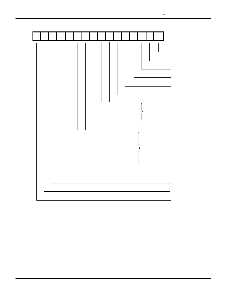
<%
ZiLOG
%/15 75% 7PKXGTUCN 5GTKCN %QPVTQNNGT
&55%%
(KIWTG +PVGTTWRV %QPVTQN 4GIKUVGT
&
&
&
&
&
&
&
&
&
&
&
&
&
&
&
&
#FFTGUU
&GXKEG 5VCVWU +'
+1 5VCVWU +'
6TCPUOKV &CVC +'
6TCPUOKV 5VCVWU +'
4GEGKXG &CVC +'
4GEGKXG 5VCVWU +'
4GEGKXGF
8+5
08
&.%
/+'
#NN
#NN
+1 5VCVWU CPF #DQXG
6TCPUOKV &CVC CPF #DQXG
6TCPUOKV 5VCVWU CPF #DQXG
4GEGKXG &CVC
4GEGKXG 5VCVWU 1PN[
0QPG
8+5
.GXGN
0WNN EQOOCPF
0WNN EQOOCPF
4GUGV +'
5GV +'
+' %QOOCPF
9
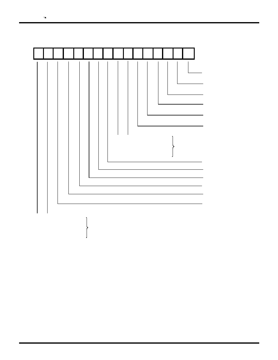
<%
%/15 75% 7PKXGTUCN 5GTKCN %QPVTQNNGT
ZiLOG
&55%%
(KIWTG &CKU[%JCKP %QPVTQN 4GIKUVGT
&
&
&
&
&
&
&
&
&
&
&
&
&
&
&
&
#FFTGUU
&GXKEG 5VCVWU +2
+1 5VCVWU +2
6TCPUOKV &CVC +2
6TCPUOKV 5VCVWU +2
4GEGKXG &CVC +2
4GEGKXG 5VCVWU +2
&GXKEG 5VCVWU +75
+1 5VCVWU +75
6TCPUOKV &CVC +75
6TCPUOKV 5VCVWU +75
4GEGKXG &CVC +75
0WNN EQOOCPF
4GUGV +2 CPF +75
4GUGV +2
5GV +2
+2 %QOOCPF
9
0WNN EQOOCPF
0WNN EQOOCPF
4GUGV +75
5GV +75
+75 %QOOCPF
9
4GEGKXG 5VCVWU +75
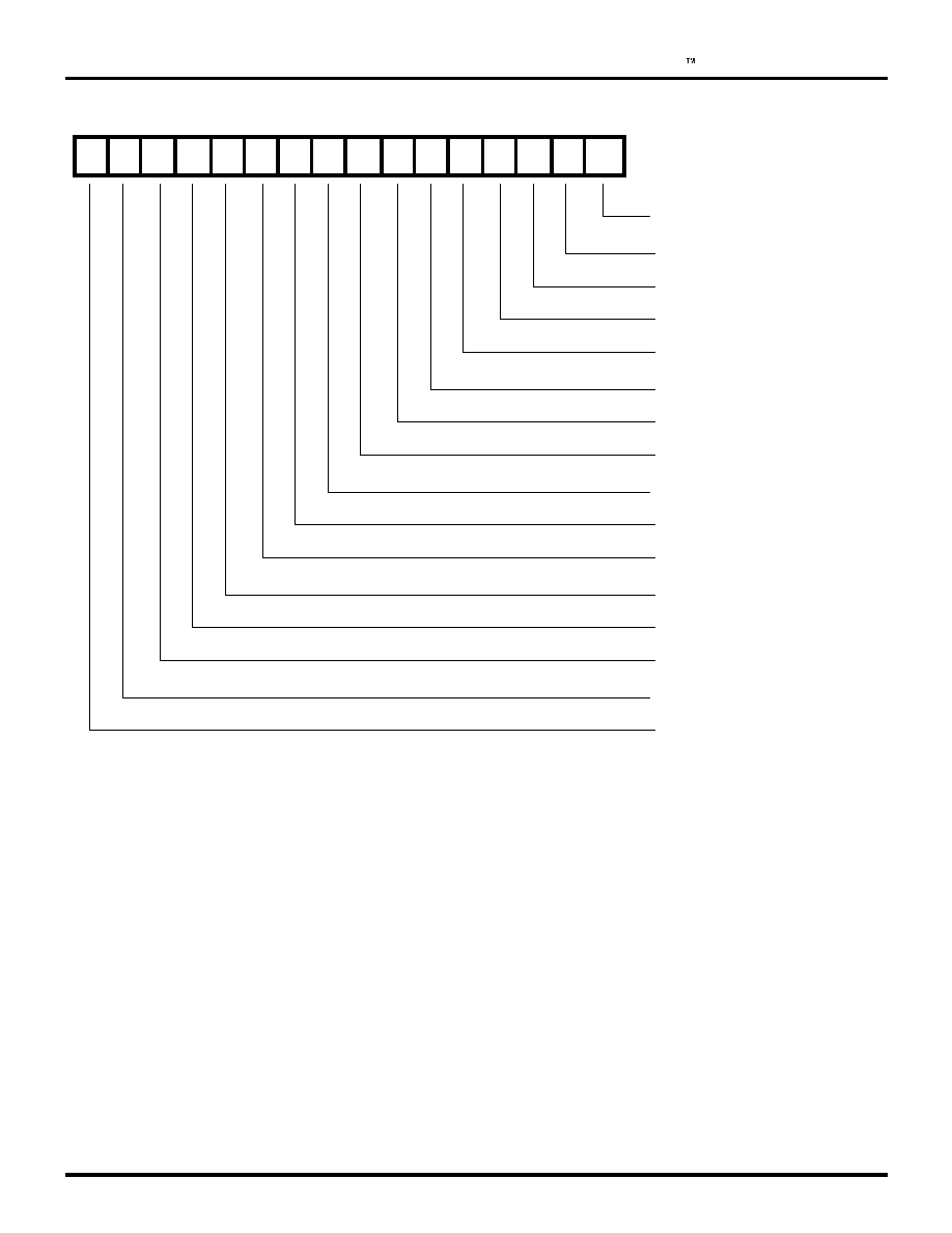
<%
ZiLOG
%/15 75% 7PKXGTUCN 5GTKCN %QPVTQNNGT
&55%%
(KIWTG /KUEGNNCPGQWU +PVGTTWRV 5VCVWU 4GIKUVGT
&
&
&
&
&
&
&
&
&
&
&
&
&
&
&
&
#FFTGUU
$4) <% .CVEJGF7PNCVEJ
$4) <% NCVEJGF7PNCVEJ
&2.. 5;0% NCVEJGF7PNCVEJ
4%% 1XGTHNQY .CVEJGF7PNCVEJ
%65
4
%65 .CVEJGF7PNCVEJ
&%&
4
&%& .CVEJGF7PNCVEJ
6Z4'3
4
6Z4'3 .CVEJGF7PNCVEJ
4Z4'3
4
4Z4'3 .CVEJGF7PNCVEJ
6Z%
4
6Z% .CVEJGF7PNCVEJ
4Z%
4
4Z% .CVEJGF7PNCVEJ
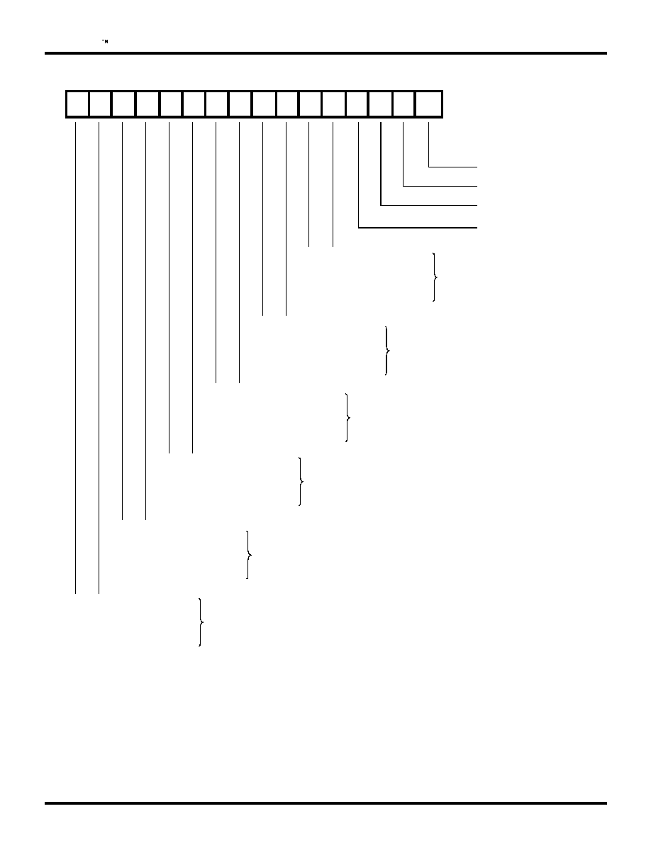
<%
%/15 75% 7PKXGTUCN 5GTKCN %QPVTQNNGT
ZiLOG
&55%%
(KIWTG 5VCVWU +PVGTTWRV %QPVTQN 4GIKUVGT
&KUCDNGF
4KUKPI 'FIG 1PN[
(CNNKPI 'FIG 1PN[
$QVJ 'FIGU
%65
+PVGTTWRVU
&%&
+PVGTTWRVU
&KUCDNGF
4KUKPI 'FIG 1PN[
(CNNKPI 'FIG 1PN[
$QVJ 'FIGU
6Z4'3
+PVGTTWRVU
&KUCDNGF
4KUKPI 'FIG 1PN[
(CNNKPI 'FIG 1PN[
$QVJ 'FIGU
&KUCDNGF
4KUKPI 'FIG 1PN[
(CNNKPI 'FIG 1PN[
$QVJ 'FIGU
4Z4'3
+PVGTTWRVU
6Z%
+PVGTTWRVU
&KUCDNGF
4KUKPI 'FIG 1PN[
(CNNKPI 'FIG 1PN[
$QVJ 'FIGU
4Z%
+PVGTTWRVU
$4) <% +'
$4) <% +'
&2.. 5;0% +'
4%% 1XGTHNQY +'
&KUCDNGF
4KUKPI 'FIG 1PN[
(CNNKPI 'FIG 1PN[
$QVJ 'FIGU
&
&
&
&
&
&
&
&
&
&
&
&
&
&
&
&
#FFTGUU
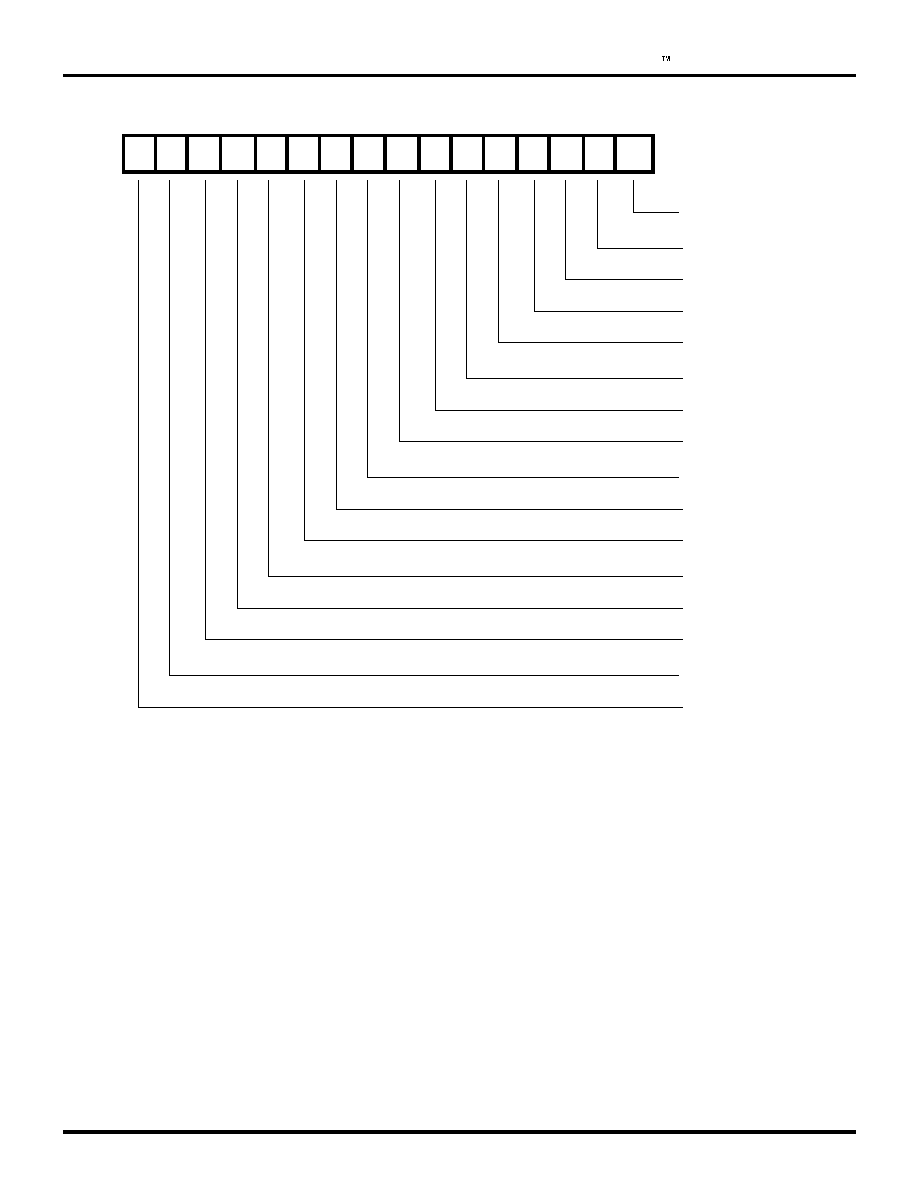
<%
ZiLOG
%/15 75% 7PKXGTUCN 5GTKCN %QPVTQNNGT
&55%%
(KIWTG 4GEGKXG &CVC 4GIKUVGT
&
&
&
&
&
&
&
&
&
&
&
&
&
&
&
&
#FFTGUU Z
4Z 
4
4Z 
4
4Z 
4
4Z 
4
4Z 
4
4Z 
4
4Z 
4
4Z 
4
4Z 
4
4Z 
4
4Z 
4
4Z 
4
4Z 
4
4Z 
4
4Z 
4
4Z 
4
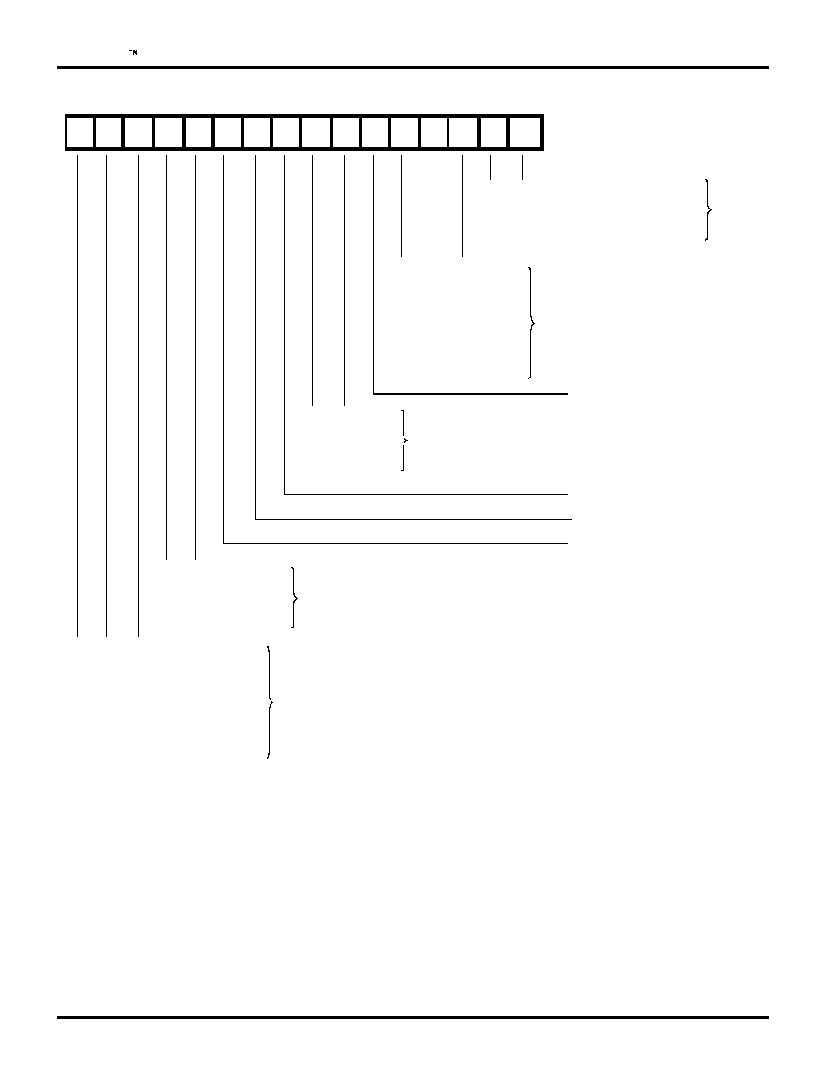
<%
%/15 75% 7PKXGTUCN 5GTKCN %QPVTQNNGT
ZiLOG
&55%%
(KIWTG 4GEGKXG /QFG 4GIKUVGT
&
&
&
&
&
&
&
&
&
&
&
&
&
&
&
&
#FFTGUU
&KUCDNG +OOGFKCVGN[
&KUCDNG #HVGT 4GEGRVKQP
'PCDNG 9KVJQWV #WVQ'PCDNGU
'PCDNG 9KVJ #WVQ'PCDNG
4Z
'PCDNG
$KVU
$KV
$KVU
$KVU
$KVU
$KVU
$KVU
$KVU
4Z %JCTCEVGT
.GPIVJ
'XGP
1FF
5RCEG
/CTM
4Z 2CTKV[
5GPUG
%4%%%+66
%4%
%4%
4GUGTXGF
4Z %4%
2QN[PQOKCN
04<
04<$
04<+/CTM
04<+5RCEG
$KRJCUG/CTM
$KRJCUG5RCEG
$KRJCUG.GXGN
&KHH $KRJCUG.GXGN
4Z &CVC
&GEQFKPI
3WGWG #DQTV
4Z %4% 'PCDNG
4Z %4% 2TGUGV 8CNWG
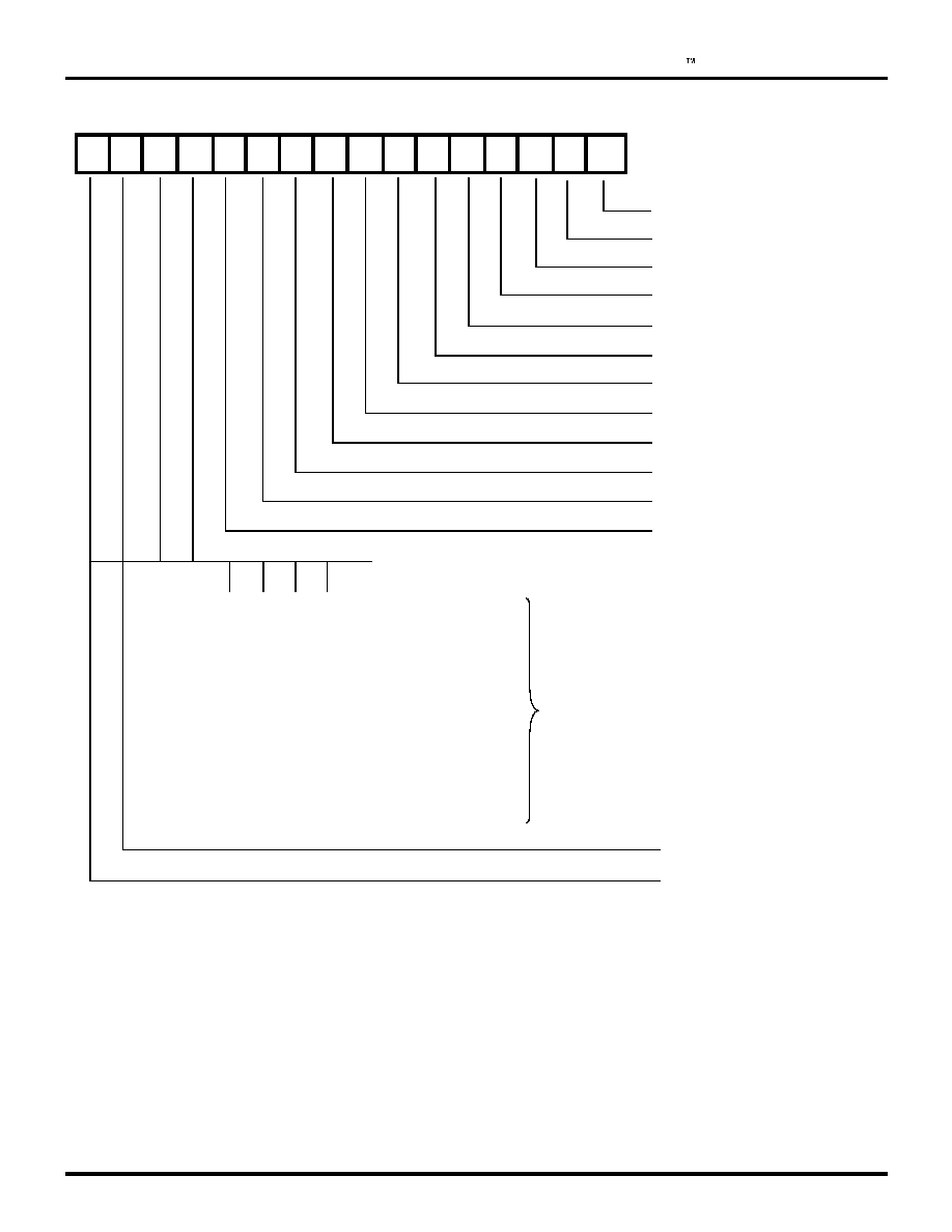
<%
ZiLOG
%/15 75% 7PKXGTUCN 5GTKCN %QPVTQNNGT
&55%%
(KIWTG 4GEGKXG %QOOCPF 5VCVWU 4GIKUVGT
0WNN %QOOCPF
4GUGTXGF
2TGUGV %4%
'PVGT *WPV /QFG
4GUGTXGF
5GNGEV (+(1 5VCVWU
5GNGEV (+(1 +PVGTTWRV .GXGN
5GNGEV (+(1 5VCVWU .GXGN
4GUGTXGF
4GUGTXGF
4GUGTXGF
4GUGTXGF
4GUGTXGF
4GUGTXGF
4GUGTXGF
4GUGTXGF
&
&
&
&
&
&
&
&
&
&
&
&
&
&
&
&
#FFTGUU
4GEGKXG
%QOOCPF
4
(KTUV $[VG KP 'TTQT
4
5GEQPF $[VG KP 'TTQT
4
4Z %JCTCEVGT #XCKNCDNG
4
4Z 1XGTTWP
2CTKV[ 'TTQT(TCOG #DQTV
%4%(TCOKPI 'TTQT
4Z %8'16'1(
4Z $TGCM#DQTV
4Z +FNG
'ZKVGF *WPV
5JQTV (TCOG%8 2QNCTKV[
4
4GUKFWG %QFG
4
4GUKFWG %QFG
4
4GUKFWG %QFG
4
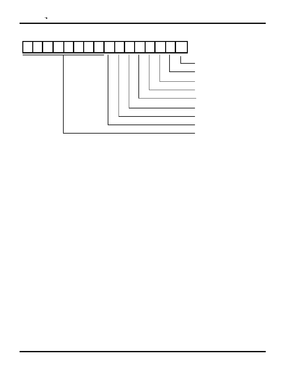
<%
%/15 75% 7PKXGTUCN 5GTKCN %QPVTQNNGT
ZiLOG
&55%%
(KIWTG 4GEGKXG +PVGTTWRV %QPVTQN 4GIKUVGT
&
&
&
&
&
&
&
&
&
&
&
&
&
&
&
&
#FFTGUU
6%4 4GCF %QWPV6%
4Z 1XGTTWP +#
2CTKV[ 'TTQT(TCOG #DQTV +#
5VCVWU QP 9QTFU
4Z %8'16'1( +#
4Z $TGCM#DQTV +#
4Z +FNG +#
'ZKVGF *WPV +#
4Z (+(1 %QPVTQN CPF 5VCVWU
(KNN+PVGTTWRV&/# .GXGN
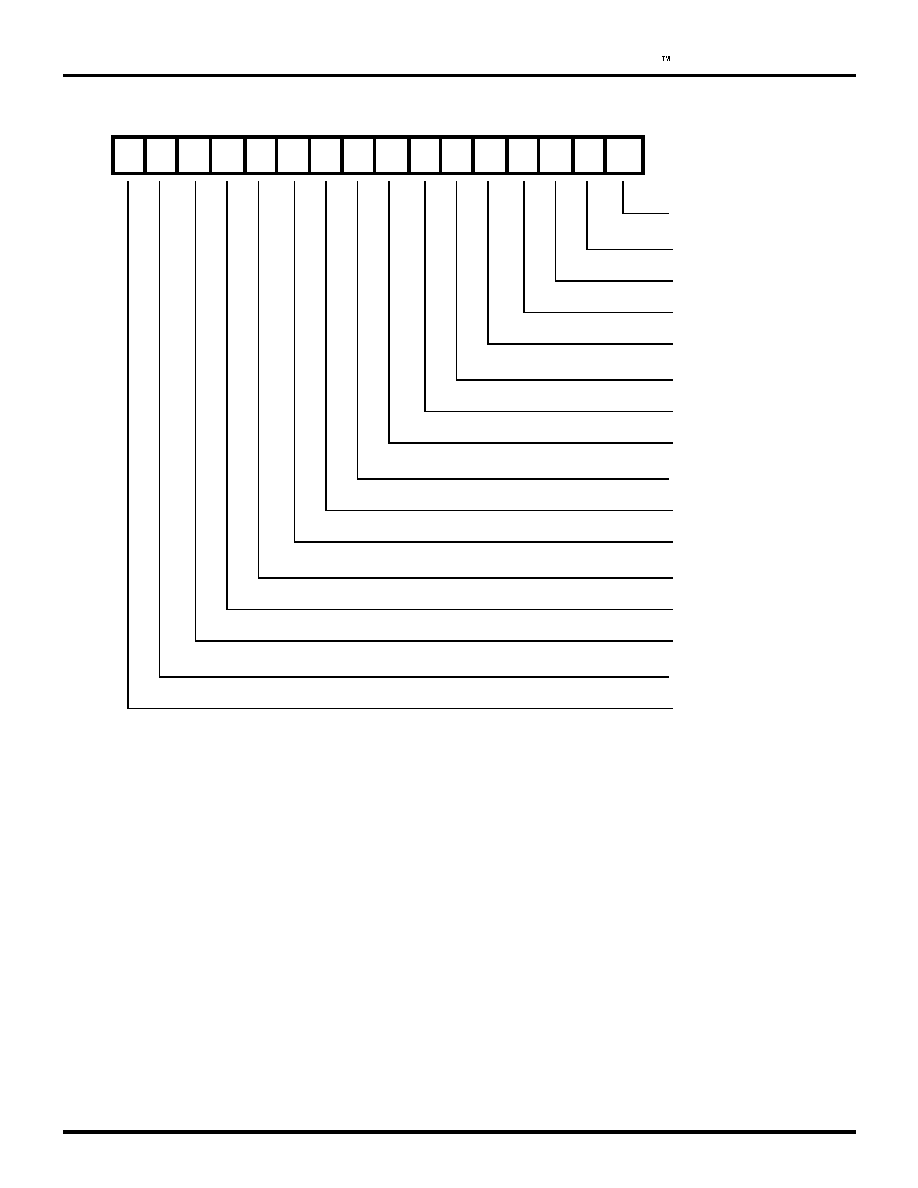
<%
ZiLOG
%/15 75% 7PKXGTUCN 5GTKCN %QPVTQNNGT
&55%%
(KIWTG 4GEGKXG 5[PE 4GIKUVGT
&
&
&
&
&
&
&
&
&
&
&
&
&
&
&
&
#FFTGUU
45;0
45;0
45;0
45;0
45;0
45;0
45;0
45;0
45;0
45;0
45;0
45;0
45;0
45;0
45;0
45;0
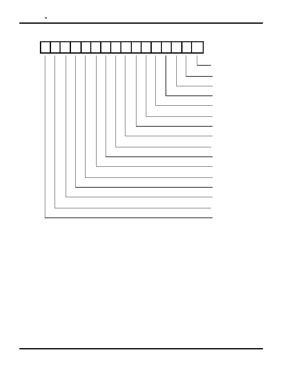
<%
%/15 75% 7PKXGTUCN 5GTKCN %QPVTQNNGT
ZiLOG
&55%%
(KIWTG 4GEGKXG %QWPV .KOKV 4GIKUVGT
&
&
&
&
&
&
&
&
&
&
&
&
&
&
&
&
#FFTGUU
4%.
4%.
4%.
4%.
4%.
4%.
4%.
4%.
4%.
4%.
4%.
4%.
4%.
4%.
4%.
4%.

<%
ZiLOG
%/15 75% 7PKXGTUCN 5GTKCN %QPVTQNNGT
&55%%
(KIWTG 4GEGKXG %JCTCEVGT %QWPV 4GIKUVGT
&
&
&
&
&
&
&
&
&
&
&
&
&
&
&
&
#FFTGUU
4%%
4
4%%
4
4%%
4
4%%
4
4%%
4
4%%
4
4%%
4
4%%
4
4%%
4
4%%
4
4%%
4
4%%
4
4%%
4
4%%
4
4%%
4
4%%
4
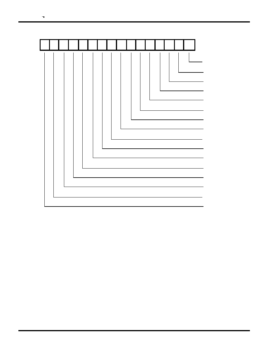
<%
%/15 75% 7PKXGTUCN 5GTKCN %QPVTQNNGT
ZiLOG
&55%%
(KIWTG 6KOG %QPUVCPV 4GIKUVGT
&
&
&
&
&
&
&
&
&
&
&
&
&
&
&
&
#FFTGUU
6%
6%
6%
6%
6%
6%
6%
6%
6%
6%
6%
6%
6%
6%
6%
6%
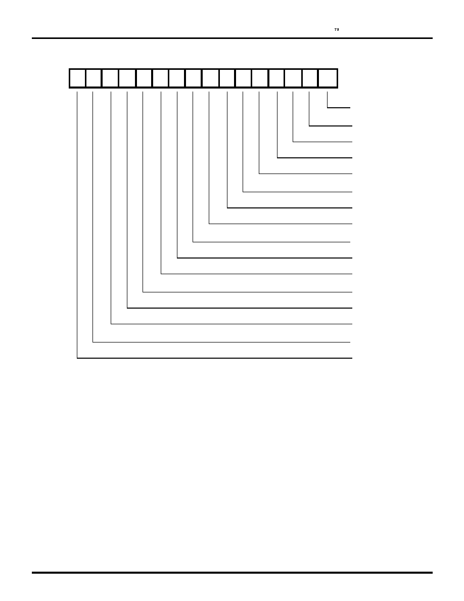
<%
ZiLOG
%/15 75% 7PKXGTUCN 5GTKCN %QPVTQNNGT
&55%%
(KIWTG 6TCPUOKV &CVC 4GIKUVGT
&
&
&
&
&
&
&
&
&
&
&
&
&
&
&
&
#FFTGUU Z
6Z
9
6Z
9
6Z
9
6Z
9
6Z
9
6Z
9
6Z
9
6Z
9
6Z
9
6Z
9
6Z
9
6Z
9
6Z
9
6Z
9
6Z
9
6Z
9
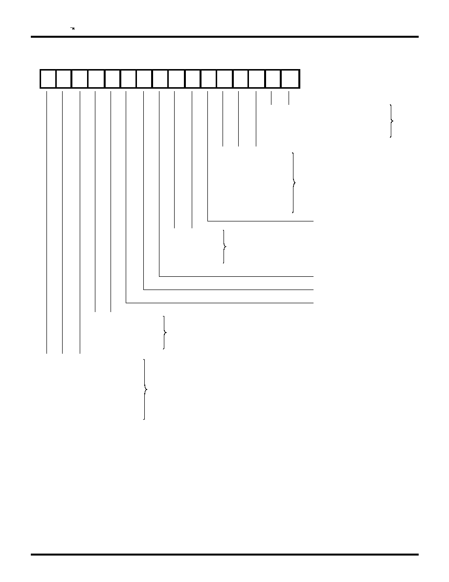
<%
%/15 75% 7PKXGTUCN 5GTKCN %QPVTQNNGT
ZiLOG
&55%%
(KIWTG 6TCPUOKV /QFG 4GIKUVGT
&
&
&
&
&
&
&
&
&
&
&
&
&
&
&
&
#FFTGUU
&KUCDNG +OOGFKCVGN[
&KUCDNG #HVGT 4GEGRVKQP
'PCDNG 9KVJQWV #WVQ'PCDNGU
'PCDNG 9KVJ #WVQ'PCDNG
6Z
'PCDNG
$KVU
$KV
$KVU
$KVU
$KVU
$KVU
$KVU
$KVU
4Z %JCTCEVGT
.GPIVJ
'XGP
1FF
5RCEG
/CTM
6Z 2CTKV[
5GPUG
%4%%%+66
%4%
%4%
4GUGTXGF
6Z %4%
2QN[PQOKCN
04<
04<$
04<+/CTM
04<+5RCEG
$KRJCUG/CTM
$KRJCUG5RCEG
$KRJCUG.GXGN
&KHH $KRJCUG.GXGN
6Z &CVC
&GEQFKPI
6Z %4% QP '1('1/
6Z %4% 'PCDNG
6Z %4% 2TGUGV 8CNWG
6Z 2CTKV[ GPCDNG

<%
ZiLOG
%/15 75% 7PKXGTUCN 5GTKCN %QPVTQNNGT
&55%%
(KIWTG 6TCPUOKV %QOOCPF5VCVWU 4GIKUVGT
&
&
&
&
&
&
&
&
&
&
&
&
&
&
&
&
#FFTGUU
0WNN %QOOCPF
4GUGTXGF
2TGUGV %4%
'PVGT *WPV /QFG
4GUGTXGF
5GNGEV (+(1 5VCVWU
5GNGEV (+(1 +PVGTTWRV .GXGN
5GNGEV (+(1 5VCVWU .GXGN
5GPF (TCOG /GUUCIG
5GPF #DQTV
4GUGTXGF
4GUGTXGF
4GUGV &.' +PJKDKV
5GV &.' +PJKDKV
4GUGV '1('1/
5GV '16'1/
0WNN %QOOCPF
4GUGTXGF
2TGUGV %4%
'PVGT *WPV /QFG
4GUGTXGF
5GNGEV (+(1 5VCVWU
5GNGEV (+(1 +PVGTTWRV .GXGN
5GNGEV (+(1 5VCVWU .GXGN
6Z $WHHGT 'ORV[
4
6Z 7PFGTTWP
#NN 5GPV
4
6Z %4% 5GPV
6Z '1('16 5GPV
6Z #DQTV 5GPV
6Z +FNG 5GPV
6Z 2TGCODNG 5GPV
6Z +FNG .KPG
%QPFKVKQP
6Z 9CKV QP 7PFGTTWP
6TCPUOKV
%QOOCPF
9
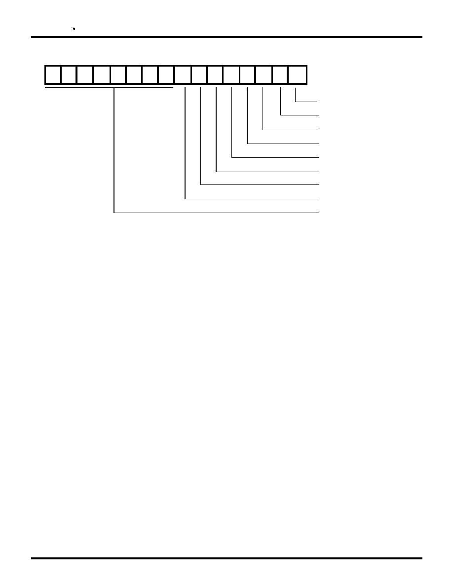
<%
%/15 75% 7PKXGTUCN 5GTKCN %QPVTQNNGT
ZiLOG
&55%%
(KIWTG 6TCPUOKV +PVGTTWRV %QPVTQN 4GIKUVGT
&
&
&
&
&
&
&
&
&
&
&
&
&
&
&
&
#FFTGUU
6%4 4GCF %QWPV6%
6Z 1XGTTWP +#
9CKV HQT 5GPF %QOOCPF
6Z %4% 5GPV +#
6Z '1('16 5GPV +#
6Z #DQTV 5GPV +#
6Z +FNG 5GPV +#
6Z 2TGCODNG 5GPV +#
6Z (+(1 %QPVTQN CPF 5VCVWU
(KNN+PVGTTWRV&/# NGXGN

<%
ZiLOG
%/15 75% 7PKXGTUCN 5GTKCN %QPVTQNNGT
&55%%
(KIWTG 6TCPUOKV 5[PE 4GIKUVGT
&
&
&
&
&
&
&
&
&
&
&
&
&
&
&
&
#FFTGUU
65;0
65;0
65;0
65;0
65;0
65;0
65;0
65;0
65;0
65;0
65;0
65;0
65;0
65;0
65;0
65;0
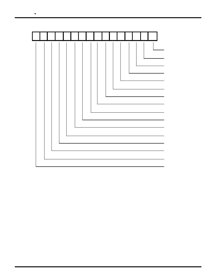
<%
%/15 75% 7PKXGTUCN 5GTKCN %QPVTQNNGT
ZiLOG
&55%%
(KIWTG 6TCPUOKV %QWPV .KOKV 4GIKUVGT
&
&
&
&
&
&
&
&
&
&
&
&
&
&
&
&
#FFTGUU
6%.
6%.
6%.
6%.
6%.
6%.
6%.
6%.
6%.
6%.
6%.
6%.
6%.
6%.
6%.
6%.
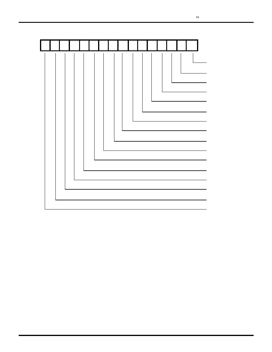
<%
ZiLOG
%/15 75% 7PKXGTUCN 5GTKCN %QPVTQNNGT
&55%%
(KIWTG 6TCPUOKV %JCTCEVGT %QWPV 4GIKUVGT
&
&
&
&
&
&
&
&
&
&
&
&
&
&
&
&
#FFTGUU
6%%
6%%
6%%
6%%
6%%
6%%
6%%
6%%
6%%
6%%
6%%
6%%
6%%
6%%
6%%
6%%
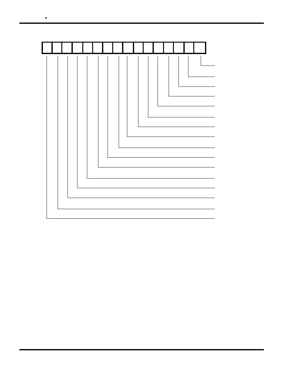
<%
%/15 75% 7PKXGTUCN 5GTKCN %QPVTQNNGT
ZiLOG
&55%%
(KIWTG 6KOG %QPUVCPV 4GIKUVGT
&
&
&
&
&
&
&
&
&
&
&
&
&
&
&
&
#FFTGUU
6%
6%
6%
6%
6%
6%
6%
6%
6%
6%
6%
6%
6%
6%
6%
6%
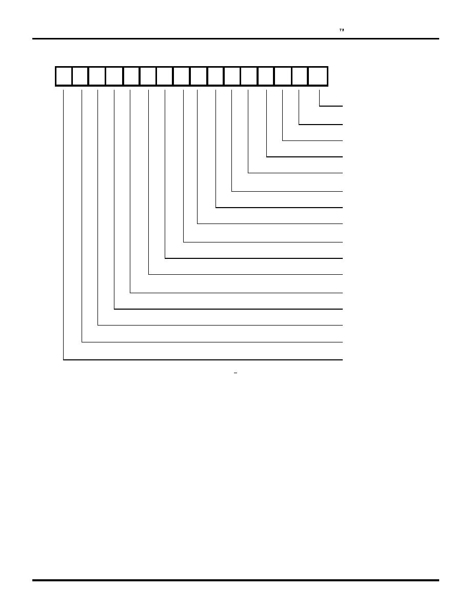
<%
ZiLOG
%/15 75% 7PKXGTUCN 5GTKCN %QPVTQNNGT
&55%%
(KIWTG 4GEGKXG 5VCVWU $NQEM 4GIKUVGT
&
&
&
&
&
&
&
&
&
&
&
&
&
&
&
&
#FFTGUU 0QPG�
4%%
4Z 1XGTTWP
2CTKV[ 'TTQT(TCOG #DQTV
%4% 'TTQT
4Z %8'16'1(
4%% (+(1 1XGTHNQY
5JQTV (TCOG%8 2QNCTKV[
4GUKFWG %QFG
4GUKFWG %QFG
4GUKFWG %QFG
(KTUV $[VG KP 'TTQT
5GEQPF $[VG KP 'TTQT
� 4GHGT VQ (KIWTG %JCPPGN %QPVTQN 4GIKUVGT $KVU HQT #EEGUU /GVJQF

<%
%/15 75% 7PKXGTUCN 5GTKCN %QPVTQNNGT
ZiLOG
&55%%
(KIWTG 6TCPUOKV 5VCVWU $NQEM 4GIKUVGT
(KIWTG $WU %QPHKIWTCVKQP 4GIKUVGT
&
&
&
&
&
&
&
&
&
&
&
&
&
&
&
&
#FFTGUU 0QPG�
� 4GHGT VQ (KIWTG %JCPPGN %QPVTQN 4GIKUVGT $KVU HQT #EEGUU /GVJQF
$KVU
$KV
$KVU
$KVU
$KVU
$KVU
$KVU
$KVU
*&.% 6Z .CUV
%JCTCEVGT .GPIVJ
4GUGTXGF
4GUGTXGF
6Z 5WDOQFG
6Z 5WDOQFG
6Z 5WDOQFG
6Z 5WDOQFG
&
&
&
&
&
&
&
&
&
&
&
&
&
&
&
&
#FFTGUU 0QPG
5JKHV 4KIJV #FFTGUUGU
&QWDNG2WNUG +06#%-
$KV $WU
�
4GUGTXGF
5VCVG #NN 2KPU
5GRCTCVG #FFTGUU HQT $KV $WU
�/WUV DG RTQITCOOGF CU \GTQ
<%
ZiLOG
%/15 75% 7PKXGTUCN 5GTKCN %QPVTQNNGT
&55%%
2#%-#)' +0(14/#6+10
(KIWTG 2KP 2.%% 2CEMCIG &KCITCO
(KIWTG 2KP 83(2 2CEMCIG &KCITCO

<%
%/15 75% 7PKXGTUCN 5GTKCN %QPVTQNNGT
ZiLOG
&55%%
14&'4+0) +0(14/#6+10
For fast results, contact your local ZiLOG sales office for
assistance in ordering the part desired.
%1&'5
©1999 by ZiLOG, Inc. All rights reserved. Information in this
publication concerning the devices, applications, or technology
described is intended to suggest possible uses and may be
superseded. ZiLOG, INC. DOES NOT ASSUME LIABILITY
FOR OR PROVIDE A REPRESENTATION OF ACCURACY
OF THE INFORMATION, DEVICES, OR TECHNOLOGY
DESCRIBED IN THIS DOCUMENT. ZiLOG ALSO DOES
NOT ASSUME LIABILITY FOR INTELLECTUAL
PROPERTY INFRINGEMENT RELATED IN ANY
MANNER TO USE OF INFORMATION, DEVICES, OR
TECHNOLOGY DESCRIBED HEREIN OR OTHERWISE.
Except with the express written approval of ZiLOG, use of
information, devices, or technology as critical components of
life support systems is not authorized. No licenses are conveyed,
implicitly or otherwise, by this document under any intellectual
property rights.
ZiLOG, Inc.
910 East Hamilton Avenue, Suite 110
Campbell, CA 95008
Telephone (408) 558-8500
FAX (408) 558-8300
Internet:
http://www.zilog.com
<%
/*\
2KP 2.%%
<%85%
2CEMCIG
8 2NCUVKE .GCFGF %JKR %CTTKGT
6GORGTCVWTG
5 u% VQ
u%
5RGGF
/*\
'PXKTQPOGPVCN
% 2NCUVKE 5VCPFCTF
'ZCORNG
< % 8 5 %
KU C <% /*\ 2.%%
∞
VQ
∞
% 2NCUVKE 5VCPFCTF (NQY
'PXKTQPOGPVCN (NQY
6GORGTCVWTG
2CEMCIG
5RGGF
2TQFWEV 0WODGT
<K.1) 2TGHKZ