
1
Z53C80 SCSI
Z
ILOG
PS97SCC0200
FEATURES
P
RODUCT
S
PECIFICATION
Z53C80
S
MALL
C
OMPUTER
S
YSTEM
I
NTERFACE
(SCSI)
s
Asynchronous Interface (Supports 3 MB/s)
s
Direct SCSI Bus Interface with On-Board 48 mA Drivers
s
Supports Target and Initiator Roles
s
Meets SCSI Protocol as Defined in ANSI X3.131-1986
Standard
s
Added "Glitch Eater" Enhancement to Minimize Bus
Reflection
Æ
Apple Macintosh is a registered trademark of Apple Computer, Inc.
s
Pin Compatible with the Industry Standard 5380
s
44-Pin PLCC or 48-Pin DIP Package Styles
s
DMA or Programmed I/O Data Transfers
s
Arbitration Support
s
Supports Normal or Block Mode DMA
s
Memory or I/O Mapped CPU Interface
GENERAL DESCRIPTION
The Z53C80 SCSI (Small Computer System Interface)
controller is designed to implement the SCSI protocol as
defined by the ANSI X3.131-1986 standard, and it is fully
compatible with the industry standard 5380. The device is
capable of operating both as a Target and as an Initiator.
Special high-current open-drain outputs enable it to directly
interface to the SCSI bus. The Z53C80 has the necessary
interface hook-ups which allow the system CPU to
communicate with it as with any other peripheral device.
The CPU can read from, or write to, the SCSI registers
which are addressed as standard or memory-mapped
I/Os.
The Z53C80 increases the system performance by
minimizing the CPU intervention in DMA operations which
the SCSI controls. The CPU is interrupted by the SCSI
when it detects a bus condition that requires attention. It
also supports arbitration and reselection. The Z53C80 has
the proper handshake signals to support normal and block
mode DMA operations with most DMA controllers available.
The added enhancement known as the "Glitch Eater" is
used to minimize effects of bus reflection on improperly
terminated SCSI bus applications. The high frequency
reflections that can occur on the SCSI bus are filtered out,
reducing the sensitivity of the inputs, specifically /REQ and
/ACK to bus signal reflections. Figure 1 shows a worst case
input waveform (labeled A), along with the filtered input
(labeled B) and the output of a Schmitt trigger used to
provide the hysteresis required on SCSI inputs (labeled
C). This enhancement is a requirement for the device to
function properly in a Apple Macintosh
Æ
environment.
Notes:
All Signals with a preceding front slash, "/", are active Low, e.g.,
B//W (WORD is active Low); /B/W (BYTE is active Low, only).
Power connections follow conventional descriptions below:
Connection
Circuit
Device
Power
V
CC
V
DD
Ground
GND
V
SS

2
Z53C80 SCSI
PS97SCC0200
Z
ILOG
GENERAL DESCRIPTION
(Continued)
0
20.0
40.0
60.0
80.0
100.0
120.0
140.0
160.0
180.0
5.50
5.00
4.50
4.00
3.50
3.00
2.50
2.00
1.50
1.00
.50
0
-.50
C
C
C
A
B
A
A
A
A
B
A&B
B
B
Figure 1. Worst Case Unfiltered Input (A), Filtered Input (B),
Output of Schmitt-Trigger Used to Provide Hysteresis (C).

3
Z53C80 SCSI
Z
ILOG
PS97SCC0200
48 mA SCSI Transceivers
Interface
Control
Logic
Data
Input
Register
Data
Output
Register
DMA
Logic
Interrupt
Logic
Control
Registers
CPU BUS
Interface
/IOR
/IOW
/CS
/RESET
A2-A0
D7-D0
/DACK
/EOP
DRQ
READY
IRQ
/DB7-/DB0,
/DBP
/ACK
/ATN
/BSY
/MSG
I//O
C//D
/REQ
/RST
/SEL
Figure 2a. SCSI Block Diagram
D7-D0
A2-A0
/IOR
/IOW
/CS
/RESET
/DACK
/EOP
DRQ
READY
IRQ
GND
/DB7-/DB0, /DBP
/ACK
/ATN
/BSY
/MSG
I//O
C//D
/REQ
/RST
/SEL
VCC
Z53C80
SCSI
Figure 2b. SCSI Pin Functions
4
Z53C80 SCSI
PS97SCC0200
Z
ILOG
GENERAL DESCRIPTION
(Continued)
Figure 4. 44-Pin PLCC Pin Assignments
/IOW
/IOR
D7
D6
D5
VDD
D4
D3
D2
D1
D0
/A
TN
/SEL
/BSY
GND
/DB7
/DB6
/DB5
GND
/DB4
/DB3
/RST
6
Z53C80
SCSI
/RESET
IRQ
DRQ
/EOP
/DACK
GND
READY
A0
A1
A2
/CS
/DB2
/DB1
/DB0
/DBP
/REQ
/ACK
I//O
GND
C//D
/MSG
5
4
3
2
1
44 43 42 41 40
18 19 20 21 22 23 24 25 26 27 28
7
8
9
10
11
12
13
14
15
16
17
GND
39
38
37
36
35
34
33
32
31
30
29
Figure 3. 48-Pin DIP Pin Assignments
/DB7
/RST
GND
/BSY
GND
READY
A0
A1
A2
N/C
/CS
/IOW
/DB6
/DB5
GND
/DB4
/DB3
/DB2
N/C
/DB1
/DB0
GND
/DBP
/REQ
/ACK
I//O
GND
C//D
/MSG
N/C
D0
D1
/SEL
/ATN
N/C
/RESET
IRQ
DRQ
/EOP
/DACK
1
2
3
4
5
6
7
8
9
10
11
12
13
14
15
16
17
18
19
20
48
47
46
45
44
43
42
41
40
39
38
37
36
35
34
33
32
31
30
29
Z53C80
SCSI
/IOR
D7
D6
D5
D2
D3
D4
VCC
21
22
23
24
28
27
26
25

5
Z53C80 SCSI
Z
ILOG
PS97SCC0200
PIN DESCRIPTION
Microprocessor Bus
A2-A0
Address Lines (Input).
Address lines are used to
access all internal registers with /CS, /IOR, and /IOW.
/CS
/Chip Select (Input, active Low). /CS, in conjunction
with /RD or /WR, enables the internal register selected by
A2-A0, to be read from or write to. /CS and /DACK must
never be active simultaneously.
/DACK
/DMA Acknowledge (Input, active Low). /DACK, in
conjunction with /IOR and /IOW, is used to enable reading
or writing the SCSI I/O Data Registers when in the DMA
Mode. When the DRQ has acknowledged that the byte has
been successfully transferred to or from the DMA controller,
this signal is asserted. /DACK and /CS must never be
active simultaneously.
DRQ
DMA Request (Output, active High). This signal is
asserted when the chip is ready to transfer a data byte to
and from the DMA controller. The DMA Request will be
asserted only if the DMA Mode bit (Register 2, Bit 1) is set.
The transfer is complete upon reception of /DACK.
D7-D0
Data Lines (Bi-directional; Tri-State, active High).
The Data Bus lines carry data and commands to and from
SCSI. D7 is the most significant bit of this bus.
/EOP
/End of Process (Input, active Low). To terminate a
DMA transfer, this signal is asserted. The current byte will
be transferred but no additional bytes will be requested if
asserted during a DMA cycle. /EOP can be used to
generate an interrupt when it is received from a DMA
Controller.
/IOR
/I/O Read (Input, active Low). This signal is used to
read an internal register selected by /CS and A2-A0. The
Input Data Register can also be selected by this signal
when /DACK is active during DMA transfers.
/IOW
/I/O Write (Input, active Low). This signal is used to
write to an internal register selected by /CS and A2-A0. The
Output Data Register can also be selected by this signal
when used with /DACK during DMA transfers.
IRQ
Interrupt Request (Output, active High). IRQ alerts the
microprocessor of an error condition or an event completion.
Most of the interrupts are individually maskable.
READY
Ready (Output, active High). This signal can be
used to control the data transfer handshaking of block
mode DMA transfers. READY is asserted to indicate that
the chip is ready to transfer data and remains false after a
transfer until the chip is ready for another DMA transfer.
READY is always asserted when the DMA Mode Bit is a
zero.
/RESET
/Reset (Input, active Low). /RESET clears all
registers and has no effect upon the SCSI /RST signal.
Therefore it does not reset the SCSI bus.

6
Z53C80 SCSI
PS97SCC0200
Z
ILOG
SCSI BUS
The following signals are all Bi-directional, active Low,
open-drain, with 48 mA sink capacity. All pins interface
directly with the SCSI Bus.
/ACK
/Acknowledge (Bi-directional, Open-Drain, Active
Low). /ACK is driven by the Initiator and indicates an
acknowledgment for a SCSI data transfer. /ACK is received
as a response to the /REQ Signal in the Target role.
/ATN
/Attention (Bi-directional, Open-Drain, Active Low).
/ATN is driven by the Initiator and indicates an attention
condition. /ATN is received and is responded to by entering
the Message Out Phase in the Target role.
/BSY
/Busy (Bi-directional, Open-Drain, Active Low). /BSY
indicates that the SCSI Bus is being occupied. /BSY can be
driven by both the Target and the Initiator device.
/C//D
/Control//Data (Bi-directional, Open-Drain, Active
Low).
/C//D indicates Control or Data information is on the
SCSI Bus. This signal is driven by a Target and is received
by the Initiator.
/I//O
/Input//Output (Bi-directional, Open-Drain, Active Low).
/I//O is driven by a Target and controls the direction of data
transfer on the SCSI Bus. When asserted, this signal
indicates input to the Initiator. When not asserted, this
signal indicates output from the Initiator. This signal is also
used to recognize the difference between the Selection
and Reselection Phases.
/MSG
/Message (Bi-directional, Open-Drain, Active Low).
The Target drives /MSG active during the Message Phase
and is received by the Initiator.
/REQ
/Request (Bi-directional, Open-Drain, Active Low).
Received by the Initiator and driven by a Target, /REQ
indicates a request for an SCSI data-transfer handshake.
/RST
SCSI Bus RESET (Bi-directional, Open-Drain, Active
Low). The /RST signal shows a SCSI Bus RESET condition
has occurred.
/DB7-/DB0,/DBP
/Data Bits, /Parity Bits (Bi-directional,
Open-Drain, Active Low). These eight data bits (/DB7-/
DB0), plus a parity bit (/DBP) form the SCSI Data Bus. /DB7
has the highest priority during the Arbitration phase and is
the most significant bit (MSB). Data parity is odd and is
always generated and optionally checked, which is not
valid during Arbitration.
/SEL
/Select (Bi-directional, Open-Drain, Active Low).
/SEL is used by a Target to select an Initiator, or by an
Initiator to reselect a Target.

7
Z53C80 SCSI
Z
ILOG
PS97SCC0200
FUNCTIONAL DESCRIPTION
General.
The Small Computer System interface (SCSI)
device has a set of eight registers that are controlled by the
CPU. By reading and writing the appropriate registers, the
CPU may initiate any SCSI Bus activity or may sample and
assert any signal on the SCSI Bus. This allows the user to
implement all or any of the SCSI protocol in software. These
registers are read (written) by activating /CS with an
address on A2-A0 and then issuing a /RD (/WR) pulse. This
section describes the operation of the internal registers
(Table 1).
Table 1. Register Summary
Address
A2
A1
A0
R/W
Register Name
0
0
0
R
Current SCSI Data
0
0
0
W
Output Data
0
0
1
R/W
Initiator Command
0
1
0
R/W
Mode
0
1
1
R/W
Target Command
1
0
0
R
Current SCSI Bus Status
1
0
0
W
Select Enable
1
0
1
R
Bus and Status
1
0
1
W
Start DMA Send
1
1
0
R
Input Data
1
1
0
W
Start DMA Target Receive
1
1
1
R
Reset Parity/Interrupt
1
1
1
W
Start DMA Initiator Receive
Data Registers.
The data registers are used to transfer
SCSI commands, data, status, and message bytes between
the microprocessor Data Bus and the SCSI Bus. The SCSI
does not interpret any information that passes through the
data registers. The data registers consist of the transparent
Current SCSI Data Register, the Output Data Register, and
the Input Data Register.
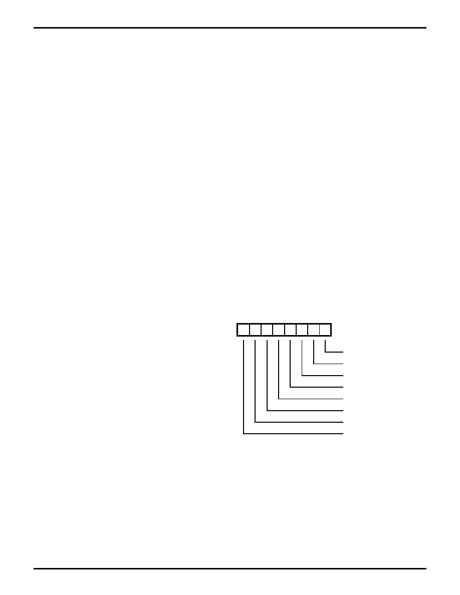
Current SCSI Data Register.
Address 0 (Read Only). The
Current SCSI Data Register (Figure 5) is a read-only
register which allows the microprocessor to read the active
SCSI Data Bus. This is accomplished by activating /CS
with an address on A2-A0 and issuing a /RD pulse. If parity
checking is enabled, the SCSI Bus parity is checked at the
beginning of the read cycle. This register is used during a
programmed I/O data read or during Arbitration to check
for higher priority arbitrating devices. Parity is not
guaranteed valid during Arbitration.
Figure 5. Current SCSI Data Register
Output Data Register.
Address 0 (Write Only). The Output
Data Register (Figure 6) is a write-only register that is used
to send data to the SCSI Bus. This is accomplished by
either using a normal CPU write, or under DMA control, by
using /WR and /DACK. This register also asserts the
proper ID bits on the SCSI Bus during the Arbitration and
Selection phases.
/DB0
/DB1
/DB2
/DB3
/DB4
/DB5
/DB6
/DB7
Address: 0
(Read Only)
D7 D6 D5 D4 D3 D2 D1 D0
/DB0
/DB1
/DB2
/DB3
/DB4
/DB5
/DB6
/DB7
D7 D6 D5 D4 D3 D2 D1 D0
Address: 0
(Write Only)
Figure 6. Output Data Register
8
Z53C80 SCSI
PS97SCC0200
Z
ILOG
FUNCTIONAL DESCRIPTION
(Continued)
Input Data Register.
Address 6 (Read Only). The input
Data Register (Figure 7) is a read-only register that is used
to read latched data from the SCSI Bus. Data is latched
either during a DMA Target receive operation when /ACK
goes active or during a DMA Initiator receive when /REQ
goes active. The DMA Mode bit (Mode Register bit 1) must
be set before data can be latched in the Input Data
Register. This register is read under DMA control using
/RD and /DACK. Parity is optionally checked when the
Input Data Register is loaded.
Assert Data Bus
Assert /ATN
Assert /SEL
Assert /BSY
Assert /ACK
Lost Arbitration
Arbitration in Progress
Assert /RST
Address: 1
(Read Only)
D7 D6 D5 D4 D3 D2 D1 D0
Figure 8. Initiator Command Register
(Register Read)
/DB0
/DB1
/DB2
/DB3
/DB4
/DB5
/DB6
/DB7
Address: 6
(Read Only)
D7 D6 D5 D4 D3 D2 D1 D0
Figure 7. Input Data Register
Initiator Command Register.
Address 1 (Read/Write).
The Initiator Command Register (Figures 8 and 9) are read
and write registers which assert certain SCSI Bus signals,
monitors those signals, and monitors the progress of bus
arbitration. Many of these bits are significant only when
being used as an Initiator; however, most can be used
during Target role operation.
Assert Data Bus
Assert /ATN
Assert /SEL
Assert /BSY
Assert /ACK
"0"
Test Mode
Assert /RST
Address: 1
(Write Only)
D7 D6 D5 D4 D3 D2 D1 D0
Figure 9. Initiator Command Register
(Register Write)

9
Z53C80 SCSI
Z
ILOG
PS97SCC0200
The following paragraphs describe the operation of all bits
in the Initiator Command Register.
Bit 0.
Assert Data Bus. The Assert Data Bus bit, when set,
allows the contents of the Output Data Register to be
enabled as chip outputs on the signals /DB7-/DB0. Parity
is also generated and asserted on /DBP.
When connected as an Initiator, the outputs are only
enabled if the Target Mode bit (Mode Register, bit 6) is
False, the received signal I//O is False, and the phase
signals C//D, I//O, and /MSG match the contents of the
Assert C//O, Assert I//O and Assert /MSG in the Target
Command Register.
This bit should also be set during DMA send operations.
Bit 1.
Assert/ATN/. Bit 1 may be asserted on the SCSI Bus
by setting this bit to a 1 if the Target Mode bit (Mode
Register, bit 6) is False, /ATN is normally asserted by the
initiator to request a Message Out bus phase. Note that
since Assert/SEL and Assert/ATN are in the same register,
a select with /ATN may be implemented with one CPU write
/ATN may be deasserted by resetting this bit to zero. A
read on this register simply reflects the status of this bit.
Bit 2.
Assert/SEL. Writing a 1 into this bit position asserts
/SEL onto the SCSI Bus. /SEL is normally asserted after
Arbitration has been successfully completed /SEL may be
disabled by resetting bit 2 to a 0. A read of this register
reflects the status of this bit.
Bit 3.
Assert/BSY. Writing a 1 into this bit position asserts
/BSY onto the SCSI Bus. Conversely, a 0 resets the /BSY
signal. Asserting /BSY indicates a successful selection or
reselection. Resetting this bit creates a Bus-Disconnect
condition. Reading this register reflects bit status.
Bit 4.
Assert/ACK. Bit 4 is used by the bus initiator to assert
/ACK on the SCSI Bus. In order to assert /ACK, the Target
Mode bit (Mode Register, bit 6) must be False. Writing a
zero to this bit deasserts /ACK. Reading this register
reflects bit status.
Bit 5.
"0" (Write Bit). Bit 5 should be written with a 0 for
proper operation.
Bit 5.
LA (Lost Arbitration - Read Bit). Bit 5, when active,
indicates that the SCSI detected a Bus-Free condition,
arbitrated for use of the bus by asserting /BSY and its ID on
the Data Bus, and lost Arbitration due to /SEL being
asserted by another bus device. This bit is active only
when the Arbitrate bit (Mode Register, bit 0) is active.
Bit 6.
Test Mode (Write Bit). Bit 6 is written during a test
environment to place all output drivers, in the high
impedance state.
Bit 6.
AIP (Arbitration in Process - Read Bit). Bit 6 is used
to determine if Arbitration is in progress. For this bit to be
active, the Arbitrate bit (Mode Register, bit 0) must have
been set previously. It indicates that a Bus-Free condition
has been detected and that the chip has asserted /BSY
and put the contents of the Output Data Register onto the
SCSI Bus. AIP will remain active until the Arbitrate bit is
reset.
Bit 7.
Assert/RST. Whenever a one is written to bit 7 of the
Initiator Command Register, the /RST signal is asserted on
the SCSI Bus. The /RST signal will remain asserted until this
bit is reset or until an external /RESET occurs. After this bit
is set (1), IRQ goes active and all internal logic and control
registers are reset (except for the interrupt latch and the
Assert/RST bit). Writing a zero to bit 7 of the Initiator
Command Register deasserts the /RST signal. The status
of this bit is monitored by reading the Initiator Command
Register.
Mode Register.
Address 2 (Read/Write). The Mode
Register controls the operation of the chip. This register
determines whether the SCSI operates as an Initiator or a
Target, whether DMA transfers are being used, whether
parity is checked, and whether interrupts are generated on
various external conditions. This register is read to check
the value of these internal control bits (Figure 10).
Arbitrate
DMA Mode
Monitor /BSY
Enable /EOP Interrupt
Enable Parity Interrupt
Enable Parity Checking
Target Mode
"0"
Address: 2
(Read/Write)
D7 D6 D5 D4 D3 D2 D1 D0
Figure 10. Mode Register

10
Z53C80 SCSI
PS97SCC0200
Z
ILOG
FUNCTIONAL DESCRIPTION
(Continued)
Bit 0.
Arbitrate. The Arbitrate bit is set (1) to start the
Arbitration process. Prior to setting this bit, the Output Data
Register should contain the proper SCSI device ID value.
Only one data bit should be active for SCSI Bus Arbitration.
The SCSI waits for a Bus-Free condition before entering
the Arbitration phase. The results of the Arbitration phase
is determined by reading the status bits LA and AIP
(Initiator Command Register, bits 5 and 6, respectively).
Bit 1.
DMA Mode. The DMA Mode bit is normally used to
enable a DMA transfer and must be set (1) prior to writing
Start DMA Send Register, Start DMA Target Receive
Register, and Start DMA Initiator Receiver Register. These
three registers are used to start DMA transfers. The Target
Mode bit (Mode Register, bit 6) must be consistent with
writes to Start DMA Target Receive and Start DMA Initiator
Receive Registers [i.e., set (1) for a write to start DMA
Target Receive Register and set (0) for a write to Start DMA
Initiator Receive Register]. The control bit Assert Data Bus
(Initiator Command Register, bit 0) must be True (1) for all
DMA send operations. In the DMA mode, /REQ and /ACK
are automatically controlled.
The DMA Mode bit is not reset upon the receipt of an /EOP
signal. Any DMA transfer is stopped by writing a zero into
this bit location; however, care must be taken not to cause
/CS and /DACK to be active simultaneously.
Bit 2.
Monitor Busy. The Monitor Busy bit, when True (1),
causes an interrupt to be generated for an unexpected
loss of /BSY. When the interrupt is generated due to loss of
/BSY, the lower six bits of the Initiator Command Register
are reset (0) and all signals are removed from the SCSI
Bus.
Bit 3.
Enable/EOP interrupt. The enable /EOP interrupt,
when set (1), causes an interrupt to occur when the /EOP
(End of Process) signal is received from the DMA controller
logic.
Bit 4.
Enable Parity Interrupt. The Enable Parity Interrupt
bit, when set (1), will cause an interrupt (IRQ) to occur if a
parity error is detected. A parity interrupt will only be
generated if the Enable Parity Checking bit (bit 5) is also
enabled (1).
Bit 5.
Enable Parity Checking. The Enable Parity Checking
bit determines whether parity errors are ignored or saved
in the parity error latch. If this bit is reset (0), parity is
ignored. Conversely, if this bit is set (1), parity errors are
saved.
Bit 6.
Targetmode. The Targetmode bit allows the SCSI to
operate as either a SCSI Bus Initiator, bit reset (0), or as a
SCSI Bus Target device, bit set (1). If the signals /ATN and
/ACK are to be asserted on the SCSI Bus, the Targetmode
bit must be reset (0). If the signals C//D, I//O, /MSG, and
/REQ are to be asserted on the SCSI Bus, the Targetmode
bit must be set (1).
Bit 7.
0. Bit 7 should be written with a zero for proper
operation.
Target Command Register.
Address 3 (Read/Write). When
connected as a target device, the Target Command
Register (Figure 11) allows the CPU to control the SCSI Bus
Information Transfer phase and/or to assert /REQ by writing
this register. The Targetmode bit (Mode Register, bit 6)
must be True (1) for bus assertion to occur. The SCSI Bus
phases are described in Table 2.
Table 2. SCSI Information Transfer Phase
Bus Phase
ASSERT
ASSERT
ASSERT
I//O
C//D
/MS
Data Out
0
0
0
Unspecified
0
0
1
Command
0
1
0
Message Out
0
1
1
Data In
1
0
0
Unspecified
1
0
1
Status
1
1
0
Message In
1
1
1
When connected as an Initiator with DMA Mode True, if the
phase lines I//O, C//D, and /MSG do not match the phase
bits in the Target Command Register, a phase mismatch
interrupt is generated when /REQ goes active. To send
data as an Initiator, the Assert I//O, Assert C//D, and Assert
/MSG bits must match the corresponding bits in the Current
SCSI Bus Status Register. The Assert /REQ bit (bit 3) has
no meaning when operating as an Initiator.
Bits 4, 5, and 6 are not used.
11
Z53C80 SCSI
Z
ILOG
PS97SCC0200
Bit 7.
Last Byte Sent (Read Only). The End Of DMA
Transfer bit (Bus and Status Register, bit 7) only indicates
when the last byte was received from the DMA controller.
The Last Byte Sent bit can be used to flag that the last byte
of the DMA send operation has been transferred on the
SCSI Data Bus.
/DBP
/SEL
I//O
C//D
/MSG
/REQ
/BSY
/RST
Address: 4
(Read Only)
D7 D6 D5 D4 D3 D2 D1 D0
/DB0
/DB1
/DB2
/DB3
/DB4
/DB5
/DB6
/DB7
Address: 4
(Write Only)
D7 D6 D5 D4 D3 D2 D1 D0
Assert I//O
Assert C//D
Assert /MSG
Assert /REQ
"X"
Last Byte Sent
Address: 3
(Read/Write)
D7 D6 D5 D4 D3 D2 D1 D0
Figure 11. Target Command Register
Current SCSI Bus Status Register.
Address 4 (Read
Only). The Current SCSI Bus Register is a read-only
register which is used to monitor seven SCSI Bus control
signals, plus the Data Bus parity bit. For example, an
Initiator device can use this register to determine the
current bus phase and to poll /REQ for pending data
transfers. This register may also be used to determine why
a particular interrupt occurred. Figure 12 describes the
Current SCSI Bus Status Register.
Select Enable Register.
Address 4 (Write Only). The
Select Enable Register (Figure 13) is a write-only register
which is used as a mask to monitor a signal ID during a
selection attempt. The simultaneous occurrence of the
correct ID bit, /BSY FALSE, and /SEL TRUE will cause an
interrupt. This interrupt can be disabled by resetting all bits
in this register. If the Enable Parity Checking bit (Mode
Register, bit 5) is active (1), parity is checked during
selection.
Figure 12. Current SCSI Bus Status Register
Figure 13. Select Enable Register

12
Z53C80 SCSI
PS97SCC0200
Z
ILOG
FUNCTIONAL DESCRIPTION
(Continued)
Bus and Status Register.
Address 5 (Read Only). The
Bus and Status Register (Figure 14) is a read-only register
which can be used to monitor the remaining SCSI control
signals not found in the Current SCSI Bus Status Registers
(/ATN and /ACK), as well as six other status bits. The
following describes each bit of the Bus Status Register
individually.
Bit 0.
/ACK. Bit 0 reflects the condition of the SCSI Bus
control signal /ACK. This signal is normally monitored by
the Target device.
Bit 1.
/ATN. Bit 1 reflects the condition of the SCSI Bus
control signal /ATN. This signal is normally monitored by
the Target device.
Bit 4.
Interrupt Request Active. Bit 4 is set if an enabled
interrupt condition occurs. It reflects the current state of the
IRQ output and can be cleared by reading the Reset Parity/
Interrupt Register.
Bit 5.
Parity Error. Bit 5 is set if a parity error occurs during
a data receive or a device selection. The Parity Error bit can
only be set (1) if the Enable Parity Check bit (Mode
Register, bit 5) is active (1). This bit may be cleared by
reading the Reset Parity/Interrupt Register.
Bit 6.
DMA Request. The DMA Request bit allows the CPU
to sample the output pin DRQ. DRQ can be cleared by
asserting /DACK or by resetting the DMA MODE bit (bit 1)
in the Mode Register. The DRQ signal does not reset when
a phase-mismatch interrupt occurs.
Bit 7.
End Of DMA Transfer. The End Of DMA Transfer bit
is set if /EOP, /DACK, and either /RD or /WR are
simultaneously active for at least 100 ns. Since the /EOP
signal can occur during the last byte sent to the Output
Data Register, the /REQ and /ACK signals should be
monitored to ensure that the last byte has been transferred.
This bit is reset when the DMA MODE bit is reset (0) in the
Mode Register.
DMA Registers.
Three write-only registers are used to
initiate all DMA activity. They are: Start DMA Send, Start
DMA Target Receive, and Start DMA Initiator Receive.
Performing a write operation into one of these registers
starts the desired type of DM transfer. Data presented to
the SCSI on signals D7-D0 during the register write is
meaningless and has no effect on the operation. Prior to
writing these registers, the DMA Mode bit (bit 1), and the
Target mode bit (bit 6) in the Mode Register must be
appropriately set. The individual registers are briefly
described as follows:
Start DMA Send.
Address 5 (Write Only). This register is
written to initiate a DMA send, from the DMA to the SCSI
Bus, for either Initiator or Target role operations. The DMA
Mode bit (Mode Register, bit 1) is set prior to writing this
register.
Start DMA Target Receive.
Address 6 (Write Only). This
register is written to initiate a DMA receive - from the SCSI
Bus to the DMA, for Target operation only. The DMA Mode
bit (bit 1) and the Targetmode bit (bit 6) in the Mode
Register must both be set (1) prior to writing this register.
/ACK
/ATN
Busy Error
Phase Match
Interrupt Request Active
Parity Error
DMA Request
End of DMA
Address: 5
(Read Only)
D7 D6 D5 D4 D3 D2 D1 D0
Figure 14. Bus and Status Register
Bit 2.
Busy Error. The Busy Error bit is active if an unexpected
loss of the /BSY signal has occurred. This latch is set
whenever the Monitor Busy bit (Mode Register, bit 2) is
True and /BSY is False. An unexpected loss of /BSY
disables any SCSI outputs and resets the DMA Mode bit
(Mode Register, bit 1).
Bit 3.
Phase Match. The SCSI signals /MSG, C//D, and
I//O, represent the current information transfer phase. The
Phase Match bit indicates whether the current SCSI Bus
phase matches the lower three bits of the Target Command
Register. Phase Match is continuously updated and is only
significant when operating as a Bus Initiator. A phase
match is required for data transfers to occur on the SCSI
Bus.
13
Z53C80 SCSI
Z
ILOG
PS97SCC0200
Start DMA Initiator Receive.
Address 7 (Write Only). This
register is written to initiate a DMA receive from the SCSI
Bus to the DMA, for Initiator operation only. The DMA Mode
bit (bit 6) must be False (0) in the Mode Register prior to
writing this register.
Reset Parity/Interrupt.
Address 7 (Read Only). Reading
this register resets the Parity Error bit (bit 5), the Interrupt
Request bit (bit 4), and the Busy Error bit (bit 2) in the Bus
and Status Register.
On-Chip SCSI Hardware Support.
The SCSI is easy to
use because of its simple architecture. The chip allows
direct control and monitoring of the SCSI Bus by providing
a latch for each signal. However, portions of the protocol
define timings which are much too quick for traditional
microprocessors to control. Therefore, hardware support
has been provided for DMA transfers, bus arbitration,
phase change monitoring, bus disconnection, bus reset,
parity generation, parity checking, and device selection/
reselection.
Arbitration is accomplished using a Bus-Free filter to
continuously monitor /BSY. If /BSY remains inactive for at
least 400 ns, the SCSI is considered free and Arbitration
may begin. Arbitration will begin if the bus is free, /SEL is
inactive, and the Arbitrate bit (Mode Register, bit 0) is
active. Once arbitration has begun (/BSY asserted), an
arbitration delay of 2.2
µ
s must elapse before the Data Bus
can be examined to determine if Arbitration is enabled.
This delay is implemented in the controlling software
driver.
The Z53C80 is a clockwise device. Delays such as bus-
free delay, bus-set delay, and bus-settle delay are
implemented using gate delays. These delays may differ
between devices because of inherent process variations,
but are well within the proposed ANSI X3.131 - 1986
specification.
Interrupts.
The Z53C80 provides an interrupt output (IRQ)
to indicate a task completion or an abnormal bus
occurrence. The use of interrupts is optional and may be
disabled by resetting the appropriate bits in the Mode
Register or the Select Enable Register.
When an interrupt occurs, the Bus and Status Register and
the Current SCSI Bus Status Register (Figures 12 and 14)
must be read to determine which condition created the
interrupt. IRQ can be reset simply by reading the Reset
Parity/Interrupt Register or by an external chip reset
/RESET active for 100 ns.
Assuming the Z53C80 has been properly initialized, an
interrupt will be generated if the chip is selected or
reselected, if an /EOP signal occurs, if a parity error occurs
during a data transfer, if a bus phase mismatch occurs, or
if a SCSI Bus disconnection occurs.
Selection Reselection.
The Z53C80 generates a select
interrupt if SEL is active (0), its device ID is True and /BSY
is False for at least a bus-settle delay. If I//O is active, this
is considered a reselect interrupt. The correct ID bit is
determined by a match in the Select Enable Register. Only
a single bit match is required to generate an interrupt. This
interrupt may be disabled by writing zeros into all bits of the
Select Enable Register.
If parity is supported, parity should be good during the
selection phase. Therefore, if the Enable Parity bit (Mode
Register, bit 5) is active, the Parity Error bit is checked to
ensure that a proper selection has occurred. The Enable
Parity Interrupt bit need not be set for this interrupt to be
generated.
The proposed SCSI specification also requires that no
more than two device IDs be active during the selection
process. To ensure this, the Current SCSI Data Register is
read.
The proper values for the Bus and Status Register and the
Current SCSI Bus Status Register are displayed in Figures
15 and 16, respectively.
/ACK
/ATN
Busy Error
Phase Match
Interrupt Request Active
Parity Error
DMA Request
End of DMA
0
0
0
1
X
0
X
0
D7
D0
Figure 15. Bus and Status Register

14
Z53C80 SCSI
PS97SCC0200
Z
ILOG
FUNCTIONAL DESCRIPTION
(Continued)
Figure 16. Current SCSI Bus Status Register
End of Process (EOP) Interrupt.
An End Of Process
signal (EOP) which occurs during a DMA transfer (DMA
Mode True) will set the End of DMA Status bit (Bus and
Status Register bit 7) and will optionally generate an
interrupt if Enable EOP Interrupt bit (Mode Register, bit 3)
is True. The /EOP pulse will not be recognized (End of DMA
bit set) unless /EOP, /DACK, and either /RD or /WR are
concurrently active for at least 50 ns. DMA transfers can
still occur if /EOP was not asserted at the correct time. This
interrupt is disabled by resetting the Enable EOP Interrupt
bit.
The proper values for the Bus and Status Register and the
Current SCSI Bus Status Register for this interrupt are
shown in Figures 17 and 18.
Figure 17. Bus and Status Register
Figure 18. Current SCSI Bus Status Register
The End of DMA bit is used to determine when a block
transfer is complete. Receive operations are complete
when there is no data left in the chip and no additional
handshakes occurring. The only exception to this is
receiving data as an Initiator and the Target opts to send
additional data for the same phase. In this /REQ goes
active and the new data is present in the Input Data
Register. Since a phase-mismatch interrupt will not occur,
/REQ and /ACK need to be sampled to determine that the
Target is attempting to send more data.
For send operations, the End of DMA bit is set when the
DMA finishes its transfers, but the SCSI transfer may still be
in progress. If connected as a Target, /REQ and /ACK
should be sampled until both are False. If connected as an
Initiator, a phase change interrupt is used to signal the
completion of the previous phase. It is possible for the
Target to request additional data for the same phase. In
this case, a phase change will not occur and both /REQ
and /ACK are sampled to determine when the last byte was
transferred.
SCSI Bus Reset.
The SCSI generates an interrupt when
the /RST signal transitions to True. The device releases all
bus signals within a bus-clear delay of this transition. This
interrupt also occurs after setting the Assert /RST bit
(Initiator Command Register, bit 7). This interrupt cannot
be disabled. (Note: /RST is not latched in bit 7 of the
Current SCSI Bus Status Register and is not active when
this port is read. For this case, the Bus Reset interrupt is
determined by default.)
The proper values for the Bus and Status Register and the
Current SCSI Bus Status Register are displayed in Figures
19 and 20, respectively.
D7
D0
/DBP
/SEL
I//O
C//D
/MSG
/REQ
/BSY
/RST
0
0
0
X
X
X
0
X
D7
D0
/ACK
/ATN
Busy Error
Phase Match
Interrupt Request Active
Parity Error
DMA Request
End of DMA
1
0
0
1
0
0
0
X
D7
D0
/DBP
/SEL
I//O
C//D
/MSQ
/REQ
/BSY
/RST
0
1
1
X
X
X
0
X

15
Z53C80 SCSI
Z
ILOG
PS97SCC0200
D7
D0
/ACK
/ATN
Busy Error
Phase Match
Interrupt Request Active
Parity Error
DMA Request
End of DMA
0
X
1
1
1
0
X
X
Figure 19. Bus and Status Register
Figure 20. Current SCSI Bus Status Register
Parity Error.
An interrupt is generated for a received parity
error it the Enable Parity Check (bit 5) and the Enable Parity
Interrupt (bit 4) bits are set (1) in the Mode Register. Parity
is checked during a read of the Current SCSI Data Register
and during a DMA receive operation. A parity error can be
detected without generating an interrupt by disabling the
Enable Parity Interrupt bit and checking the Parity Error
flag (Bus and Status Register, bit 5).
The proper values for the Bus and Status Register and the
Current SCSI Bus Status Register are displayed in Figures
21 and 22, respectively.
Figure 21. Bus and Status Register
Figure 22. Current SCSI Bus Status Register
Bus Phase Mismatch.
The SCSI phase lines have the
signals I//O, C//D, and /MSG. These signals are compared
with the corresponding bits in the Target Command
Register: Assert I//O (bit 0), Assert C//D (bit 1), and Assert
/MSG (bit 2). The comparison occurs continually and is
reflected in the Phase Match bit (bit 3) of the Bus and Status
Register. If the DMA Mode bit (Mode Register, bit 1) is
active and a phase mismatch occurs when /REQ transitions
from False to True, an interrupt (IRQ) is generated.
D7
D0
/ACK
/ATN
Busy Error
Phase Match
Interrupt Request Active
Parity Error
DMA Request
End of DMA
0
X
0
1
X
0
X
X
D7
D0
/DBP
/SEL
I//O
C//D
/MSG
/REQ
/BSY
/RST
X
X
X
X
X
X
X
X
D7
D0
/DBP
/SEL
I//O
C//D
/MSQ
/REQ
/BSY
/RST
0
1
1
X
X
X
0
X

16
Z53C80 SCSI
PS97SCC0200
Z
ILOG
FUNCTIONAL DESCRIPTION
(Continued)
A phase mismatch prevents the recognition of /REQ and
removes the chip from the bus during an Initiator send
operation (/DB7-/DB0 and /DBP will not be driven even
through the Assert Data Bus bit (Initiator Command Register,
bit 0). This may be disabled by resetting the DMA Mode bit
(Note: It is possible for this interrupt to occur when
connected as a Target if another device is driving the
phase lines to a different state).
The proper values for the Bus and Status Register and the
Current SCSI Bus Status Register are displayed in Figures
23 and 24, respectively.
Loss of BSY.
If the Monitor Busy bit (bit 2) in the Mode
Register is active, an interrupt is generated if the BSY
signal goes FALSE for at least a bus-settle delay. This
interrupt is disabled by resetting the Monitor Busy bit.
Register values are displayed in Figures 25 and 26.
Figure 25. Bus and Status Register
Figure 26. Current SCSI Bus Status Register
Figure 23. Bus and Status Register
Figure 24. Current SCSI Bus Status Register
D7
D0
/DBP
/SEL
I//O
C//D
/MSQ
/REQ
/BSY
/RST
0
0
0
X
X
X
0
0
D7
D0
/ACK
/ATN
Busy Error
Phase Match
Interrupt Request Active
Parity Error
DMA Request
End of DMA
0
0
0
1
0
0
X
0
D7
D0
/ACK
/ATN
Busy Error
Phase Match
Interrupt Request Active
Parity Error
DMA Request
End of DMA
0
0
0
1
X
1
0
0
D7
D0
/DBP
/SEL
I//O
C//D
/MSQ
/REQ
/BSY
/RST
0
1
X
X
X
X
0
X

17
Z53C80 SCSI
Z
ILOG
PS97SCC0200
Reset Conditions.
Three possible reset situations exist
with the Z53C80, as follows:
Hardware Chip Reset.
When the signal RST is active for
at least 100 ns, the Z53C80 device is re-initialized and all
internal logic and control registers are cleared. This is a
chip reset only and does not create a SCSI Bus-Reset
condition.
SCSI Bus Reset (/RST) Received.
When a SCSI /RST
signal is received, an IRQ interrupt is generated and a chip
reset is performed. All internal logic and registers are
cleared, except for the IRQ interrupt latch and the Assert
/RST bit (bit 7) in the Initiator Command Register. (Note:
The /RST signal may be sampled by reading the Current
SCSI Bus Status Register, however, this signal is not
latched and may not be present when this port is read.)
SCSI Bus Reset (/RST) Issued.
If the CPU sets the Assert
/RST bit+ 7) in the Initiator Command Register, the /RST
signal goes active on the SCSI Bus and an internal reset is
performed. Again, all internal logic and registers are
cleared except for the IRQ interrupt latch and the Assert
/RST bit (bit 7) in the Initiator Command Register. The /RST
signal will continue to be active until the Assert /RST bit is
reset or until a hardware reset occurs.
Data Transfers.
Data is transferred between SCSI Bus
devices in one of four modes: 1) Programmed I/O, 2)
Normal DMA, 3) Block Mode DMA, or 4) Pseudo DMA. The
following sections describe these modes in detail (Note:
for all data transfer operations /DACK and /CS should
never be active simultaneously.)
Programmed I/O Transfers.
Programmed I/O is the most
primitive form of data transfer. The /REQ and /ACK
handshake signals are individually monitored and asserted
by reading and writing the appropriate register bits. This
type of transfer is normally used when transferring small
blocks of data such as command blocks or message and
status bytes. An Initiator send operation would begin by
setting the C//D, I//O, and /MSG bits in the Target Command
Register to the correct state so that a phase match exists.
In addition to the phase match condition, it is necessary for
the Assert Data Bus bit (Initiator Command Register, bit 0)
to be True and the received I/O signal to be False for the
Z53C80 to send data. For each transfer, the data is loaded
into the Output Data Register. The CPU then waits for the
/REQ bit (Current SCSI Bus Status Register, bit 5) to
become active. Once /REQ goes active, the Phase Match
bit (Initiator Command Register, bit 4) is set. The /REQ bit
is sampled until it becomes FALSE and the CPU resets the
Assert /ACK bit to complete the transfer.
Normal DMA Mode.
DMA transfers are normally used for
large block transfers. The SCSI chip outputs a DMA
request (DRQ) whenever it is ready for a byte transfer.
External DMA logic uses this DRQ signal to generate
/DACK and a /RD or a /WR pulse to the Z53C80. DRQ goes
inactive when /DACK is asserted and /DACK goes inactive
some time after the minimum read or write pulse width.
This process is repeated for every byte. For this mode,
/DACK should not be allowed to cycle unless a transfer is
taking place.
Block Mode Transfers.
The Block Mode DMA transfers
allow an external DMA controller, such as the Intel 8237,
to perform successive DMA transfers without abandoning
the data bus to the microprocessor. Keeping an active
/DACK prevents the (Intel-type) CPUs from gaining control
of the system bus. The Block Mode handshaking method
does not increase the transfer rate. Preventing the CPU
from multiplexing the system bus does not have any
speed advantages. Therefore, this is not recommended
for initiator use.
In the Block Mode, the SCSI chip asserts the DRQ signal
to initiate the transfer. The DMA controller responds to the
DRQ signal by asserting the /DACK and remains asserted
throughout the transfer. The 53C80 asserts the READY
signal after the /IOR or /IOW signals deassert, effectively
replacing the DRQ signal. The READY signal for Intel-type
DMA controllers extends the memory read and write
signals. Therefore, D7-D0 is available to be read or written
on the system bus until the SCSI chip is ready for the next
transfer. This transfer method prevents the CPU from
executing any action, such as a refresh cycle on the
system bus. In the non-block DMA mode, the system bus
is unoccupied until the 53C80 asserts DRQ. This indicates
that the chip is ready for the next byte transfer. The
advantage of this mode is that it allows the CPU to use the
system bus while the 53C80 is transferring data across the
SCSI bus.
Caution must be taken when executing this mode due to
the operation of READY. For example, if a phase mismatch
interrupt occurs, the READY signal will stay inactive and
IRQ will be active. Then, the DMA controller cannot give
the system bus back to the CPU for the 53C80 interrupt to
be serviced since READY remains inactive. READY must
be asserted to continue the bus cycle. Therefore, /EOP
should be used in Block Mode so that the CPU can regain
control of the bus after the last byte has been transferred.
To make READY active again, reset the DMA Mode Bit.
Block Mode transfers are stopped in the same fashion as
in the Block Mode. This is executed by resetting the DMA
Mode Bit or using the /EOP signal. (See the previous
section, Normal DMA Mode, for more information on
stopping a DMA transfer.)

18
Z53C80 SCSI
PS97SCC0200
Z
ILOG
FUNCTIONAL DESCRIPTION
(Continued)
Pseudo DMA Mode.
To avoid monitoring and asserting
the request/acknowledgment handshake signals for
programmed I/O transfers, the system may be designed to
implement a pseudo DMA mode. This mode is implemented
by programming the Z53C80 to operate in the DMA mode,
but using the CPU to emulate the DMA handshake. DRQ
may be detected by polling the DMA Request bit (bit 6) in
the Bus and Status Register, by sampling the signal
through an external port, or by using it to generate a CPU
interrupt. Once DRQ is detected, the CPU can perform a
read or write data transfer. This CPU read/write is externally
decoded to generate the appropriate /DACK and /RD or
/WR signals.
Often, external decoding logic is necessary to generate
the /CS signal. This same logic may be used to generate
/DACK at no extra cost and provide an increased
performance in programmed I/O transfers.
Halting a DMA Operation.
The EOP signal is not the only
way to halt a DMA transfer. A bus phase mismatch or a
reset of the DMA MODE bit (Mode Register, bit 1) can also
terminate a DMA cycle for the current bus phase.
Using the /EOP Signal.
If /EOP is used, it should be
asserted for at least 50 ns while /DACK and /RD or /WR are
simultaneously active. Note, however, that if /RD or /WR is
not active, an interrupt is generated, but the DMA activity
continues. The /EOP signal does not reset the DMA MODE
bit. Since the /EOP signal can occur during the last byte
sent to the Output Data Register, the /REQ and /ACK
signals are monitored to ensure that the last byte has
transferred.
Bus Phase Mismatch Interrupt.
A bus phase mismatch
interrupt is used to halt the transfer if operating as an
Initiator. Using this method frees the host from maintaining
a data length counter and frees the DMA logic from
providing the /EOP signal. If performing an Initiator send
operation, the Z53C80 requires /DACK to cycle before
/ACK goes inactive. Since phase changes cannot occur if
/ACK is active, either /DACK must be cycled after the last
byte is sent or the DMA Mode bit must be reset in order to
receive the phase mismatch interrupt.
Resetting the DMA MODE Bit.
A DMA operation may be
halted at any time simply by resetting the DMA Mode bit.
It is recommended that the DMA Mode bit be reset after
receiving an /EOP or bus phase-mismatch interrupt. The
DMA Mode bit must then be set before writing any of the
start DMA registers for subsequent bus phases.
If resetting the DMA Mode bit is used instead of /EOP for
Target role operation, then care must be taken to reset this
bit at the proper time. If receiving data as a Target device,
the DMA Mode bit must be reset once the last DRQ is
received and before /DACK is asserted to prevent an
additional /REQ from occurring. Resetting this bit causes
DRQ to go inactive. However, the last byte received
remains in the Input Data Register and may be obtained
either by performing a normal CPU read or by cycling
/DACK and /RD. In most cases, /EOP is easier to use when
operating as a Target device.

19
Z53C80 SCSI
Z
ILOG
PS97SCC0200
READ REGISTERS
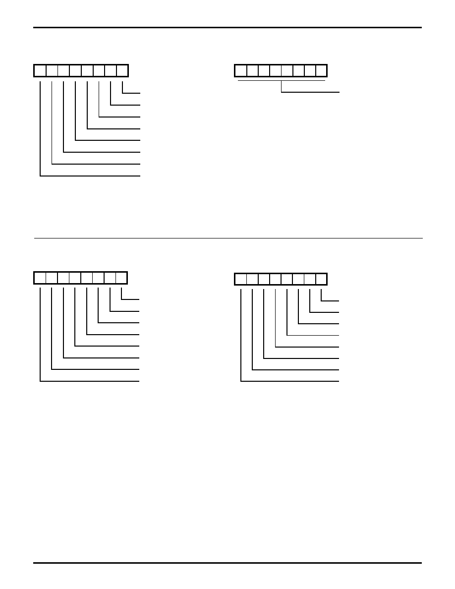
Figure 27. Current SCSI Data Register
Figure 28. Initiator Command Register
Figure 29. Mode Register
Figure 30. Target Command Register
Figure 31. Current SCSI Bus Status Register
Figure 32. Bus and Status Register
/DB0
/DB1
/DB2
/DB3
/DB4
/DB5
/DB6
/DB7
Address: 0
(Read Only)
D7 D6 D5 D4 D3 D2 D1 D0
Assert Data Bus
Assert /ATN
Assert /SEL
Assert /BSY
Assert /ACK
Lost Arbitration
Arbitration in Progress
Assert /RST
Address: 1
(Read Only)
D7 D6 D5 D4 D3 D2 D1 D0
Arbitrate
DMA Mode
Monitor /BSY
Enable /EOP Interrupt
Enable Parity Interrupt
Enable Parity Checking
Target Mode
"0"
Address: 2
(Read Only)
D7 D6 D5 D4 D3 D2 D1 D0
Assert I//O
Assert C//D
Assert /MSG
Assert /REQ
"0"
Last Byte Sent
Address: 3
(Read Only)
D7 D6 D5 D4 D3 D2 D1 D0
/DBP
/SEL
I//O
C//D
/MSG
/REQ
/BSY
/RST
Address: 4
(Read Only)
D7 D6 D5 D4 D3 D2 D1 D0
/ACK
/ATN
Busy Error
Phase Match
Interrupt Request Active
Parity Error
DMA Request
End of DMA
D7 D6 D5 D4 D3 D2 D1 D0
Address: 5
(Read Only)
20
Z53C80 SCSI
PS97SCC0200
Z
ILOG
READ REGISTERS (Continued)
Figure 33. Input Data Register
Figure 34. Reset Parity/Interrupt
WRITE REGISTERS
Figure 35. Output Data Register
Figure 36. Initiator Command Register
/DB0
/DB1
/DB2
/DB3
/DB4
/DB5
/DB6
/DB7
Address: 6
(Read Only)
D7 D6 D5 D4 D3 D2 D1 D0
"X"
Address: 7
(Read Only)
D7 D6 D5 D4 D3 D2 D1 D0
X = Don't Care
/DB0
/DB1
/DB2
/DB3
/DB4
/DB5
/DB6
/DB7
Address: 0
Write Only)
D7 D6 D5 D4 D3 D2 D1 D0
Assert Data Bus
Assert /ATN
Assert /SEL
Assert /BSY
Assert /ACK
"0"
Test Mode
Assert /RST
Address: 1
(Write Only)
D7 D6 D5 D4 D3 D2 D1 D0

21
Z53C80 SCSI
Z
ILOG
PS97SCC0200
Figure 37. Mode Register
Figure 38. Target Command Register
Figure 39. Select Enable Register
Figure 40. Start DMA Send
Figure 41. Start DMA Target Receive
Figure 42. Start DMA Initiator Receive
Arbitrate
DMA Mode
Monitor /BSY
Enable /EOP Interrupt
Enable Parity Interrupt
Enable Parity Checking
Target Mode
"0"
Address: 2
(Write Only)
D7 D6 D5 D4 D3 D2 D1 D0
"X"
Address: 5
(Write Only)
D7 D6 D5 D4 D3 D2 D1 D0
"X"
Address: 7
(Write Only)
D7 D6 D5 D4 D3 D2 D1 D0
Assert I//O
Assert C//D
Assert /MSG
Assert /REQ
"X"
Address: 3
(Write Only)
D7 D6 D5 D4 D3 D2 D1 D0
Last Byte Sent
/DB0
/DB1
/DB2
/DB3
/DB4
/DB5
/DB6
/DB7
Address: 4
(Write Only)
D7 D6 D5 D4 D3 D2 D1 D0
"X"
Address: 6
(Write Only)
D7 D6 D5 D4 D3 D2 D1 D0

22
Z53C80 SCSI
PS97SCC0200
Z
ILOG
ABSOLUTE MAXIMUM RATINGS
Voltages on all pins
with respect to GND ................................. ≠0.3V to +7.0V
Operating Ambient Temperature ...................................
Storage Temperature ............................ ≠65
∞
C to +150
∞
C
Stresses greater than those listed under Absolute Maximum
Ratings may cause permanent damage to this device. This
is a stress rating only; operation of the device at any
condition above those indicated in the operational sections
of these specifications is not implied. Exposure to absolute
maximum rating conditions for extended periods may
affect device reliability.
STANDARD TEST CONDITIONS
The DC characteristics and capacitance section below
apply for the following standard test conditions, unless
otherwise noted. All voltages are referenced to GND.
Positive current flows into the referenced pin. Standard
conditions are as follows:
s
+4.75V
V
CC
+5.25V
s
GND = 0V
s
T
A
as specified in Ordering Information
From Output
Under Test
Threshold
Voltage
75 pF
I = 2 mA
OL
I = 250
µ
A
OH
V = 1.4 V
T
Figure 43. Standard Test Dynamic Load Circuit
Note:
See Ordering Information
+5V
From Output
Under Test
75 pF
2.2 k
Figure 44. Open-Drain Test Load

23
Z53C80 SCSI
Z
ILOG
PS97SCC0200
DC CHARACTERISTICS
Symbol
Parameter
Condition
Min
Max
Units
V
DD
Supply Voltage
4.75
5.25
V
VIH
High-Level Input Voltage
2.0
V
DD
+0.5
V
V
IL
Low-Level Input Voltage
V
SS
≠0.5
0.8
V
I
IH
1
High-Level Input Current
V
IH
= 5.25V
SCSI Bus Pins
V
IL
= 0V
50
µ
A
I
IH
2
High-Level Input Current
V
IH
= 5.25V
All Other Pins
10
µ
A
I
IL
1
Low-Level Input Current
SCSI Bus Pins (Except /RST)
V
IL
= V
SS
≠50
µ
A
I
IL
2
Low-Level Input Current
All Other Pins
V
IL
= V
SS
≠10
µ
A
V
OH
1
High-Level Output Voltage
I
OH
= ≠4 mA
2.4
V
DD
V
V
OL
1
Low-Level Output Voltage
SCSI Bus Pins
I
OL
= 48 mA
V
SS
0.5
V
V
OL
2
Low-Level Output Voltage
All Other Pins
I
OL
= 8 mA
V
SS
0.4
V
I
DD
Supply Current
15
mA
T
A
Operating Free-Air Temperature
0
70
∞
C
24
Z53C80 SCSI
PS97SCC0200
Z
ILOG
AC CHARACTERISTICS
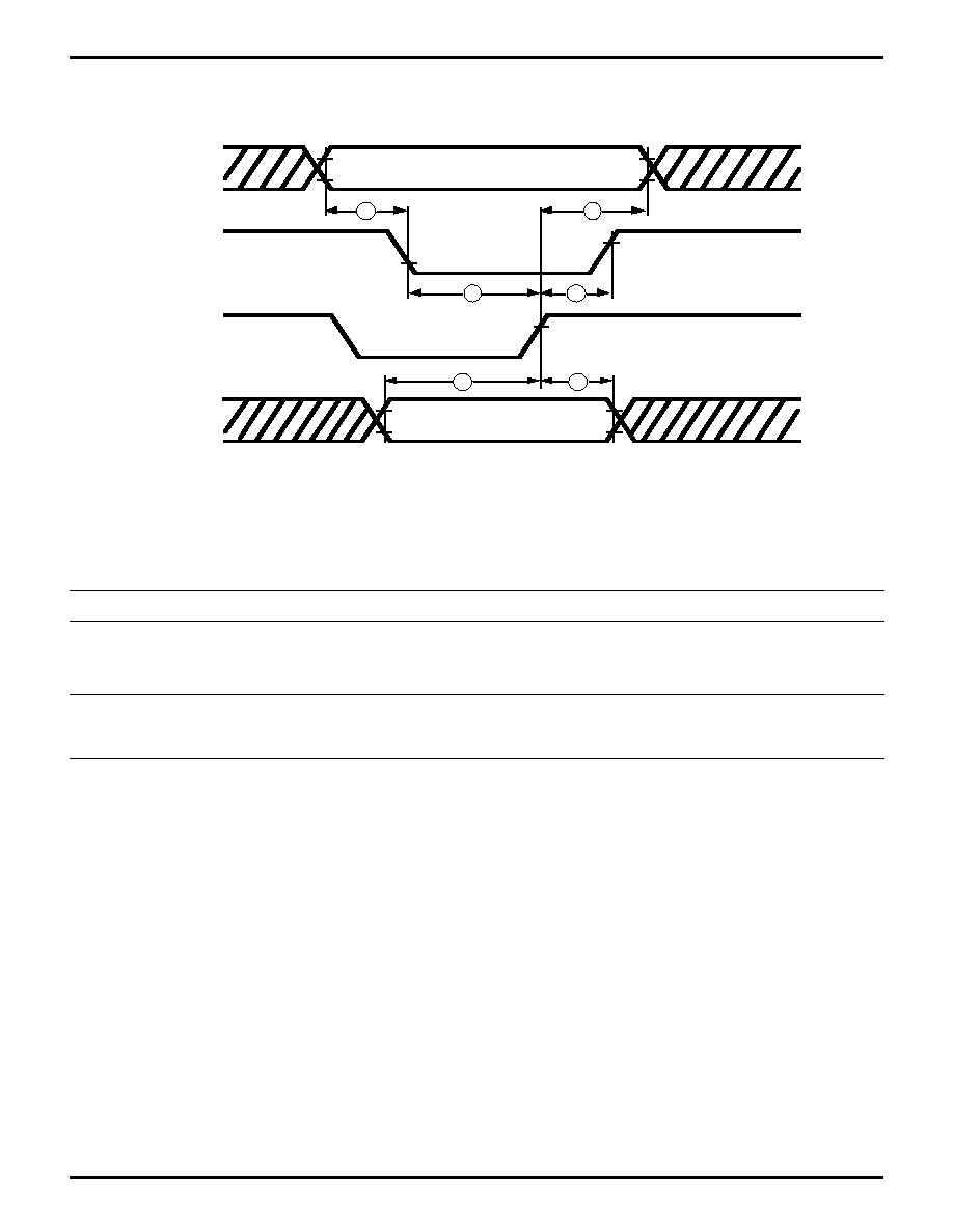
CPU Write Cycle Timing Diagram
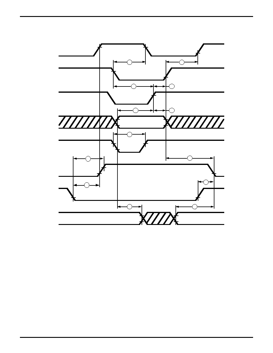
Figure 45. CPU Write Cycle
AC CHARACTERISTICS
CPU Write Cycle Table
No
Description
Min
Max
Units
1
Address Setup to Write Enable
[1]
10
ns
2
Address Hold from End Write Enable
[1]
10
ns
3
Write Enable Width*
40
ns
4
Chip Select Hold from End of /IOW
0
ns
5
Data Setup to end of Write Enable
[1]
20
ns
6
Data Hold Time form End of /IOW
20
ns
Note:
[1] Write Enable is the occurrence of /WR and /CS.
/SCSICS
A2-A0
/RD
D7-D0
1
2
3
4
5
6
25
Z53C80 SCSI
Z
ILOG
PS97SCC0200
AC CHARACTERISTICS
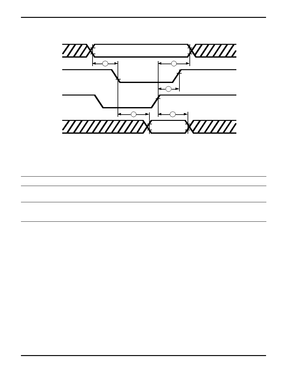
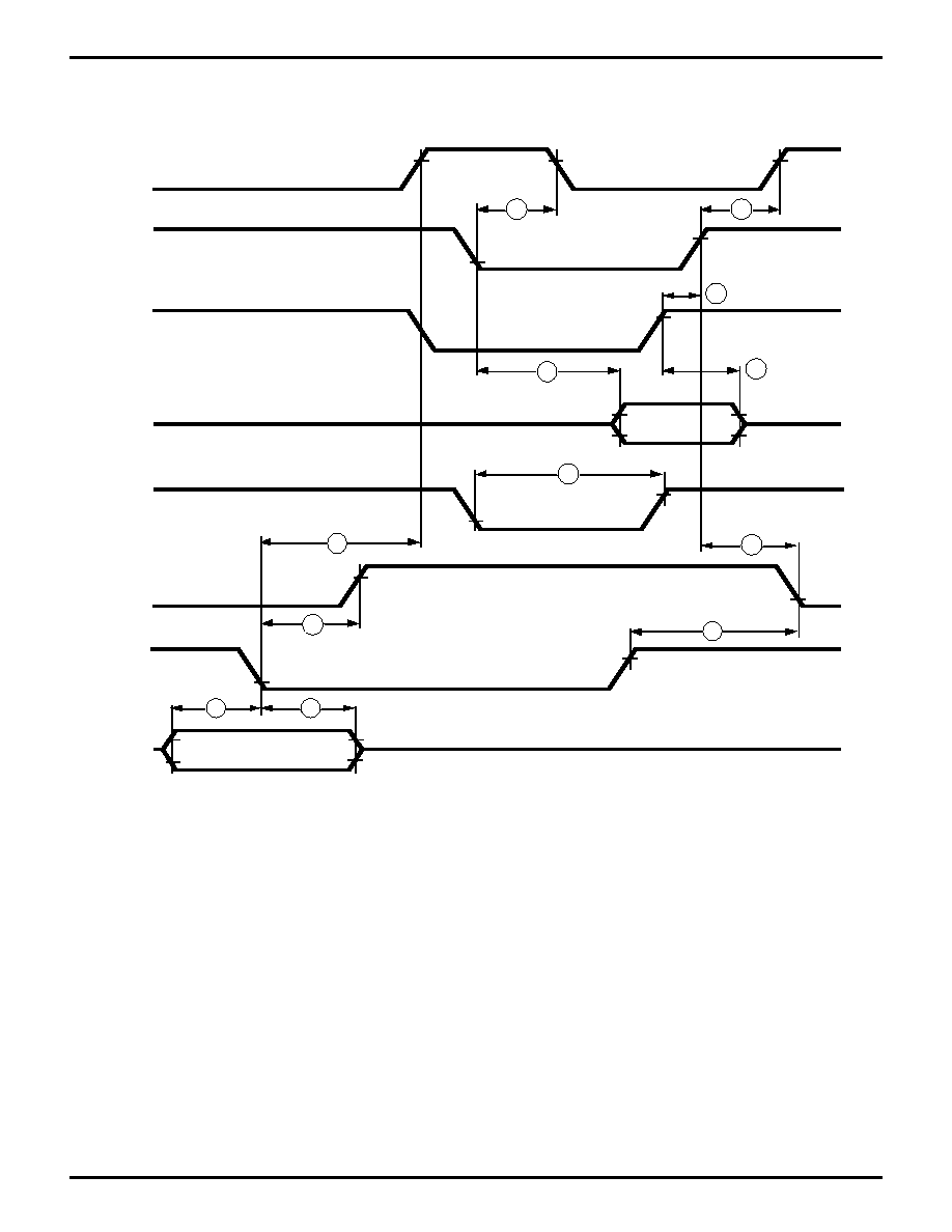
CPU Read Cycle Timing Diagram
A2-A0
/SCSICS
/RD
D7-D0
2
1
3
5
4
Figure 46. CPU Read Cycle
AC CHARACTERISTICS
CPU Read Cycle Table
No
Description
Min
Max
Units
1
Address Setup to Read Enable
[1]
10
ns
2
Address Hold from End Read Enable
[1]
10
ns
3
Chip Select Hold from End of /RD
0
ns
4
Data Access Time from Read Enable
[1]
70
ns
5
Data Hold Time from End of Read Enable
[1]
10
ns
Note:
[1] Read Enable is the occurrence of /RD and /CS.

26
Z53C80 SCSI
PS97SCC0200
Z
ILOG
AC CHARACTERISTICS
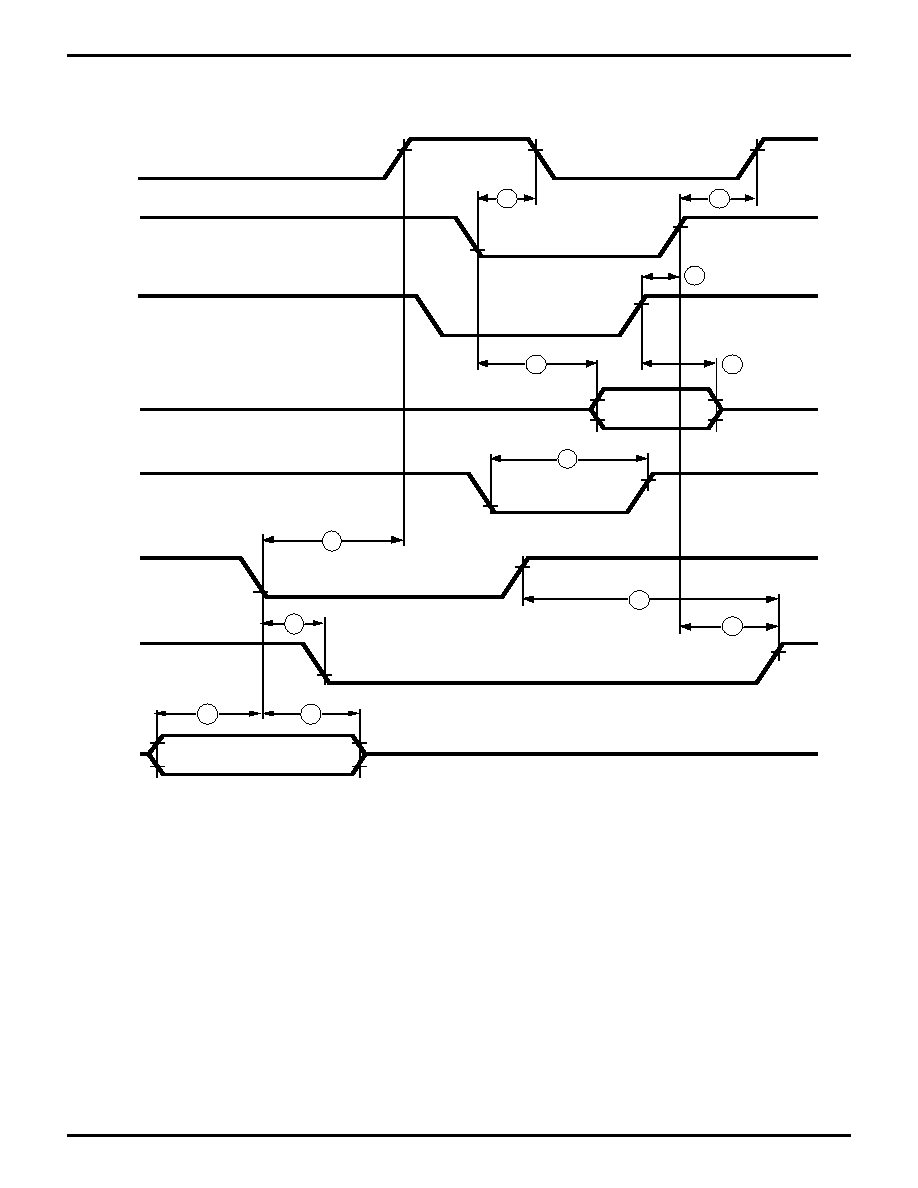
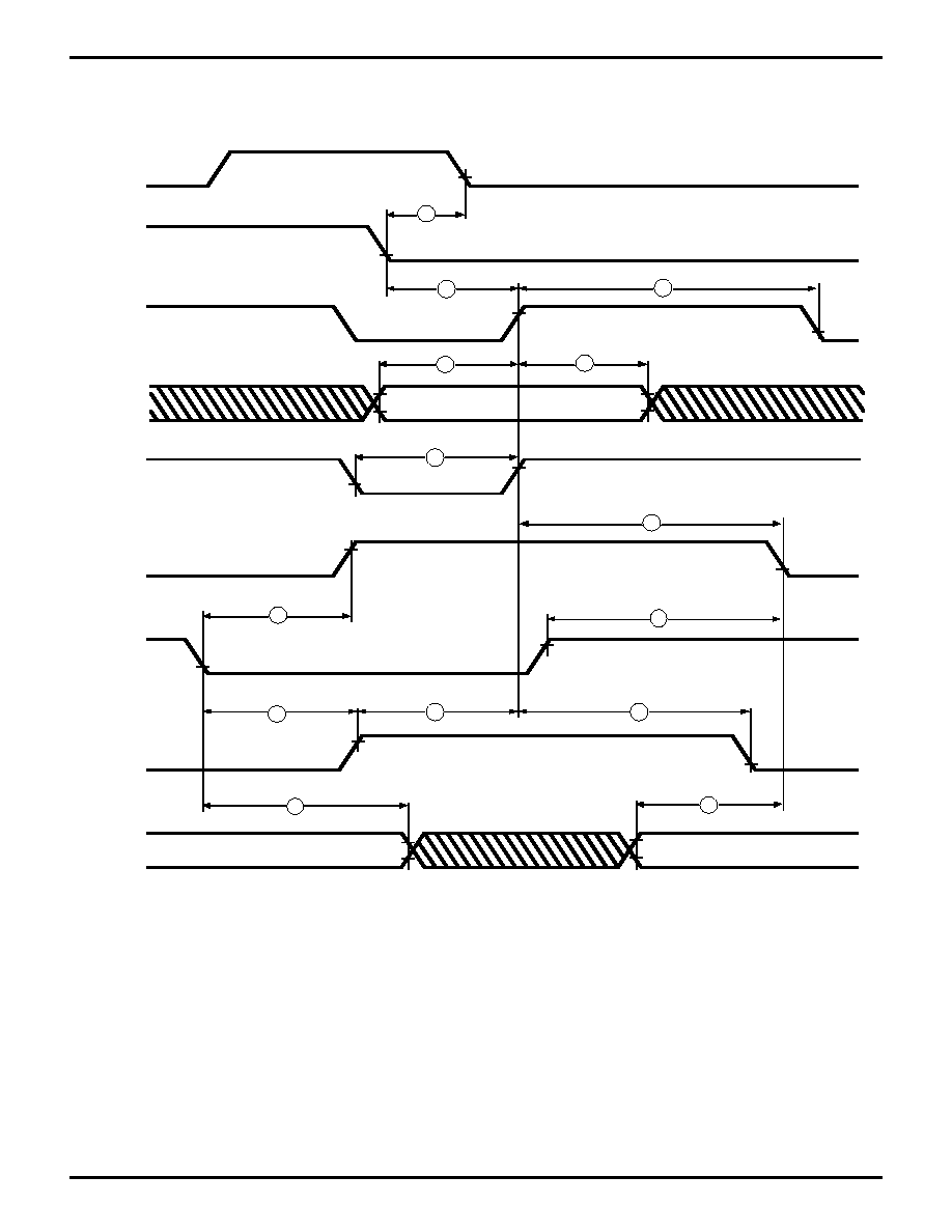
DMA Write (Non-Block Mode) Initiator Send Cycle Timing Diagram
Figure 47. DMA Write (Non-Block Mode) Initiator Send Cycle
DRQ
/DACK
/WR
D7-D0
2
1
9
8
7
3
4
6
5
10
12
11
13
/EOP
/REQ
/ACK
/DB7-/DB0,
/DBP

27
Z53C80 SCSI
Z
ILOG
PS97SCC0200
AC CHARACTERISTICS
DMA Write Initiator Send Cycle Table
No
Description
Min
Max
Units
1
DRQ Low from /DACK Low
60
ns
2
/DACK High to DRQ High
30
ns
3
Write Enable Width
[1]
50
ns
4
/DACK Hold from End of /WR
0
ns
5
Data Setup to End of Write Enable
[1]
50
ns
6
Data Hold Time from End of /WR
25
ns
7
Width of /EOP Pulse
[2]
50
ns
8
/REQ Low to /ACK Low
90
ns
9
/REQ High to DRQ High
70
ns
10
/DACK High to /ACK High
90
ns
11
/WR High to Valid SCSI Data
50
ns
12
Data Hold from Write Enable
[1]
15
ns
13
Data Setup to /ACK Low
55
ns
Notes:
[1]
Write Enable is the occurrence of /WR and /DACK.
[2]
/EOP, /WR, and /DACK must be concurrently Low for at least T7 for
proper recognition of the /EOP pulse.
28
Z53C80 SCSI
PS97SCC0200
Z
ILOG
AC CHARACTERISTICS
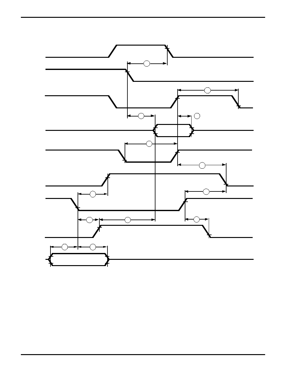
DMA Read (Non-Block Mode) Initiator Receive Timing Diagram
DRQ
/DACK
D7-D0
/EOP
/REQ
/ACK
/DB7-/DB0,
/DBP
/IOR
BYTE N
BYTE N
1
2
3
4
5
6
7
8
9
10
11
12
Figure 48. DMA Read (Non-Block Mode) Initiator Receive

29
Z53C80 SCSI
Z
ILOG
PS97SCC0200
AC CHARACTERISTICS
DMA Read (Non-Block Mode) Initiator Receive Table
Name
Description
Min
Max
Units
1
DRQ False from /DACK True
60
ns
2
/DACK False to DRQ True
30
ns
3
/DACK Hold Time from End of /IOR
0
ns
4
Data Access Time from Read Enable
[1]
70
ns
5
Data Hold Time from End of /IOR
10
ns
6
Width of /EOP Pulse
[2]
50
ns
7
/REQ True to DRQ True
70
ns
8
/REQ True to /ACK True
90
ns
9
/REQ False to /ACK False (/DACK False)
80
ns
10
/DACK False to /ACK False (/REQ False)
90
ns
11
DATA Setup Time to /REQ
20
ns
12
DATA Hold Time from /REQ True
50
ns
Notes:
[1] Read enable is the occurrence of both /IOR and /DACK.
[2] /EOP, /IOR and /DACK must be concurrently true for at least T6 for
proper recognition of the /EOP pulse.
30
Z53C80 SCSI
PS97SCC0200
Z
ILOG
AC CHARACTERISTICS
DMA Write (Non-Block Mode) Target Send Cycle Timing Diagram
6
12
DRQ
/DACK
/WR
D7-D0
/EOP
/REQ
/ACK
/DB7-/DB0,
/DBP
4
13
11
9
1
3
2
7
5
8
10
Figure 49. DMA Write (Non-Block Mode) Target Send Cycle

31
Z53C80 SCSI
Z
ILOG
PS97SCC0200
AC CHARACTERISTICS
DMA Write Target Send Cycle Table
No
Description
Min
Max
Units
1
DRQ Low from /DACK Low
60
ns
2
/DACK High to DRQ High
30
ns
3
Write Enable Width
[1]
50
ns
4
/DACK Hold from /WR High
0
ns
5
Data Setup to End of Write Enable
[1]
50
ns
6
Data Hold Time from End of /WR
25
ns
7
Width of /EOP Pulse
[2]
50
ns
8
/ACK Low to /REQ High
80
ns
9
/REQ from End of /DACK (/ACK High)
90
ns
10
/ACK Low to DRQ High (Target)
70
ns
11
/ACK High to /REQ Low (/DACK High)
100
ns
12
Data Hold from Write Enable
15
ns
13
Data Setup to /REQ Low (Target)
55
ns
Notes:
[1] Write Enable is the occurrence of /IOW and /DACK
[2] /EOP, /WR, and /DACK must be concurrently Low for at least T7 for
proper recognition of the /EOP pulse.
32
Z53C80 SCSI
PS97SCC0200
Z
ILOG
AC CHARACTERISTICS
DMA Read (Non-Block Mode) Target Receive Timing Diagram
DRQ
/DACK
D7-D0
/EOP
/REQ
/ACK
/DB7-/DB0,
/DBP
/IOR
BYTE N
BYTE N
1
2
3
4
5
6
7
8
9
10
12
11
Figure 50. DMA Read (Non-Block Mode) Target Receive

33
Z53C80 SCSI
Z
ILOG
PS97SCC0200
AC CHARACTERISTICS
DMA Read (Non-Block Mode) Target Receive Table
Name
Description
Min
Max
Units
1
DRQ False from /DACK True
60
ns
2
/DACK False to DRQ True
30
ns
3
/DACK Hold Time from End of /IOR
0
ns
4
Data Access Time from Read Enable
[1]
70
ns
5
Data Hold Time from End of /IOR
10
ns
6
Width of /EOP Pulse
[2]
50
7
/ACK True to DRQ True
70
8
/DACK False to /REQ True (/ACK False)
90
9
/ACK True to /REQ False
80
10
/ACK False to /REQ True (/DACK False)
100
11
DATA Setup Time to /ACK
20
12
DATA Hold Time from /ACK True
30
Notes:
[1] Read enable is the occurrence of both /IOR and /DACK.
[2] /EOP, /IOR and /DACK must be concurrently true for a least T6 for
proper recognition of the /EOP pulse.
34
Z53C80 SCSI
PS97SCC0200
Z
ILOG
AC CHARACTERISTICS
DMA Write (Block Mode) Target Send Timing Diagram
DRQ
/DACK
D7-D0
BYTE N
/IOW
BYTE N
BYTE N-1
/EOP
/REQ
/ACK
READY
DB7-DB0
1
2
3
4
5
6
7
8
10
11
9
12
13
14
Figure 51. DMA Write (Block Mode) Target Send

35
Z53C80 SCSI
Z
ILOG
PS97SCC0200
AC CHARACTERISTICS
DMA Write (Block Mode) Target Send Table
Name
Description
Min
Max
Units
1
DRQ False from /DACK True
60
ns
2
Write Enable Width
[1]
50
ns
3
Write Recovery Time
120
ns
4
Data Setup to End of Write Enable
[1]
50
ns
5
Data Hold Time from End of /IOW
25
ns
6
Width of /EOP Pulse
[2]
50
ns
7
/ACK True to /REQ False
80
ns
8
/REQ from End of /IOW (/ACK False)
90
ns
9
/REQ from End of ACK (/IOW False)
100
ns
10
/ACK True to READY True
70
ns
11
READY True to /IOW False
70
ns
12
/IOW False to READY False
70
ns
13
DATA Hold from /ACK True
40
ns
14
Data Setup to /REQ True
55
ns
Notes:
[1] Read enable is the occurrence of both /IOR and /DACK.
[2] /EOP, /IOW, and /DACK must be concurrently true for at least T6 for
proper recognition of the /EOP pulse.
36
Z53C80 SCSI
PS97SCC0200
Z
ILOG
AC CHARACTERISTICS
DMA Read (Block Mode) Target Receive Timing Diagram
DRQ
/DACK
D7-D0
/EOP
/REQ
/ACK
/DB7-/DB0,
/DBP
/IOR
BYTE N
BYTE N
READY
1
2
3
4
5
6
7
8
9
12
11
13
10
Figure 52. DMA Read (Block Mode) Target Receive

37
Z53C80 SCSI
Z
ILOG
PS97SCC0200
AC CHARACTERISTICS
DMA Read (Block Mode) Target Receive Table
Name
Description
Min
Max
Units
1
DRQ False from /DACK True
60
ns
2
/IOR Recovery Time
120
ns
3
Data Access Time from Read Enable
[1]
70
ns
4
Data Hold Time from End of /IOR
10
5
Width of /EOP Pulse
[2]
50
ns
6
/IOR False to /REQ True (/ACK False)
90
ns
7
/ACK True to /REQ False
80
ns
8
/ACK False to /REQ True (/IOR False)
100
ns
9
/ACK True to READY True
70
ns
10
READY True to Valid Data
50
ns
11
/IOR False to READY False
70
ns
12
DATA Setup time to /ACK
20
13
DATA Hold Time from /ACK
30
Notes:
[1] Read enable is the occurrence of both /IOR and /DACK.
[2] /EOP, /IOR, and /DACK must be concurrently true for at least T5 for
proper recognition of the /EOP pulse.
AC CHARACTERISTICS
Reset Timing Diagram
/RESET
1
Figure 53. Reset
AC CHARACTERISTICS
Reset Table
No
Description
Min
Max
Units
1
Minimum Width of /RESET
100
ns

38
Z53C80 SCSI
PS97SCC0200
Z
ILOG
AC CHARACTERISTICS
Arbitration Timing Diagram
Figure 54. Arbitration
AC CHARACTERISTICS
Arbitration Table
Name
Description
Min
Max
Units
1
Bus Clear from SEL True
600
ns
2
ARBITRATE Start from BSY False
1200
2200
ns
/SEL
/BSY
D7-D0
BYTE N
ARB
1
2
39
Z53C80 SCSI
Z
ILOG
PS97SCC0200
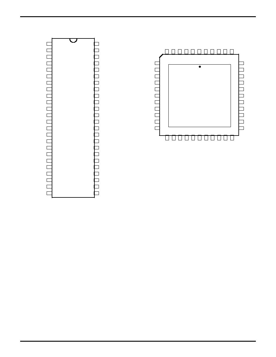
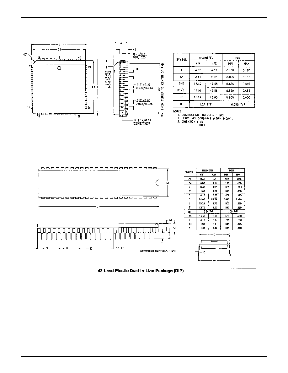
PACKAGE INFORMATION
48-Pin DIP Package Diagram
44-Pin PLCC Package Diagram

40
Z53C80 SCSI
PS97SCC0200
Z
ILOG
ORDERING INFORMATION
Z53C80
48-Pin DIP
44-Pin PLCC
Z53C8003PSC
Z53C8003VSC
Package
P = Plastic DIP
V = Plastic Lead Chip Carrier
Environmental
C = Plastic Standard
Temperature
S = 0
∞
C to +70
∞
C
Speed
3 = 3 MB per second
Example:
Z 53C80 03 V S C
Environmental Flow
Temperature
Package
Speed
Product Number
Zilog Prefix
is a Z53C80, 3 MB/s, PLCC, 0
∞
C to +70
∞
C, Plastic Standard Flow.
Zilog's products are not authorized for use as critical compo-
nents in life support devices or systems unless a specific written
agreement pertaining to such intended use is executed between
the customer and Zilog prior to use. Life support devices or
systems are those which are intended for surgical implantation
into the body, or which sustains life whose failure to perform,
when properly used in accordance with instructions for use
provided in the labeling, can be reasonably expected to result in
significant injury to the user.
Zilog, Inc. 210 East Hacienda Ave.
Campbell, CA 95008-6600
Telephone (408) 370-8000
Telex 910-338-7621
FAX 408 370-8056
Internet: http://www.zilog.com
© 1997 by Zilog, Inc. All rights reserved. No part of this document
may be copied or reproduced in any form or by any means
without the prior written consent of Zilog, Inc. The information in
this document is subject to change without notice. Devices sold
by Zilog, Inc. are covered by warranty and patent indemnification
provisions appearing in Zilog, Inc. Terms and Conditions of Sale
only. Zilog, Inc. makes no warranty, express, statutory, implied or
by description, regarding the information set forth herein or
regarding the freedom of the described devices from intellectual
property infringement. Zilog, Inc. makes no warranty of mer-
chantability or fitness for any purpose. Zilog, Inc. shall not be
responsible for any errors that may appear in this document.
Zilog, Inc. makes no commitment to update or keep current the
information contained in this document.