2-1
Zilog
DS971800500
Z80181
S
MART
A
CCESS
C
ONTROLLER
SAC
TM
PRELIMINARY PRODUCT SPECIFICATION
FEATURES
s
Z80180 Compatible MPU Core with 1 Channel of
Z85C30 SCC, Z80 CTC, Two 8-Bit General-Purpose
Parallel Ports, and Two Chip Select Signals.
s
High Speed Operation (10 MHz)
s
Low Power Consumption in Two Operating Modes:
- (TBD) mA Typ. (Run Mode)
- (TBD) mA Typ. (STOP Mode)
s
Wide Operational Voltage Range (5V
�
10%)
s
TTL/CMOS Compatible
s
Clock Generator
s
One Channel of Z85C30 Serial Communication
Controller (SCC)
Z80181
S
MART
A
CCESS
C
ONTROLLER (SAC
TM
)
s
Z180 Compatible MPU Core Includes:
- Enhanced Z80 CPU Core
- Memory Management Unit (MMU) Enables Access
to 1MB of Memory
- Two Asynchronous Channels
- Two DMA Channels
- Two 16-Bit Timers
- Clocked Serial I/O Port
s
On-Board Z84C30 CTC
s
Two 8-Bit General-Purpose Parallel Ports
s
Memory Configurable RAM and ROM Chip Select Pins
s
100-Pin QFP Package
GENERAL DESCRIPTION
The Z80181 SAC
TM
Smart Access Controller (hereinafter,
referred to as Z181 SAC) is a sophisticated 8-bit CMOS
microprocessor that combines a Z180-compatible MPU
(Z181 MPU), one channel of Z85C30 Serial Communica-
tion Controller (SCC), a Z80 CTC, two 8-bit general-pur-
pose parallel ports, and two chip select signals, into a
single 100-pin Quad Flat Pack (QFP) package (Figures 1
and 2). Created using Zilog's patented Superintegration
TM
methodology of combining proprietary IC cores and cells,
this high-end intelligent peripheral controller is well-suited
for a broad range of intelligent communication control
applications such as terminals, printers, modems, and
slave communication processors for 8-, 16- and 32- bit
MPU based systems.
Information on enhancement/cost reductions of existing
hardware using Z80/Z180 with Z8530/Z85C30 applica-
tions is also included in this product specification.
Notes:
All Signals with a preceding front slash, "/", are active Low, e.g.,
B//W (WORD is active Low); /B/W (BYTE is active Low, only).
Power connections follow conventional descriptions below:
Connection
Circuit
Device
Power
V
CC
V
DD
Ground
GND
V
SS

2-2
Z80181
S
MART
A
CCESS
C
ONTROLLER
SAC
TM
Zilog
DS971800500
GENERAL DESCRIPTION
(Continued)
Z80180
Compatible
Core
Glue
Logic
Address
Decode
Logic
SCC
(1 Channel)
CTC
PIA1
PIA2
Tx Data
Modem/Control
Signals
Bit Programmable
Bi-directional I/O
or I/O Pins of CTC
Bit Programmable
Bi-directional I/O
D7-D0
Control
A19-A0
/ROMCS
/RAMCS
8
8
Z80181 = Z180 + SCC/2 + CTC + PIA
A19-A12
Rx Data
8
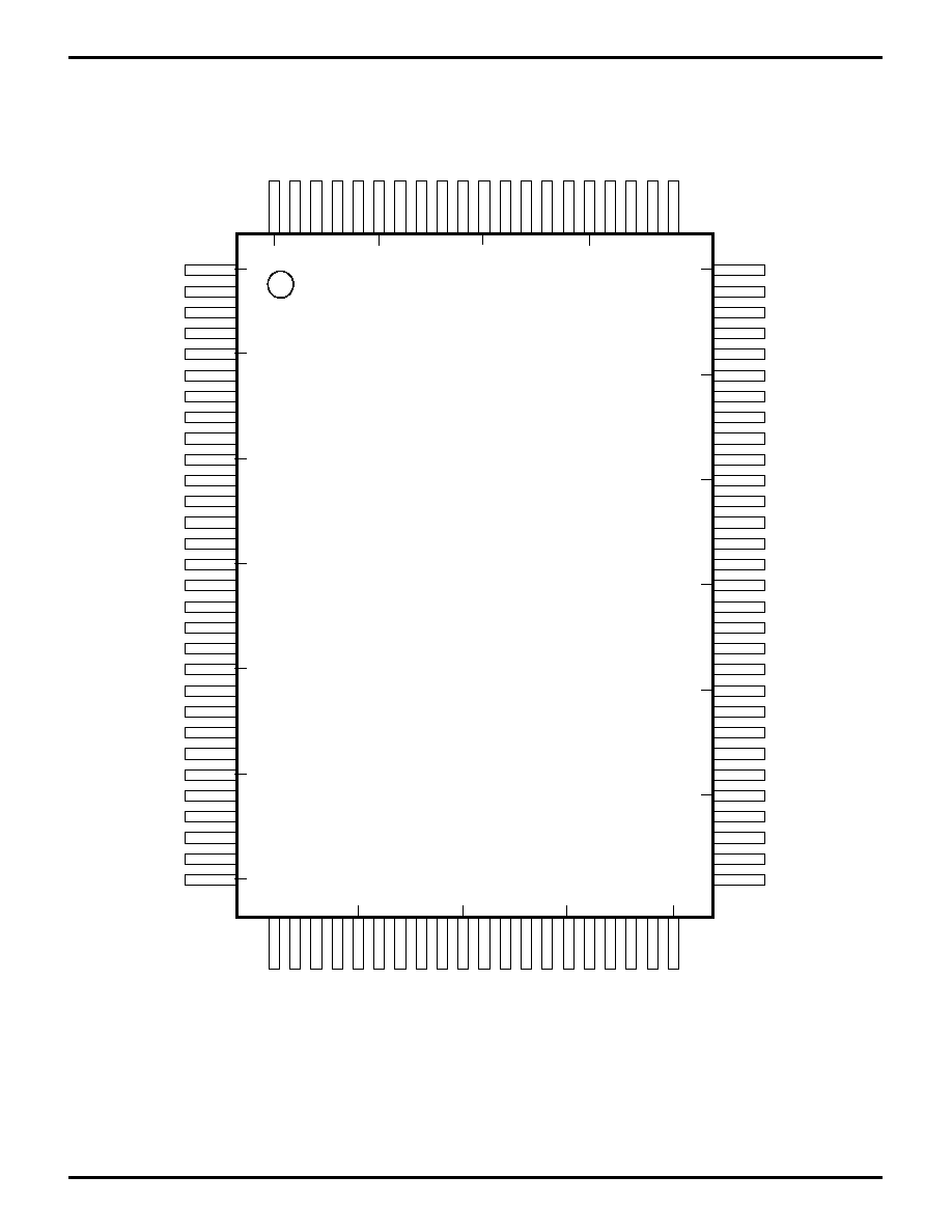
Figure 1. Z80181 Functional Block Diagram
2-3
Zilog
DS971800500
Z80181
S
MART
A
CCESS
C
ONTROLLER
SAC
TM
PIN DESCRIPTION
PIA10
PIA1
1
PIA12
PIA13
P
AI14
PIA15
PIA16
PIA17
+5V
GND
PIA21
PIA22
PIA23
PIA24
PIA25
PIA26
PIA27
/R
TxC
/SYNC
/TEND1
/DREQ1
CKS
RxS//CTS1
TxS
CKA1//TEND0
RxA1
PIA20
/INT
O
/NMI
/RESET
/BUSREQ
/W
AIT
EXT
AL
XT
AL
GND
A17
PHI
/RD
/WR
/M1
E
/MREQ
/IORQ
/RFSH
+5V
/HAL
T
/BUSACK
Z80181
100-Pin QFP
/INT1
/INT2
ST
A0
A1
A2
A3
A15
A4
A5
A6
A7
A8
A9
A10
A11
A12
GND
A13
A14
A16
D0
D1
D2
D3
D4
D5
D6
D7
/RAMCS
TEST
TxA1
CKA0//DREQ0
RxA0
TxA0
/DCD0
/CTS0
/RTS0
A18/TOUT
A19
GND
IEI
/ROMCS
IEO
GND
/DCD
/CTS
/RTS
/DTR//REQ
TxD
/TRxC
RxD
/W//REQ
100
1
95
5
10
15
90
85
80
75
70
65
60
55
50
45
40
35
30
25
20
Figure 2. 100-Pin QFP Pin Configuration

2-4
Z80181
S
MART
A
CCESS
C
ONTROLLER
SAC
TM
Zilog
DS971800500
CPU SIGNALS
Pin Name
Pin Number
Input/Output, Tri-State
Function
A19 - A0
4-17, 19-21,
I/O, Active 1
Address Bus.
A19 - A0 form a 20-bit address bus which
64, 65, 91
specifies I/O and memory addresses to be accessed.
During the refresh period, addresses for refreshing are
output. The address bus enters a high-impedance state
during Reset and external bus acknowledge cycles. The
bus is an input when the external bus master is accessing
the on-chip peripherals. Address line A18 is multiplexed
with the output of PRT Channel 1 (T
OUT
, selected as address
output on Reset).
D0-D7
22-29
I/O, Active 1
8-Bit Bidirectional Data Bus.
When the on-chip CPU is
accessing on-chip peripherals, these lines are outputs
and hold the data to/from the on-chip peripherals.
/RD
89
I/O, Active 0
Read Signal.
CPU read signal for accepting data from
memory or I/O devices. When an external master is ac-
cessing the on-chip peripherals, it is an input signal.
/WR
88
I/O, Active 0
Write Signal.
This signal is active when data to be stored
in a specified memory or peripheral device is on the MPU
data bus. When an external master is accessing the on-
chip peripherals, it is an input signal.
/MREQ
85
I/O, tri-state, Active 0
Memory Request Signal.
When an effective address for
memory access is on the address bus, /MREQ is active.
This signal is analogous to the /ME signal of the Z64180.
/IORQ
84
I/O, tri-state, Active 0
I/O Request Signal.
When addresses for I/O are on the
lower 8 bits (A7-A0) of the address bus in the I/O operation,
"0" is output. In addition, the /IORQ signal is output with the
/M1 signal during the interrupt acknowledge cycle to
inform peripheral devices that the interrupt response vec-
tor is on the data bus. This signal is analogous to the /IOE
signal of the Z64180.
/M1
87
I/O, tri-state, Active 0
Machine Cycle "1".
/MREQ and /M1 are active together
during the operation code fetch cycle. /M1 is output for
every opcode fetch when a two byte opcode is executed.
In the maskable interrupt acknowledge cycle, this signal is
output together with /IORQ. It is also used with
/HALT and ST signal to decode the status of the CPU
Machine cycle. This signal is analogous to the /LIR signal
of the Z64180.
/RFSH
83
Out, tri-state, Active 0
The Refresh Signal.
When the dynamic memory
refresh address is on the low order 8-bits of the address
bus (A7 - A0), /RFSH is active along with the /MREQ signal.
This signal is analogous to the /REF signal of the Z64180.

2-5
Zilog
DS971800500
Z80181
S
MART
A
CCESS
C
ONTROLLER
SAC
TM
Pin Name
Pin Number
Input/Output, Tri-State
Function
/INT0
100
Wired-OR I/O, Active 0
Maskable Interrupt Request 0.
Interrupt is generated by
peripheral devices. This signal is accepted if the interrupt
enable Flip-Flop (IFF) is set to "1". Internally, the SCC and
CTC's interrupt signals are connected to this line, and
require an external pull-up resistor.
/INT1,
1, 2,
In, Active 0
Maskable Interrupt Request 1 and 2.
This signal is
/INT2
generated by external peripheral devices. The CPU hon-
ors these requests at the end of current instruction cycle as
long as the /NMI, /BUSREQ and /INT0 signals are inactive.
The CPU will acknowledge these interrupt requests with an
interrupt acknowledge cycle. Unlike the acknowledgment
for /INT0, during this cycle, neither /M1 or /IORQ will
become active.
/NMI
99
In, Active 0
Non-Maskable Interrupt Request Signal.
This interrupt
request has a higher priority than the maskable interrupt
request and does not rely upon the state of the interrupt
enable Flip-Flop (IFF).
/HALT
81
Out, tri-state, Active 0
Halt Signal.
This signal is asserted after the CPU has
executed either the HALT or SLP instruction, and is waiting
for either non-maskable interrupt maskable interrupt be-
fore operation can resume. It is also used with the /M1 and
ST signals to decode the status of the CPU machine cycle.
/BUSREQ
97
In, Active 0
BUS Request Signal.
This signal is used by external
devices (such as a DMA controller) to request access to
the system bus. This request has higher priority than /NMI
and is always recognized at the end of the current machine
cycle. This signal will stop the CPU from executing further
instructions and place the address bus, data bus, /MREQ,
/IORQ, /RD and /WR signals into the high impedance state.
/BUSREQ is normally wired-OR and a pull-up resistor is
externally connected.
/BUSACK
96
Out, Active 0
Bus Acknowledge Signal.
In response to /BUSREQ sig-
nal, /BUSACK informs a peripheral device that the address
bus, data bus, /MREQ, /IORQ, /RD and /WR signals have
been placed in the high impedance state.
/WAIT
95
Wired-OR I/O, Active 0
Wait Signal.
/WAIT informs the CPU that the specified
memory or peripheral is not ready for a data transfer. As
long as /WAIT signal is active, the MPU is continuously kept
in the wait state. Internally, the /WAIT signal from the SCC
interface logic is connected to this line, and requires an
external pull-up resistor.