
1
P R E L I M I N A R Y
Z80189/Z8L189
G
ENERAL
-P
URPOSE
E
MBEDDED
C
ONTROLLERS
DS971890301
Zilog
P
RELIMINARY
P
RODUCT
S
PECIFICATION
FEATURES
s
Com Port Decode
s
PC DMA Mailbox Registers
s
Host I/O Mailbox
s
Programmable Fixed /ROMCS and
/RAMCS Boundaries
s
100-Pin QFP and VQFP Packages
s
3.3 and 5.0-Volt Operating Ranges
s
0
∞
C to +70
∞
C Temperature Range
Notes:
Enhancements from the Discrete S180 device.
GENERAL DESCRIPTION
Part
CPU
UART
I/O
Speed (MHz)
Z80189
S180*
16550
24
33
Z8L189
S180*
16550
24
20
s
Fully Static Z180
TM
MPU Core*
≠ On-Chip 1 MByte MMU
≠ Two Enhanced UART Channels (up to 512 Kbps)
≠ Two Chain-Linked DMA Channels
≠ x 2 Clock Multiplier
≠ Low-Power Consumption Modes
≠ Two 16-Bit Timer/Counters
≠ Clocked Serial I/O
≠ On-Chip Wait State Generator (WSG)
≠ On-Chip Interrupt Controller
≠
On-Chip Clock Oscillator/Generator
s
16550 Compatible MIMIC Interface
≠ 16 mA MIMIC Output Drive Capability
The Z80189/Z8L189 are cost-effective modem controllers
that address a new generation of data pumps having the
HDLC formatting feature. Data pumps of these types do
not require an HDLC interface; therefore, the Z80189 does
not need the ESCC
TM
. The addition of the PC DMA Mailbox
Registers allow DMA data transfer between the PC memory
and the modem speaker/microphone CODEC. The Z80189
is a smart peripheral controller chip for modem (in particu-
lar V.34 applications), fax, voice messaging, and other
communications applications.
The Z80189/Z8L189 consists of an enhanced Z8S180
microprocessor, a 16550 MIMIC with increased MIMIC
drive capability for direct connection to the IBM PC, XT, AT
bus, and 24 bits of parallel I/O. Current PC modem soft-
ware compatibility can be maintained with the Z80189's
ability to mimic the 16550 UART chip. The Z80180 core is
the intelligent controller between the data pump and
16550 MIMIC interface when used in internal applications.
This intelligent controller performs the data compression
and error correction on outgoing and incoming data.
Z80189/Z8L189
G
ENERAL
-P
URPOSE
E
MBEDDED
C
ONTROLLERS
The integration of COM Port Decode circuitry to the Z80189
allows the MIMIC to be selected for a specific COM Port
Address (PC COM Port Address 1-4). COM Port Decode
circuitry is simplified by allowing the user to select the
MIMIC COM Port addresses through software, in addition
to eliminating the need for external circuitry required for
COM Port Decode logic.
The PC DMA and I/O Mailbox Interface can be used to
provide communication paths between the PC Host and
the Z80189. These new communication paths can be used
for voice, DTAD, or jumperless COM Port selection.
Notes:
All Signals with a preceding front slash, "/", are active Low, e.g.:
B//W (WORD is active Low); /B/W (BYTE is active Low, only).
Power connections follow conventional descriptions below:
Connection
Circuit
Device
Power
V
CC
V
DD
Ground
GND
V
SS

2
P R E L I M I N A R Y
Z80189/Z8L189
G
ENERAL
-P
URPOSE
E
MBEDDED
C
ONTROLLERS
DS971890301
Zilog
GENERAL DESCRIPTION
(Continued)
Figure 1. Z80189 Block Diagram
PC ISA
BUS
Enhanced
S180 MPU
Baud Rate
Generator
16550 MIMIC
Interface
COM Decoder
8-Bit Parallel
Port C
8-Bit Parallel
Port B
8-Bit Parallel
Port A
PC DMA
DMA & I/O
Interface

3
P R E L I M I N A R Y
Z80189/Z8L189
G
ENERAL
-P
URPOSE
E
MBEDDED
C
ONTROLLERS
DS971890301
Zilog
PIN DESCRIPTION
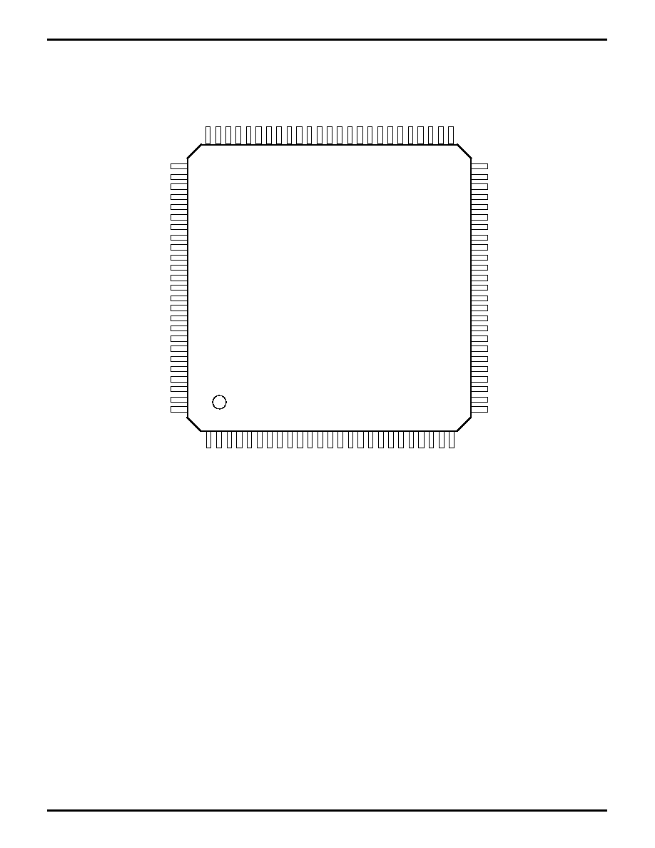
Figure 2. Z80189/Z8L189 100-Lead QFP Pin Identification
HA3//RFSH
HDRQ1//BUSACK
HA4//W
AIT
HA0
/HDDIS/TXA0
/HWR//CTS0
/HRD//DCD0
HINTR2
HAEN
HA6
/NMI
/RESET
/HDACK1//BUSREQ
EXT
AL
XT
AL
PHI
/RD
/WR
/M1
/IOCS2/E
/MRD//MREQ
/IORQ
/HAL
T
VSS
/HCS/HC1
HA2
HA1/RXA0
Z80189/Z8L189
100-Pin QFP
/INT0
/INT1/PC6
/INT2/PC7
ST
A0
A1
A2
A3
A4
A5
A6
A7
A8
A9
A11
A12
VSS
A14
A15
A16
A17
A18
VDD
A19
D0
D1
D3
/RAMCS
VDD
HA7/IEI
/IOCS1/IEO
VSS
HA8
PC4
PC0
PC1
/MWR/PC2
PC3
PC5
HD7/PA7
HD6/PA6
HD5/PA5
HD4/PA4
HD3/PA3
HD2/PA2
HD1/PA1
HD0/PA0
EV2
EV1
/ROMCS
100
1
95
5
10
15
90
85
80
75
70
65
60
55
50
45
40
35
30
25
20
D2
A10
D4
D5
D6
D7
PB0/TXS
PB1//CTS0
PB2//DCD0
PB3/TXA0
PB5/TXA1
PB7/RXS//CTS1
/HDACK0/CKA0//DREQ0
VSS
HA9/CKA1//TEND0
HINTR1/T
OUT
HC2/CKS
HA5//DREQ1
VDD
HDRQ0//R
TS0
PB6/RXA1
PB4/RXA0
A13
4
P R E L I M I N A R Y
Z80189/Z8L189
G
ENERAL
-P
URPOSE
E
MBEDDED
C
ONTROLLERS
DS971890301
Zilog
PIN DESCRIPTION
(Continued)
Figure 3. Z80189/Z8L189 100-Lead VQFP Pin Identification
Z80189/Z8L189
100-Pin VQFP
EV1
/ROMCS
/RAMCS
HDRQ0/RTS0
VDD
HA5//DREQ1
HC2/CKS
HINTR1/TOUT
HA9/CKA1//TEND0
VSS
/HDACK0/CKA0//DREQ0
PB7/RXS//CTS1
PB6/RXA1
PB5/TXA1
PB4/RXA0
PB3/TXA0
PB2//DCD0
PB1//CTS0
PB0/TXS
D7
D6
D5
D4
D3
D2
1
25
/HWR//CTS0
/HRD//DCD0
HINTR2
HAEN
HA6
VDD
HA7/IEI
/IOCS/IEO
VSS
HA8
PC4
PC0
PC1
/MWR/PC2
PC3
PC5
HD7/P
A7
HD6/P
A6
HD5/P
A5
HD4/P
A4
HD3/P
A3
HD2/P
A2
HD1/P
A1
HD0/P
A0
EV2
75
51
5
10
15
20
60
70
55
65
ST
A0
A1
A2
A3
A4
A5
A6
A7
A8
A9
A10
A1
1
A12
VSS
A13
A14
A15
A16
A17
A18
VDD
A19
D0
D1
/HCS/HC1
/HDDIS/TXA0
HA0
HA1/RXA0
HA2
/HALT
HA3//RFSH
/IORQ
/MRD//MREQ
/IOCS2/E
/M1
/WR
/RD
PHI
VSS
XTAL
EXTAL
HA4//WAIT
HDRQ1//BUSACK
/HDACK1//BUSREQ
/RESET
/NMI
/INT0
/INT1/PC6
/INT2/PC7
76
100
80
85
90
95
50
26
30
35
40
45

5
P R E L I M I N A R Y
Z80189/Z8L189
G
ENERAL
-P
URPOSE
E
MBEDDED
C
ONTROLLERS
DS971890301
Zilog
ABSOLUTE MAXIMUM RATINGS
Symbol Description
Min
Max
Units
V
CC
Supply Voltage (*) ≠0.3
+7.0
V
V
IN
Input Voltage
≠0.3
V
CC
+0.3
V
T
OPR
Operating Temp.
0
70
∞
C
T
STG
Storage Temp.
≠55
+150
∞
C
Stresses greater than those listed under Absolute Maxi-
mum Ratings may cause permanent damage to the de-
vice. This is a stress rating only; operation of the device at
any condition above those indicated in the operational
sections of these specifications is not implied. Exposure to
absolute maximum rating conditions for extended periods
may affect device reliability.
STANDARD TEST CONDITIONS
The DC Characteristics and capacitance sections below
apply for the following standard test conditions, unless
otherwise noted. All voltages are referenced to GND (0V).
Positive current flows into the referenced pin (Test Load).
Available operating temperature range is:
S=0
∞
C to 70
∞
C
Voltage Supply Range:
+4.5V
V
CC
+5.5V
+3.0V
V
CC
+3.6V
All AC parameters assume a load capacitance of 50 pF.
Add 10 ns delay for each 50 pF increase in load up to a
maximum of 150 pF for the data bus and 100 pF for
address and control lines. AC timing measurements are
referenced to 1.5 volts (except for clock, which is refer-
enced to the 10% and 90% points). Maximum capacitive
load for PHI is 125 pF.
1.4 V
I
OH
100 pF
OL
I
= 2 mA
= 250
µ
A
Figure 4. Test Load Diagram
Notes:
(*) Voltage on all pins with respect to GND.

6
P R E L I M I N A R Y
Z80189/Z8L189
G
ENERAL
-P
URPOSE
E
MBEDDED
C
ONTROLLERS
DS971890301
Zilog
DC CHARACTERISTICS
Z80189
(V
CC
= 5.0V
±
10% or V
CC
= 3.3v
±
10%, over specified temperature range unless otherwise noted.)
Symbol
Parameter
Min
Typ
Max
Unit
Condition
V
IH1
Input H Voltage
V
CC
≠0.6
V
CC
+0.3
V
RESET, EXTAL, NMI, INT0, INT1, INT2
V
IH2
Input H Voltage
2.0
V
CC
+0.3
V
Except RESET, EXTAL, NMI, INT0, INT1, INT2
V
IL1
Input L Voltage
≠0.3
0.6
V
RESET, EXTAL, NMI, INT0, INT1, INT2
V
IL2
Input L Voltage
≠0.3
0.8
V
Except RESET, EXTAL, NMI, INT0, INT1, INT2
V
OH1
Output H Voltage
V
All outputs
2.4
V
I
OH
= ≠200
µ
A
V
OH2
Output H PHI
V
CC
≠0.6
V
I
OH
= ≠200
µ
A
V
OL1
Output L Voltage
0.40
V
I
OL
= 2.2 mA
All outputs
V
OL2
Output L PHI
0.40
V
I
OL
= 2.2 mA
V
OH
All MIMIC Outputs
2.4
V
I
OH
= 16 mA,**
V
OL
All MIMIC Outputs
0.4
V
I
OL
= 16 mA,**
V
OH
All MIMIC Outputs
2.4
V
I
OH
=8 mA,V
CC
= 3.3 V**
V
OL
All MIMIC Outputs
0.4
V
I
OL
=8 mA,V
CC
= 3.3 V**
I
IL
Input Leakage
10
µ
A
V
IN
= 0 to V
CC
5
Current All Inputs
Except XTAL, EXTAL
I
TL
Tri-State Leakage Current
10
µ
A
V
IN
= 0 to V
CC
5
I
CC
*
Power Dissipation*
18
30
mA
f = 20 MHz, 3.3v
Normal Operation
80
120
mA
f = 33 MHz, 5v
I
CC
*
Power Dissipation*
1.8
3.6
mA
f = 20 MHz, 3.3v
(System STOP Mode)
6
9
mA
f = 33 MHz, 5v
Power Dissipation
15
50
µ
A
(Standby Mode)
Notes:
* V
IH
Min = V
CC
-1.0 V, V
IL
Max = 0.8 V (all output terminals are at no load).
** Total loading current in or out of the Z189 cannot exceed 150 mA from
pins 41 to 70.

7
P R E L I M I N A R Y
Z80189/Z8L189
G
ENERAL
-P
URPOSE
E
MBEDDED
C
ONTROLLERS
DS971890301
Zilog
9
¯
Address
Opcode Fetch Cycle
T1
T2
TW
T3
T1
T2
TW
T3
T1
I/O Write Cycle
I/O Read Cycle
/WAIT
/MREQ
6
1
3
2
4
5
19
20
19
20
7
8
12
11
7
11
29
/IORQ
13
11
13
28
9
/RD
/WR
22
26 and 26a
25
11
10
14
18
/M1
17
ST
Data
IN
Data
OUT
/RESET
15
16
15
16
27
21
23
24
62
63
68
67
62
63
67
68
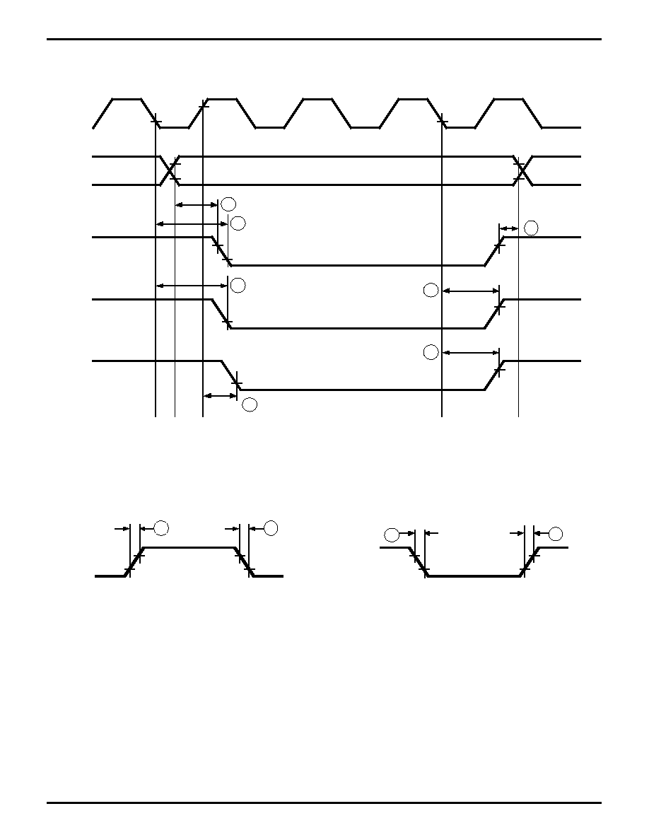
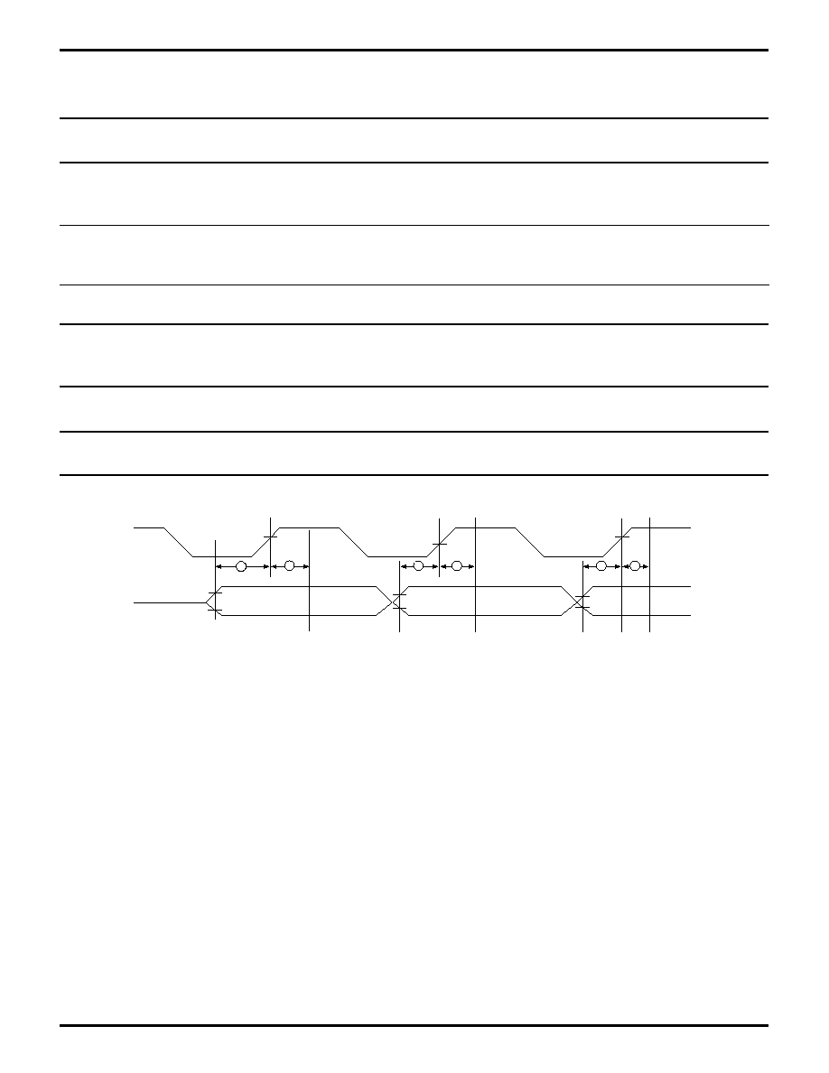
Figure 5. CPU Timing
(Opcode Fetch Cycle, Memory Read/Write Cycle I/O Read/Write Cycle)
TIMING DIAGRAMS

8
P R E L I M I N A R Y
Z80189/Z8L189
G
ENERAL
-P
URPOSE
E
MBEDDED
C
ONTROLLERS
DS971890301
Zilog
Figure 6. CPU Timing
(/INT0 Acknowledge Cycle, Refresh Cycle, BUS RELEASE Mode
HALT Mode, SLEEP Mode, SYSTEM STOP Mode)
TIMING DIAGRAMS
(Continued)
ÿ
32
31
33
30
15
16
39
40
41
42
34
35
35
34
37
36
38
38
43
[3]
/INTI
/NMI
/M1 [1]
/IORQ [1]
/Data IN [1]
/MREQ [2]
/RFSH [2]
/BUSREQ
/BUSACK
Address
Data /MREQ,
/RD, /WR,
/IORQ
/HALT
44
C7
/INTSCC
Notes:
[1] During /INT0 acknowledge cycle
[2] During refresh cycle
[3] Output buffer is off at this point

9
P R E L I M I N A R Y
Z80189/Z8L189
G
ENERAL
-P
URPOSE
E
MBEDDED
C
ONTROLLERS
DS971890301
Zilog
Figure 8. DMA Control Signals
ÿ
45
46
45
45
47
17
48
18
CPU or DMA Read/Write Cycle (Only DMA Write Cycle for /TENDi)
T1
T2
Tw
T3
T1
[3]
[4]
[2]
[1]
/DREQi
(At level
sense)
/DREQi
(At edge
sence)
/TENDi
ST
DMA Control Signals
[
1] tDRQS and tDRQH are specified for the rising edge of clock followed by T3.
[2] tDRQS and tDRQH are specified for the rising edge of clock.
[3] DMA cycle starts.
[4] CPU cycle starts.
Figure 7. CPU Timing
0
Address
/IROQ
T1
T2
TW
T3
T1
13
25
9
/RD
/WR
T2
TW
T3
I/O Read Cycle
I/O Write Cycle
28
29
28
29
22
TIMING DIAGRAMS
(Continued)

10
P R E L I M I N A R Y
Z80189/Z8L189
G
ENERAL
-P
URPOSE
E
MBEDDED
C
ONTROLLERS
DS971890301
Zilog
TIMING DIAGRAMS
(Continued)
ÿ
T1
T2
Tw
Tw
T3
D7-D0
49
50
49
50
49
50
16
15
50
49
ÿ
E
BUS RELEASE Mode
SLEEP Mode
SYSTEM STOP Mode
Figure 9. E Clock Timing
(Memory Read/Write Cycle
I/O Read/Write Cycle)
Figure 10. E Clock Timing

11
P R E L I M I N A R Y
Z80189/Z8L189
G
ENERAL
-P
URPOSE
E
MBEDDED
C
ONTROLLERS
DS971890301
Zilog
ÿ
T2
Tw
T3
T1
T2
E
(Example:
I/O Read -
Opcode
Fetch)
54
49
52
50
53
51
53
49
50
54
E
(I/O Write)
Figure 11. E Clock Timing
(Minimum timing example
of PWEL and PWEH)
Figure 12. Timer Output Timing
ÿ
55
TOUT
Timer Data
Reg = 0000H
TIMING DIAGRAMS
(Continued)

12
P R E L I M I N A R Y
Z80189/Z8L189
G
ENERAL
-P
URPOSE
E
MBEDDED
C
ONTROLLERS
DS971890301
Zilog
TIMING DIAGRAMS
(Continued)
ÿ
T3
T1
T2
TS
TS
T1
T2
32
31
33
43
44
/INTi
/NMI
A18-A0
/MREQ, /M1
/RD
/HALT
SLP Instruction Fetch
Next Opcode Fetch
Figure 13. SLEEP Execution Cycle

13
P R E L I M I N A R Y
Z80189/Z8L189
G
ENERAL
-P
URPOSE
E
MBEDDED
C
ONTROLLERS
DS971890301
Zilog
CSI/O Clock
57
57
59
58
59
58
61
60
60
61
11.5 tcyc
11 tcyc
11 tcyc
11.5 tcyc
16.5 tcyc
16.5 tcyc
56
56
Transmit Data
(Internal Clock)
Transmit Data
(External Clock)
Receive Data
(Internal Clock)
Receive Data
(External Clock)
Figure 14. CSI/O Receive/Transmit Timing
/MREQ
71
/RAMCS
/ROMCS
Figure 15. /ROMCS and /RAMCS Timing
TIMING DIAGRAMS
(Continued)
14
P R E L I M I N A R Y
Z80189/Z8L189
G
ENERAL
-P
URPOSE
E
MBEDDED
C
ONTROLLERS
DS971890301
Zilog
TIMING DIAGRAMS
(Continued)
7
11
T1
T2
TW
T3
T1
Address Valid
0
Address
/MREQ
13
24
8
9
22
/RD
/WR
Figure 16. /MWR and /MRD Timing
EXTAL
VIL1
65
66
VIH1
VIL1
VIH1
Figure 17. External Clock Rise Time and Fall Time
Figure 18. Input Rise and Fall Time
(Except EXTAL, /RESET)
70
69

15
P R E L I M I N A R Y
Z80189/Z8L189
G
ENERAL
-P
URPOSE
E
MBEDDED
C
ONTROLLERS
DS971890301
Zilog
AC CHARACTERISTICS
(V
CC
= 5V
±
10% or V
CC
= 3.3V
±
10%, over specified temperature range unless otherwise noted
33 MHz Characteristics Apply Only to 5V Operation.)
Z8L189-20 MHz
Z80189-33 MHz
No
Sym
Parameter
Min
Max
Min
Max
Unit
Notes
1
tcyc
Clock Cycle Time
50
2000
33
2000
ns
[1]
2
tCHW
Clock H Pulse Width
15
10
ns
[1]
3
tCLW
Clock L Pulse Width
15
10
ns
[1]
4
tcf
Clock Fall Time
10
5
ns
[1]
5
tcr
Clock Rise Time
10
5
ns
[1]
6
tAD
/PHI to Address Valid
15
15
ns
7
tAS
Address Valid to /MREQ, /IRQ
5
5
ns
8
tMED1
/PHI to /MREQ Delay
3
3
ns
[3]
9
tRDD1
/PHI to /RD Delay (IOC=1)
25
15
ns
/ PHI to /RD Delay (IOC=0)
25
15
ns
10
tM1D1
/PHI to /M1 Delay
35
15
ns
11
tAH
Address Hold Time from (MREQ, IOREQ, RD, WR)
5
5
ns
12
tMED2
/PHI to /MREQ Delay
25
15
ns
13
tRDD2
/PHI to /RD Delay
25
15
ns
14
tM1D2
/PHI to /M1 Delay
40
15
ns
15
tDRS
Data Read Setup Time
10
10
ns
[3]
16
tDRH
Data Read Hold Time
0
0
ns
17
tSTD1
/PHI to /ST Delay
30
15
ns
18
tSTD2
/PHI to /ST Delay
30
15
ns
19
tWS
WAIT Setup Time to /PHI
15
10
ns
[2]
20
tWH
WAIT Hold Time from /PHI
10
5
ns
21
tWDZ
/PHI to Data Float Display
35
20
ns
22
tWRD1
/PHI to /WR Delay
25
15
ns
23
tWDD
/PHI to Write Data Delay Time
25
15
ns
24
tWDS
Write Data Setup Time to /WR
10
10
ns
25
tWRD2
/PHI to /WR Delay
25
15
ns
26
tWRP
Write Pulse Width (Memory Write Cycle)
75
45
ns
26a
tWRP
Write Pulse Width (I/O Write Cycle)
130
70
ns
27
tWDH
Write Data Hold Time from /WR
10
5
ns
28
tIOD
/PHI to /IORQ Delay (IOC=1)
25
15
ns
/PHI to /IORQ Delay (IOC=0)
25
15
ns
29
tIOD2
/PHI to /IORQ Delay
25
15
ns
30
tIOD3
/M1 to /IORQ Delay
100
80
ns
31
tINTS
/INT Setup Time to /PHI
20
15
ns
32
tINTH
/INT Hold Time from /PHI
10
10
ns
33
tNMIW
NMI Pulse Width
35
25
ns
34
tBRS
BUSREQ Setup Time to /PHI
10
10
ns
35
tBRH
BUSREQ Hold Time from /PHI
10
10
ns
36
tBAD1
/PHI to /BUSACK Delay
25
15
ns
37
tBAD2
/PHI to /BUSACK Delay
25
15
ns
38
tBZD
/PHI to Bus Floating Delay Time
40
30
ns
39
tMEWH
MREQ Pulse Width (High)
35
25
ns
40
tMEWL
MREQ Pulse Width (Low)
35
25
ns

16
P R E L I M I N A R Y
Z80189/Z8L189
G
ENERAL
-P
URPOSE
E
MBEDDED
C
ONTROLLERS
DS971890301
Zilog
AC CHARACTERISTICS
(Continued)
(V
CC
= 5V
±
10% or V
CC
= 3.3V
±
10%, over specified temperature range unless otherwise noted
33 MHz Characteristics Apply Only to 5V Operation.)
Z8L189-20 MHz
Z80189-33 MHz
No
Sym
Parameter
Min
Max
Min
Max
Unit Notes
41
tRFD1
/PHI to /RFSH Delay
20
15
ns
42
tRFD2
/PHI to /RFSH Delay
20
15
ns
43
tHAD1
/PHI to /HALT Delay
15
15
ns
44
tHAD2
/PHI to /HALT Delay
15
15
ns
45
tDRQS
DREQ Setup Time to /PHI
20
15
ns
46
tDRQH
DREQ Hold Time from /PHI
20
15
ns
47
tTED1
/PHI to /TEND Delay
25
15
ns
48
tTED2
/PHI to /TEND Delay
25
15
ns
49
tED1
/PHI to /E Delay
30
15
ns
50
tED2
/PHI /or to /E Delay
30
15
ns
51
PWEH
E Pulse Width (High)
25
20
ns
52
PWEL
E Pulse Width (Low)
50
40
ns
53
tEr
Enable Rise Time
10
10
ns
54
tEf
Enable Fall Time
10
10
ns
55
tTOD
/PHI to Timer Output Delay
75
50
ns
56
tSTDI
CSI/O Transmit Data Delay (Internal Clock Operation)
75
60
ns
57
tSTDE
CSI/O Transmit Data Delay (External Clock Operation)
7.5 tcyc+75
7.5 tcyc+60
ns
58
tSRSI
CSI/O Receive Data Setup Time (Internal Clock Operation)
1
1
phi cycles
59
tSRHI
CSI/O Receive Data Hold Time (Internal Clock Operation)
1
1
phi cycles
60
tSRSE
CSI/O Receive Data Setup Time (External Clock Operation)
1
1
phi cycles
61
tSRHE
CSI/O Receive Data Hold Time (External Clock Operation)
1
1
phi cycles
62
tRES
RESET Setup Time to /PHI
40
25
ns
63
tREH
RESET Hold Time from /PHI
25
15
ns
64
tOSC
Oscillator Stabilization Time
20
20
ns
65
tEXr
External Clock Rise Time (EXTAL)
10
5
ns
66
tEXf
External Clock Fall Time (EXTAL)
10
5
ns
67
tRr
Reset Rise Time
50
50
ms
[2]
68
tRf
Reset Fall Time
50
50
ms
[2]
69
tIr
Input Rise Time (Except EXTAL, RESET)
50
50
ns
[2]
70
tIf
Input Fall Time (Except EXTAL, RESET)
50
50
ns
[2]
71
tdCS
MREQ Valid to RAMCS and ROMCS Valid Delay
5
5
ns
[3]
Notes:
[1] tcyc = tCHW + tCLW + tcf + tcr.
[2] If the rise and fall times are greater than the specified maximums,
other specifications will not be met.
[3] SL1832 is test screened such that specifications 8, 15, and 71 are
tested to 18 ns (Tmeol + Tors + Trlcs = 18 ns).

17
P R E L I M I N A R Y
Z80189/Z8L189
G
ENERAL
-P
URPOSE
E
MBEDDED
C
ONTROLLERS
DS971890301
Zilog
AC CHARACTERISTICS
(Continued)
Address
5
7
3
Data In
Data Out
A7-A0
/IORQ
/RD
Data
/WR
Data
6
2
2
4
9
8
1
Read/Write External Bus Master Timing
Figure 19. Read/Write External Bus Master Timing

18
P R E L I M I N A R Y
Z80189/Z8L189
G
ENERAL
-P
URPOSE
E
MBEDDED
C
ONTROLLERS
DS971890301
Zilog
AC CHARACTERISTICS
(Continued)
Read/Write External Bus Master Timing
Table 1. External Bus Master Timing
Z8L189-20 MHz
Z80189-33 MHz
No
Sym
Parameter
Min
Max
Min
Max
Unit
Notes
1
TsA(wf)(rf)
Address to WR or RD Fall Time
20
20
ns
2
TsIO(wf)(rf)
IORQ Fall to WR or RD Fall Time
20
20
ns
3
Th
Data Hold Time (from WR Rise)
0
0
ns
4
TdRD(DO)
RD Fall to Data Out Delay
35
35
ns
5
TdRIr(DOz)
RD, IORQ Rise to Data Float Time
0
0
ns
6
TsDI(WRf)
Data In to WR Fall Setup Time
20
20
ns
7
TsA(IORQf)
Address to IORQ Fall Setup Time
35
35
ns
8
TsA(RDf)
Address to RD Fall Setup Time
35
35
ns
9
TsA(WRf)
Address to WR Fall Setup Time
35
35
ns
Table 2. 16550 MIMIC Timing
Z8L189-20 MHz
Z80189-33 MHz
No
Sym
Parameter
Min
Max
Min
Max
Unit
Notes
1
TsAR
Address Setup to HRD Fall Time
30
30
ns
2
TsCSR
Address Setup to CS Fall Time
30
30
ns
3
TsAW
Address Setup to HWR Fall Time
30
30
ns
4
TsCSW
HCS Setup to HWR Fall Time
30
30
ns
5
tAh
Address Hold Time
20
20
ns
6
tCSh
HCS Hold Time
20
20
ns
7
tDs
Data Setup Time
30
30
ns
8
tDh
Data Hold Time
30
30
ns
9
tWc
Write Cycle Delay
2.5
2.5
phi cycles
10
tRvD
Delay from HRD Fall to Data Valid
125
125
ns
11
tHz
HRD Rise to Data Float Delay
100
100
ns
12
tRc
Read Cycle Delay
125
125
ns
13
tRDD
HRD Toggle to Driver Enable/Disable
60
60
ns
14
tSINT
Delay fromwr RBR Reg. to Assert HINTR
2.0
2.0
phi cycles
15
tRINT
Delay from /HRD of RBR to Deassert HINTR
2.0
2.0
phi cycles
16
tHR
Delay from /WR THR to Reset HINTR
2.5
2.5
phi cycles
17
TSTI
Delay from MPU /RD of THR to Assert HINTR
2.0
2.0
phi cycles
18
TIR
Delay from /RD to Reset Interrupt
75
75
ns

19
P R E L I M I N A R Y
Z80189/Z8L189
G
ENERAL
-P
URPOSE
E
MBEDDED
C
ONTROLLERS
DS971890301
Zilog
Valid
HA2, HA1, HA0
/HCS
/HRD
/HWR
1
2
3
4
5
6
Figure 20. PC Host /RD /WR Timing
Table 3. PC Host /RD /WR Timing Table
Z80L189-20 MHz
Z80189-33 MHz
No
Symbol
Parameter
Min
Max
Min
Max
Units
1
TsAR
H Address to/HRD Fall Setup
30
30
ns
2
tsCSR
/HCS to /HRD Fall Setup
30
30
ns
3
tsAW
H Address to /HWR Fall Setup
30
30
ns
4
tsCSW
/HCS to /HRD Fall Setup
30
30
ns
5
tAh
H Address from /HRD /HWR Hold
20
20
ns
6
tCSh
/HCS from /HRD /HWR Hold
20
20
ns
16550 MIMIC TIMING

20
P R E L I M I N A R Y
Z80189/Z8L189
G
ENERAL
-P
URPOSE
E
MBEDDED
C
ONTROLLERS
DS971890301
Zilog
Figure 21. Com Port Decode Mode
PC Host /RD /WR Timing
Table 4. Com Port Decode Mode
PC Host /RD /WR Timing Table
Z8L189-20 MHz
Z80189-33 MHz
No
Symbol
Parameter
Min
Max
Min
Max
Units
1
tsAR
H Address to/HRD Fall Setup
30
30
ns
2
tsCSR
/HCS to /HRD Fall Setup
30
30
ns
3
tsAW
H Address to /HWR Fall Setup
30
30
ns
4
tsCSW
/HCS to /HRD Fall Setup
30
30
ns
5
tAh
H Address from /HRD /HWR Hold
20
20
ns
6
tCSh
/HCS from /HRD /HWR Hold
20
20
ns
Valid
/HA3 - /HA9
HAEN
/HRD
/HWR
1
2
3
4
5
6
16550 MIMIC TIMING
(Continued)

21
P R E L I M I N A R Y
Z80189/Z8L189
G
ENERAL
-P
URPOSE
E
MBEDDED
C
ONTROLLERS
DS971890301
Zilog
Valid
HD7-HD0
/HRD
10
11
12
Figure 23. Data Setup and Hold, Output Delay, Read Cycle
Table 5. Data Setup and Hold, Output Delay, Read Cycle Table
Z8L189-20 MHz
Z80189-33 MHz
No
Sym
Parameter
Min
Max
Min
Max
Units
7
tDs
Data In to /HWR Rise Setup
30
30
ns
8
tDh
Data In from /HWR Rise Hold
30
30
ns
9
tWc
Write Cycle Delay
2.5
2.5
phi cycles
10
tRvd
/HRD Fall to Data Out Valid Delay
125
125
ns
11
THz
/HRD Rise to Data Out Float Delay
100
100
ns
12
tRc
Read Cycle Delay
2.5
2.5
phi cycles
Figure 22. Data Setup and Hold, Output Delay, Write Cycle
Valid
HD7-HD0
/HWR
7
8
9
16550 MIMIC TIMING
(Continued)
22
P R E L I M I N A R Y
Z80189/Z8L189
G
ENERAL
-P
URPOSE
E
MBEDDED
C
ONTROLLERS
DS971890301
Zilog
16550 MIMIC TIMING
(Continued)
/HRD
/HDDIS
13
Figure 24. Driver Enable Timing
Table 6. Driver Enable Timing Table
Z8L189-20 MHz
Z80189-33 MHz
No
Sym
Parameter
Min
Max
Min
Max
Units
13
tRDD
/HRD to Driver
Enable/Disable
60
60
ns
Figure 25. Interrupt Timing RCVR FIFO
14
14
15
15
/WR (MPU)
RBR
HINTR
(Trigger
Level)
HINTR
(Line
Status
RDR
/HRD LSR
/HRD RBR
23
P R E L I M I N A R Y
Z80189/Z8L189
G
ENERAL
-P
URPOSE
E
MBEDDED
C
ONTROLLERS
DS971890301
Zilog
16550 MIMIC TIMING
(Continued)
Table 7. Interrupt Timing RCVR FIFO Table
Z8L189-20 MHz
Z80189-33 MHz
Units
No
Sym
Parameter
Min
Max
Min
Max
14
tSINT
Delay from Stop to Set
2
2
phi cycles
Interrupt
15
tRINT
Delay from /HRD
(RD RBR or RD LSR)
2
2
phi cycles
to Reset Interrupt
/RD (MPU)
TxFIFO
HINTR
THRE
/WR (Host)
THR
/RD (Host)
11R
17
16
18
Figure 26. Interrupt Timing Transmitter FIFO
24
P R E L I M I N A R Y
Z80189/Z8L189
G
ENERAL
-P
URPOSE
E
MBEDDED
C
ONTROLLERS
DS971890301
Zilog
16550 MIMIC TIMING
(Continued)
Table 8. Interrupt Timing Transmitter FIFO Table
Z8L189-20 MHz
Z80189-33 MHz
No
Sym
Parameter
Min
Max
Min
Max
Units
16
tHR
Delay from /WR
2.5
2.5
phi cycles
(WR THR) to Reset
Interrupt
17
TSTI
Delay from Stop to
2
2
phi cycles
Interrupt (THRE)
18
TIR
Delay from /RD to
2.5
2.5
phi cycles
Reset Interrupt
Table 9. I/O Port Timing Table
Z8L189-20 MHz
Z80189-33 MHz
No
Sym
Parameter
Min
Max
Min
Max
Units
1
TsPIA(WR)
Data Setup Time to (Port) WR Fall
20
20
ns
2
TdWR(PIA)
Data Valid Delay from WR Rise
60
60
ns
Port (Output)
Port Output Data 1 (Out)
Port Output Data 2 (Out)
/WR
Port
1
2
1
2
1
2
Figure 27. I/O Port Timing Diagram

25
P R E L I M I N A R Y
Z80189/Z8L189
G
ENERAL
-P
URPOSE
E
MBEDDED
C
ONTROLLERS
DS971890301
Zilog
PC DMA TIMING
Table 10. PC DMA Mailbox Timing
PD DMA Write: Memory-Read, I/O Write DMA Bus Cycle
Z8L189-20 MHz
Z80189-33 MHz
No
Sym
Parameter
Min
Max
Min
Max
Units
1
tACKWh
/HDACK Active Hold
144
144
ns
/HWR Inactive
2
tWRs
/HDACK Active to
301
301
ns
/HWR Active
3
tWR
/HWR Active to
454
454
ns
Inactive
4
tvWR
Data Valid to /HWR
133
133
ns
Inactive
5
tDWRh
Write Data Valid Hold
25
25
ns
from /HWR Inactive
Table 11. PC DMA Mailbox Timing
PD DMA Read: I/O-Read, Memory-Write DMA Bus Cycle
Z8L189-20 MHz
Z80189-33 MHz
No
Sym
Parameter
Min
Max
Min
Max
Units
1
tACKRh
/HDACK Active Hold
89
89
ns
/HRD Inactive
2
tRDs
/HDACK Active to
62
62
ns
/HRD Active
3
tRD
/HRD Active to
749
749
ns
Inactive
4
tvRD
Data Valid from /HRD
215
215
ns
Active
5
tDRDh
Read Data Valid Hold
0
0
ns
from /HRD Inactive
6
tDZ
Data Float from /HRD
50
50
ns
Inactive

26
P R E L I M I N A R Y
Z80189/Z8L189
G
ENERAL
-P
URPOSE
E
MBEDDED
C
ONTROLLERS
DS971890301
Zilog
PC DMA TIMING DIAGRAMS
Figure 28. PC DMA Write: Memory-Read, I/O Write
DMA Bus Cycle on PC AT Bus
Figure 29. PC DMA Read: I/O-Read, Memory-Write
DMA Bus Cycle on PC AT Bus
PC Clock
Internal
HDRQR
HDRQ
/AEN
/HDACK
/HWR
HD [0:7]
Valid
3
4
5
1
2
(1)
(1) The HDRQ will not fall inactive until it ses the
falling edge of /HWR during the /HDACK cycle.
PC Clock
Internal
HDRQR
HDRQ
/AEN
/HDACK
/HRD
HD [0:7]
Valid
3
6
5
2
4
(1)
1
(1) The HDRQ will not fall inactive until it sees the
falling edge of /HRD during the /HDACK cycle
.

27
P R E L I M I N A R Y
Z80189/Z8L189
G
ENERAL
-P
URPOSE
E
MBEDDED
C
ONTROLLERS
DS971890301
Zilog
PIN DESCRIPTION
CPU Signals
A19-A0.
Address Bus (Input/Output, active High, tri-state).
A0-A19 form a 20-bit address bus. The Address Bus
provides the address for memory data bus exchanges, up
to 1 Mbyte, and I/O data bus exchanges, up to 64K. The
address bus enters a high impedance state during reset
and external bus acknowledge cycles, as well as during
SLEEP and HALT states. This bus is an input when the
external bus master is accessing the on-chip peripherals.
D7-D0.
Data Bus (Bidirectional, active High, tri-state). D0-
D7 constitute an 8-bit bidirectional data bus, used for the
transfer of information to and from I/O and memory de-
vices. The data bus enters the high impedance state
during reset and external bus acknowledge cycles, as well
as during SLEEP and HALT states.
/RD.
Read (Input/Output, active Low, tri-state). /RD indi-
cates that the CPU wants to read data from memory or an
I/O device. The addressed I/O or memory device should
use this signal to gate data onto the CPU data bus.
/WR.
Write (Output, active Low, tri-state). /WR indicates
that the CPU data bus holds valid data to be stored at the
addressed I/O or memory location.
/IORQ.
I/O Request (Input/Output, active Low, tri-state).
/IORQ indicates that the address bus contains a valid I/O
address for an I/O read or I/O write operation. /IORQ is also
generated, along with /M1, during the acknowledgment of
the /INT0 input signal to indicate that an interrupt response
vector can be placed onto the data bus.
/M1.
Machine Cycle 1 (Input/Output, active Low). Together
with /MREQ, /M1 indicates that the current cycle is the
opcode fetch cycle of an instruction execution. Together
with /IORQ, /M1 indicates that the current cycle is for an
interrupt acknowledge. It is also used with the /HALT and
ST signal to decode status of the CPU machine cycle.
/MREQ.
Memory Request (Input/Output, active Low, tri-
state). /MREQ indicates that the address bus holds a valid
address for a memory read or memory write operation.
/WAIT.
(Input, active Low). /WAIT indicates to the MPU that
the addressed memory or I/O devices are not ready for a
data transfer. This input is used to induce additional clock
cycles into the current machine cycle. The /WAIT input is
sampled on the falling edge of t2 (and subsequent wait
states). If the input is sampled low, then additional wait
states are inserted until the /WAIT input is sampled high, at
which time execution will continue.
/HALT.
Halt/Sleep Status (Output, active Low). This output
is asserted after the CPU has executed either the HALT or
SLP instruction, and is waiting for either non-maskable or
maskable interrupt before operation can resume. It is also
used with the /M1 and ST signals to decode status of the
CPU machine cycle. On exit of Halt/Sleep, the first instruc-
tion fetch is delayed 16 clock cycles after the /HALT pin
goes high.
/BUSACK.
Bus Acknowledge (Output, active Low
tri-state). /BUSACK indicates to the requesting device, the
MPU address and data bus, and some control signals,
have entered their high-impedance state.
/BUSREQ.
Bus Request (Input, active Low). This input is
used by external devices (such as DMA controllers) to
request access to the system bus. This request has a
higher priority than /NMI and is always recognized at the
end of the current machine cycle. This signal will stop the
CPU from executing further instructions and places the
address and data buses, and other control signals, into the
high impedance state.
/NMI.
Non-maskable interrupt (Input, negative edge trig-
gered). /NMI has a higher priority than /INT and is always
recognized at the end of an instruction, regardless of the
state of the interrupt enable flip-flops. This signal forces
CPU execution to continue at location 0066H.
/INT0.
Maskable Interrupt Request 0 (Input, active Low).
This signal is generated by external I/O devices. The CPU
will honor this request at the end of the current instruction
cycle as long as the /NMI and /BUSREQ signals are
inactive. The CPU acknowledges this interrupt request
with an interrupt acknowledge cycle. During this cycle,
both the /M1 and /IORQ signals will become active.
/INT1, /INT2.
Maskable Interrupt Requests 1 and 2 (inputs,
active Low). This signal is generated by external I/O
devices. The CPU will honor these requests at the end of
the current instruction cycle as long as the /NMI, /BUSREQ,
and /INT0 signals are inactive. The CPU will acknowledge
these interrupt requests with an interrupt acknowledge
cycle. Unlike the acknowledgment for /INT0, during this
cycle neither the /M1 or /IORQ signals will become active.
These pins may be programmed to provide active low
level, rising or falling edge interrupts. The level of the
external /INT1 and /INT2 pins may be read through bits
PC6 and PC7 of parallel port C.

28
P R E L I M I N A R Y
Z80189/Z8L189
G
ENERAL
-P
URPOSE
E
MBEDDED
C
ONTROLLERS
DS971890301
Zilog
PIN DESCRIPTION
(Continued)
/RFSH.
Refresh (Output, active Low, tri-state). Together
with /MREQ,/RFSH indicates that the current CPU machine
cycle and the contents of the address bus should be used
for refresh of dynamic memories. The low order 8 bits of the
address bus (A7-A0) contain the refresh address.
/MRD.
Memory Read (Output, active Low, tri-state). /MRD
is active when both the internal /MREQ and /RD signals are
active.
/MWR.
Memory write (output, active Low, tri-state). /MWR
is active when both the internal /MREQ and /WR signals are
active.
Z180
TM
MPU UART and SIO Signals
CKA0, CKA1.
Asynchronous Clock 0 and 1 (Bidirectional,
active High). When in output mode, these pins are
the transmit and receive clock outputs from the ASCI
baud rate generators. When in input mode, these pins
serve as the external clock inputs for the ASCI baud rate
generators.
CKS.
Serial Clock (Bidirectional, active High). This line is
the clock for the CSIO channel.
/DCD0.
Data Carrier Detect 0 (Input, active Low). This is a
programmable modem control signal for ASCI channel 0.
/RTS0.
Request to Send 0 (Output, active Low, tri-state).
This is a programmable modem control signal for ASCI
channel 0.
/CTS0/CTS1.
Clear to Send 0 (Input, active Low). This line
is a modem control signal for the ASCI channel 0 and 1.
TXA0.
Transmit Data 0 (Output, active High). This signal is
the transmitted data from the ASCI channel 0.
TXS.
Clocked Serial Transmit Data (Output, active High).
This line is the transmitted data from the CSIO channel.
RXA0.
Receive Data 0 (Input, active High). This signal is
the receive data to ASCI channel 0.
RXS.
Clocked Serial Receive Data (Input, active High).
This line is the receiver data for the CSIO channel.
RXA1.
Received Data ASCI Channel 1.
TXA1.
Transmitted Data ASCI Channel 1.
Z180
TM
MPU DMA Signals
/TEND0.
Transfer End 0 (outputs, active Low). This output
is asserted active during the last write cycle of a DMA
operation. It is used to indicate the end of the block
transfer.
/DREQ0, /DREQ1.
DMA request 0 and 1 (Input, active
Low). /DREQ is used to request a DMA transfer from one
of the on-chip DMA channels. The DMA channels monitor
these inputs to determine when an external device is ready
for a read or write operation. These inputs can be pro-
grammed to be either level or edge sensed.
Z180
TM
MPU Timer Signals
T
OUT
.
Timer Out (Output, active High). T
OUT
is the pulse
output from PRT channel 1. This line is multiplexed with
HINTR1 of the 16550 MIMIC.
16550 MIMIC Interface Signals
HD7-HD0.
Host Data Bus (Input/Output, tri-state). In
Z80189, the host data bus is used to communicate be-
tween the 16550 MIMIC interface and the PC/XT/AT. It is
multiplexed with the PA7-PA0 of parallel port A.
/HDDIS.
Host Driver Disable (Output, active Low). In
Z80189, this signal goes low whenever the PC/XT/AT is
reading data from the 16550 MIMIC interface. The /HDDIS
pin should also go active low on each PC DMA read cycle.
HA2-HA0.
Host Address (Input). In Z80189, these pins are
the address inputs to the 16550 MIMIC interface. This
address determines which register the PC/XT/AT accesses.
HA9-HA3, HAEN.
Host COM Port Decode Address (In-
put). In Z80189, these pins are multiplexed when COM
Port Decode is enabled (default). These pins are used to
provide internal MIMIC Enable when HA9-HA3 match the
programmed MIMIC address field. HAEN is also used to
access the PC DMA Mailbox registers.
/HCS.
Host Chip Select (Input, active Low). In Z80189, this
input is used by the PC/XT/AT to select the 16550 MIMIC
interface for an access. The /HCS input is disabled when
using the internal COM Port Decoder. When setting the
/HCS Force bit in the CDR register, the /HCS output is
asserted when HA3-HA9 is within the boundaries pro-
grammed by bits 3-4 of the CDR register and /HRD or
/HWR is asserted. /HCS is NOT asserted for PC DMA
Mailbox accesses.

29
P R E L I M I N A R Y
Z80189/Z8L189
G
ENERAL
-P
URPOSE
E
MBEDDED
C
ONTROLLERS
DS971890301
Zilog
/HWR.
Host Write (Input, active Low). In Z80189, this input
is used by the PC/XT/AT to signal the 16550 MIMIC
interface that a write operation is taking place.
/HRD.
Host Read (Input, active Low). In Z80189, this input
is used by the PC/XT/AT to signal the 16550 MIMIC
interface that a read operation is taking place.
HINTR1, HINTR2.
Host Interrupt (Output, active High tri-
state). In Z80189, this output is used by the 16550 MIMIC
interface to signal the PC/XT/AT that an interrupt is pend-
ing. In Z80189 COM Port Decode mode, the MIMIC inter-
rupt request can be routed to either HINTR1 or 2 depend-
ing on the COM Port Decode selected. The deselected
HINTR line will be forced to tri-state, while the selected
HINTR will follow what is programmed in the MIMIC Master
Control Register.
HC1, HC2.
Host COM Select Pin 1&2 (Input). HC1 and HC2
are general-purpose inputs that can be used for COM Port
selection. The status of these pins are read by use of the
CDR register. The status of these pins can be used by
firmware to select the appropriate COM Port address
decode range.
PC DMA Mailbox Signals
/HDACK0, /HDACK1.
Host DMA Acknowledge (Input,
active Low). This input signal indicates to the Z80189 that
the PC DMA controller has acknowledged the request and
will begin data transfer. /HDACK0 is multiplexed with
/CKA0 and /DREQ0. /HDACK1 is multiplexed with
/BUSREQ.
HDRQ0, HDRQ1.
Host DMA Request (output, active high,
tri-state). This output requests to the PC DMA controller
that the Z80189 is ready for a DMA data transfer. HDRQ is
multiplexed with /RTS0. HDRQ1 is multiplexed with
/BUSACK.
Parallel Ports
PA7-PA0.
Parallel Port A (Input/Output). These lines can
be configured as inputs or outputs on a bit-by-bit basis
when the Z80189 is operated in mode 0.
PB7-PB0.
Parallel Port B (Input/Output). These lines can
be configured as inputs or outputs on a bit-by-bit basis
when the port function is selected in the System
Configuration register.
PC7-PC0.
Parallel Port C (Input/Output). These lines can
be configured as inputs or outputs on a bit by bit basis for
bits PC5-PC0. Bits PC7 and PC6 are input only and read
the level of the external /INT2 and /INT1 pins. When /INT2
and/or /INT1 are in edge capture mode writing a `1' to the
respective PC7, PC6 bit clears the interrupt capture latch.
Writing a `0' has no effect.
Emulation Signals
EV1, EV2.
Emulation Select (Input). These two pins
determine the emulation mode the Z180 MPU is in. They
are as follows:
EV2 EV1
Mode 0 0
0
Normal mode, on-chip Z180 bus
master.
Mode 1 0
1
Emulation Adapter Mode
Mode 2 1
0
Emulator Probe Mode
Mode 3 1
1
Reserved
System Control Signals
ST.
Status (Output, active High). This signal is used with
the M1 and /HALT output to decode the status of the CPU
machine cycle.
/RESET.
Reset Signal (Input, Active Low). /RESET signal
is used for initializing the MPU and other devices in the
system. It must be kept in the active state for a period of at
least 6 system clock cycles.
IEI.
Interrupt Enable Signal (Input, active High). IEI is used
with the IEO to form a priority daisy chain when there is
more than one interrupt driven peripheral.
IE0.
Interrupt Enable Output Signal (Output, active High).
In the daisy-chain interrupt control, IEO controls the interrupt
of external peripherals. IEO is active when IEI is "1" and the
CPU is not servicing an interrupt from the on-chip
peripherals. This pin is multiplexed with /IOCS1.
/IOCS1.
I/O Chip Select 1
(output, active Low)
is an
auxiliary chip select that decodes A7, A6, /IORQ, /M1 and
effectively decodes the address space XX80 to XXBF for
I/O transactions. A15 through A8 are not decoded so that
the chip select is active in all pages of I/O address space.
The /IOCS1 function is the default on power on or reset
condition and is changed by programming bit 2 in the
Interrupt Edge/Pin Mux Register.

30
P R E L I M I N A R Y
Z80189/Z8L189
G
ENERAL
-P
URPOSE
E
MBEDDED
C
ONTROLLERS
DS971890301
Zilog
System Control Signals
(Continued)
/IOCS2.
I/O Chip Select 2 (output, active Low) This pin is
a secondary peripheral I/O chip select. This pin is active for
I/O accesses between XXC0H to XXC7H or XXC8H to
XXCFH (programmable by bit 1 of the IOBRG register).
/RAMCS.
RAM Chip Select (Output, active Low). Signal
used to access RAM based upon the address and the
RAMLBR and RAMUBR registers.
/ROMCS.
ROM Chip Select (Output, active Low). Signal
used to access ROM based upon the address and the
ROMBR register.
XTAL.
Crystal (Output, active High). Crystal oscillator
connection. This pin should be left open if an external clock
is used instead of a crystal. The oscillator input is not a TTL
level (reference DC characteristics).
EXTAL.
External Clock/Crystal (Input, active High). Crystal
oscillator connections. An external clock can be input to
the Z80189 on this pin when a crystal is not used. This input
is Schmitt-triggered.
PHI.
System Clock (Output, active High). The output is
used as a reference clock of the MPU and the external
system.
V
CC
.
Power Supply. +5 Volts
V
SS
.
Power Supply. 0 Volts
PIN MULTIPLEXING
To allow for COM Port decode and omission of ESCC core,
Pin Multiplexing is changed with respect to the Z182.
ESCC CH.A pins will be replaced by COM Decode and
ASCI CH.A pins as follows:
RxDA
HA6
/TRxCA
HAEN
TxDA
HINTR2
DCDB
/HRD//DCD0
/CTSB
/HWR//CTS0
Note that ASCI channel 0 functions can be found in two
places. These pins are ORed with ASCI channel 0 func-
tions that are multiplexed with Port B (pins 35-39 QFP).
/DCD0, /CTS0, RXA0 inputs will come from 78, 79, 81
(respectively) when Port B (0-4) is enabled. When MIMIC
is disabled, /HDDIS pin doubles as TXA0 output. Note that
/RTS0 has also been changed to pin 50.
When COM decode bit is set (enabled during reset) the
following pins become multiplexed as follows.
/RFSH
HA3
/WAIT
HA4
/DREQ1
HA5
/HA6
HA6
IEI
HA7
/HA8
HA8
CKA1/TEND0
HA9
/HAEN
HAEN
These pins are selected such that they are all high-z inputs
at power up to prevent any problems with connecting
address lines directly to PC bus. Although, the COM
decode multiplexing is enabled on power-up, the COM
address decoding is disabled.

31
P R E L I M I N A R Y
Z80189/Z8L189
G
ENERAL
-P
URPOSE
E
MBEDDED
C
ONTROLLERS
DS971890301
Zilog
Table 12. Z80189 Pin-Out
Multiplexed Pin Descriptions Primary, Secondary Pin Functions
PIN #
PIN #
DEFAULT
SECONDARY
VQFP
QFP
FUNCTION
FUNCTION
CONTROL
1
4
ST
2
5
A0
3
6
A1
4
7
A2
5
8
A3
6
9
A4
7
10
A5
8
11
A6
9
12
A7
10
13
A8
11
14
A9
12
15
A10
13
16
A11
14
17
A12
15
18
V
SS
16
19
A13
17
20
A14
18
21
A15
19
22
A16
20
23
A17
21
24
A18
22
25
V
DD
23
26
A19
24
27
D0
25
28
D1
26
29
D2
27
30
D3
28
31
D4
29
32
D5
30
33
D6

32
P R E L I M I N A R Y
Z80189/Z8L189
G
ENERAL
-P
URPOSE
E
MBEDDED
C
ONTROLLERS
DS971890301
Zilog
PIN MULTIPLEXING
(Continued)
Table 12. Z80189 Pin-Out (Continued)
Multiplexed Pin Descriptions Primary, Secondary Pin Functions
PIN #
PIN #
DEFAULT
SECONDARY
VQFP
QFP
FUNCTION
FUNCTION
CONTROL
31
34
D7
32
35
PB0
TXS
System Config Reg bit 5
33
36
PB1
/CTS0
System Config Reg bit 5
34
37
PB2
/DCD0
System Config Reg bit 5
35
38
PB3
TXA0
System Config Reg bit 5
36
39
PB4
RXA0
System Config Reg bit 5
37
40
PB5
TXA1
System Config Reg bit 6
38
41
PB6
RXA1
System Config Reg bit 6
39
42
PB7
RXS//CTS1
System Config Reg bit 6
40
43
/HDACK0
CKA0//DREQ0
Host DMA Enable Reg bit 3
41
44
V
SS
42
45
HA9
CKA1//TENDO
COM Decode Reg bit 0
43
46
HINTR1
T
OUT
System Config Reg bit 2
44
47
HC2
CKS
COM Decode Reg bit 0
45
48
HA5
/DREQ1
(4)
46
49
V
DD
47
50
HDRQ0
/RTSO
(6) Host DMA Enable Reg bit 3
48
51
/RAMCS
49
52
/ROMCS
50
53
EV1
51
54
EV2
52
55
HD0
PA0
Sys Config Reg bit 1
53
56
HD1
PA1
Sys Config Reg bit 1
54
57
HD2
PA2
Sys Config Reg bit 1
55
58
HD3
PA3
Sys Config Reg bit 1
56
59
HD4
PA4
Sys Config Reg bit 1
57
60
HD5
PA5
Sys Config Reg bit 1
58
61
HD6
PA6
Sys Config Reg bit 1
59
62
HD7
PA7
Sys Config Reg bit 1

33
P R E L I M I N A R Y
Z80189/Z8L189
G
ENERAL
-P
URPOSE
E
MBEDDED
C
ONTROLLERS
DS971890301
Zilog
Z80189 MPU FUNCTIONAL DESCRIPTION
The Z80189 includes a Zilog Z8S180 MPU (Static Z80180
MPU). This allows software code compatibility with exist-
ing Z80/Z180
software code. The following is an overview
of the major functional units of the Z80189.
Architecture
The Z80189 combines a high performance CPU core with
a variety of system and I/O resources useful in a broad
range of applications. The CPU core consists of four
functional blocks:
s
Clock Generator
s
Bus State Controller (Dynamic Memory Refresh)
s
Memory Management Unit (MMU)
s
Central Processing Unit (CPU).
The integrated I/O resources make up the remaining
functional blocks:
s
Direct Memory Access (DMA control--two channels)
s
Asynchronous Serial Communications Controller
(ASCI, two channels)
s
Programmable Reload Timers (PRT, two channels)
s
Clocked Serial I/O
s
16550 Compatible MIMIC Interface
s
COM Port Decoder
s
PC DMA Mailbox Registers
s
Host I/O Mailbox Registers
Clock Generator.
This logic generates the system clock
from either an external crystal or clock input. The external
clock is divided by two, or one if programmed, and is
provided to both internal and external devices.
In addition, there is also a clock multiplier feature which
doubles the internal clock frequency from that of the
external clock input.
Bus State Controller.
This logic performs all of the status
and bus control activity associated with both the CPU and
some on-chip peripherals. This includes wait state timing,
reset cycles, DRAM refresh, and DMA bus exchanges.
Interrupt Controller.
This logic monitors and prioritizes
the variety of internal and external interrupts and traps to
provide the correct responses from the CPU. To maintain
compatibility with the Z80 CPU, three different interrupt
modes are supported.
Memory Management Unit.
The MMU allows the user to
"map" the memory used by the CPU (logically only 64
Kbytes) into the 1 Mbyte addressing range supported by
the Z80189. The organization of the MMU object code
maintains compatibility with the Z80 CPU while offering
access to an extended memory space. This is accom-
plished by using an effective "common area-banked area"
scheme.
Central Processing Unit.
The CPU is microcoded to
provide a core that is object-code compatible with the Z80
CPU. It also provides a superset of the Z80 instruction set,
including 8-bit multiply. This core has been modified to
allow many of the instructions to execute in fewer clock
cycles.

34
P R E L I M I N A R Y
Z80189/Z8L189
G
ENERAL
-P
URPOSE
E
MBEDDED
C
ONTROLLERS
DS971890301
Zilog
Table 12. Z80189 Pin-Out (Continued)
Multiplexed Pin Descriptions Primary, Secondary Pin Functions
PIN #
PIN #
DEFAULT
SECONDARY
VQFP
QFP
FUNCTION
FUNCTION
CONTROL
60
63
PC5
61
64
PC3
62
65
PC2
/MWR
Int Edge/Pin Reg bit 3
63
66
PC1
64
67
PC0
65
68
PC4
66
69
HA8
67
70
V
SS
68
71
/IOCS1
IEO
Int Edge/Pin reg bit 2
69
72
HA7
IEI
(1) COM Decode reg bit 0
70
73
V
DD
71
74
HA6
72
75
HAEN
73
76
HINTR2
74
77
/HRD
/DCD0
(2)
75
78
/HWR
/CTS0
(2)
76
79
/HDDIS
TXA0
Sys Conf reg bit 1
77
80
HA0
78
81
HA1
RXA0
(2)
79
82
HA2
80
83
/HCS
HC1
(3)
81
84
/HALT
82
85
HA3
/RFSH
COM Decode reg bit 0
83
86
/IORQ
84
87
/MREQ
/MRD
Int Edge/Pin Reg bit 3
85
88
/IOCS2
E
I/O brg reg bit 2
86
89
/M1
87
90
/WR
88
91
/RD
89
92
PHI
90
93
V
SS
91
94
XTAL
92
95
EXTAL
93
96
HA4
/WAIT
(5) COM Decode reg bit 0
94
97
HDRQ1
/BUSACK
(6) Host DMA Enable Reg bit 2
95
98
/HDACK1
/BUSREQ
(5) Host DMA Enable Reg bit 2
96
99
/RESET
97
100
/NMI
98
1
/INT0
99
2
/INT1
PC6
100
3
/INT2
PC7
All inputs feature an auto latch that assures that an uncon-
nected input is seen as a logic high or logic low by both the
Z189 or any measurement device connected to the inputs.
The auto latch will latch onto the previous state of input pin.
Notes:
1. IEI pulled high internally when default function is active
2. Pins also act as ASCI inputs only when Port B is enabled
3. MIMIC access is disabled until the system configuration register is
written. /HCS can be forced to output the result of COM Port Decoder.
4. Pin simultaneously acts as input for both default and secondary
functions.
5. /WAIT is pulled high internally when default function is active.
6. Upon power-up or reset, this pin is tri-state.
35
P R E L I M I N A R Y
Z80189/Z8L189
G
ENERAL
-P
URPOSE
E
MBEDDED
C
ONTROLLERS
DS971890301
Zilog
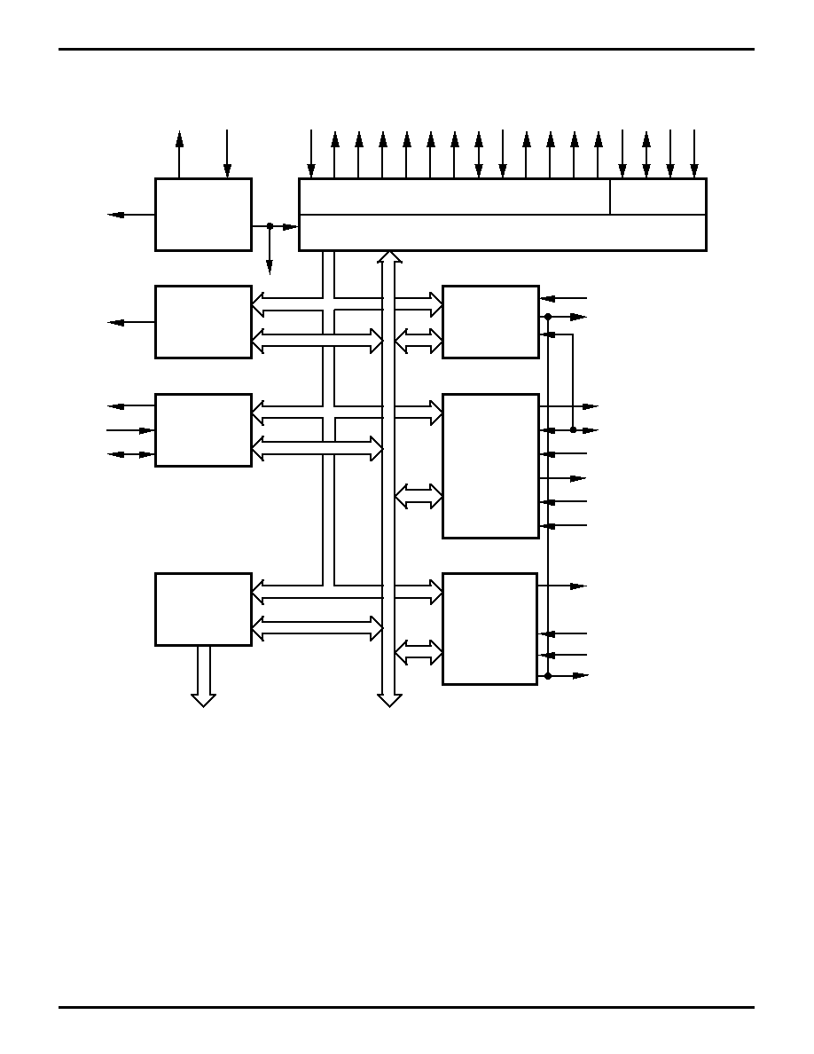
Figure 30. Z189 MPU Block Diagram
Timing &
Clock
Generator
Bus State Control
Interrupt
CPU
DMACs
(2)
16-Bit
Programmable
Reload Timers
(2)
Clocked
Serial I/O
Port
Asynchronous
SCI
(Channel 0)
Asynchronous
SCI
(Channel 1)
MMU
Data Bus (8-Bit)
Address Bus (16-Bit)
/DREQ1
/TEND0
TxA0
CKA0/ /DREQ0
RxA0
/RTS0
/CTS0
/DCD0
TxA1
RxA1
ÿ
TOUT
TxS
RxS
CKS
XT
AL
EXT
AL
/RESET
/RD
/WR
/M1
/MREQ
/IORQ
/HAL
T
/W
AIT
/BUSREQ
/BUSACK
/RFSH
ST
E
/NMI
/INT0
/INT1
/INT2
A19-A0
D7-D0
/CTS1
/CKA1
36
P R E L I M I N A R Y
Z80189/Z8L189
G
ENERAL
-P
URPOSE
E
MBEDDED
C
ONTROLLERS
DS971890301
Zilog
Z80189 MPU FUNCTIONAL DESCRIPTION
(Continued)
DMA Controller
DMA Controller.
The DMA controller provides high-speed
transfers between memory and I/O devices. Transfer op-
erations supported are memory-to-memory, memory to or
from I/O, and I/O-to-I/O. Transfer modes supported are
request, burst, and cycle steal. DMA transfers can access
the full 1 Mbyte addressing range with a block length up to
64 Kbytes, and can cross over the 64 Kbytes boundaries.
Asynchronous Serial Communications
Interface (ASCI)
The ASCI logic provides two individual full-duplex UARTs.
Each channel includes a programmable baud rate gen-
erator. The ASCI channels can also support a multiproces-
sor communications format. For ASCI0, up to three modem
control signals and one clock signal can be pinned out,
while ASCI1 has a data-only interface and 1 clock signal.
The receiver includes a 4-byte FIFO, plus a shift register as
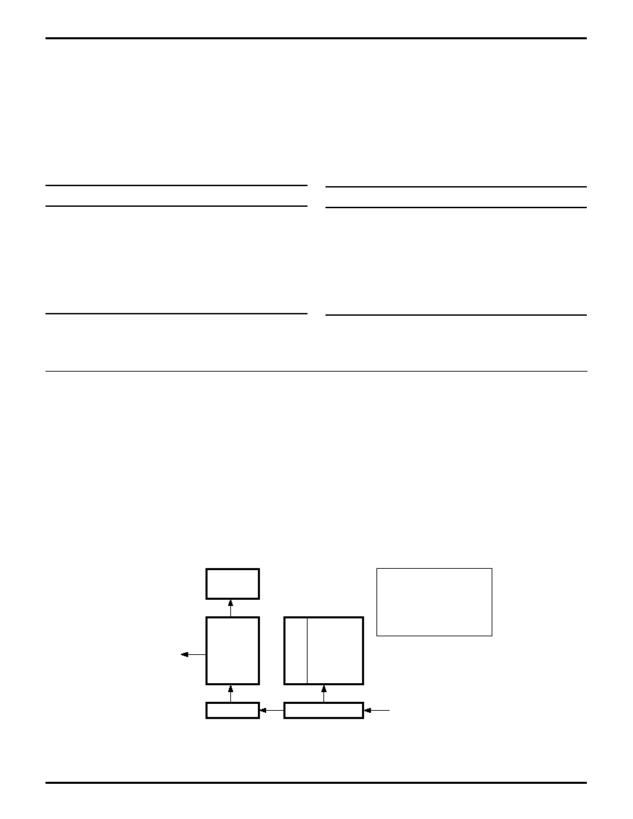
shown in Figure 31.
Reset DCD (ASCI0 with Auto Enables) and
I/O Stop Mode Conditions
During Reset and in I/O Stop state, and for ASCI0 if /DCD0
is auto-enabled and is High, an ASCI is forced to the
following conditions:
s
FIFO Empty
s
All Error Bits Cleared (including those in the FIFO)
s
Receive Enable Cleared (cntla bit 6 = 0)
s
Transmit Enable Cleared (cntla bit 5 = 0).
If DCD is not auto-enabled, the /DCD pin has no effect on
the FIFOs or enable bits.
Figure 31. ASCI Receiver
Error
Latches
4x4 Bit
Error
FIFO
P F O B
E E R K
MP
Bit
4-Byte
Data FIFO
Error
Shift Register
RXA
Overrun
Error
Notes:
PE = Parity Error
FE = Framing Error
OR = Overrun
BK = Break
MP = Multiprocessor Bit
SM1-0
SAR18-16
Source
11
000
ext (CKA0/DREQ)
11
001
ASCI0 Rx
11
010
ASCI1 Rx
11
011
ext (/DREQ1)
11
100
*
11
101
*
11
110
*
11
111
*
DM1-0
DAR18-16
Destination
11
000
ext (CKA0//DREQ0)
11
001
ASCI0 Tx
11
010
ASCI1 Tx
11
011
ext (/DREQ1)
11
100
*
11
101
*
11
110
*
11
111
*
* Reserved do not use.
Table 13. SAR18-16 and DAR18-16 I/O Device Encoding

37
P R E L I M I N A R Y
Z80189/Z8L189
G
ENERAL
-P
URPOSE
E
MBEDDED
C
ONTROLLERS
DS971890301
Zilog
FIFO and Receiver Operation
The 4-byte Receive FIFO is used to buffer incoming data
to reduce the incidence of overrun errors. When the RE bit
is set in the CNTLA register, the RXA pin is monitored for
a Low transition. One-half bit time after the Low transition
of the RXA pin, the ASCI samples RXA again. If it has gone
back to High, the ASCI ignores the previous Low transition
and resumes looking for a new one, but if RXA is still Low,
it considers this a start bit and proceeds to clock in the data
based upon the internal baud rate generator or the exter-
nal CKA pin. The number of data bits, parity, multiproces-
sor and stop bits are selected by the MOD2, MOD1, MOD0
and MP bits in the CNTLA and CNTLB registers. After the
data has been received, the appropriate MP, parity and
one stop bit are checked. Data and any errors are clocked
into the FIFOs during the stop bit. Interrupts, Receive Data
Register Full Flag, and DMA requests will also go active
during this time.
Error Condition Handling
When the receiver places a data character in the Receive
FIFO, it also places any associated error conditions in the
error FIFO. The outputs of the error FIFO go to the set inputs
of the software-accessible error latches. Writing a 0 to
CNTLA EFR is the only way to clear these latches. In other
words, when an error bit reaches the top of the FIFO, it sets
an error latch. If the FIFO has more data and the software
reads the next byte out of the FIFO, the error latch remains
set, until the software writes a 0 to the EFR bit. The error bits
are cumulative, so if additional errors are in the FIFO, they
will set any upset error latches as they reach the top.
Overrun Error
An overrun occurs if the receive FIFO is full when the
receiver has just assembled a byte in the shift register and
is ready to transfer it to the FIFO. If this occurs, the overrun
error bit associated with the previous byte in the FIFO is
set. The latest data byte is not transferred from the shift
register to the FIFO in this case, and is lost. Once an
overrun occurs, the receiver does not place any further
data in the FIFO, until the "last good byte received" has
come to the top of the FIFO so that the Overrun latch is set,
and software then clears the Overrun latch. Assembly of
bytes continues in the shift register, but this data is ignored
until the byte with the overrun error reaches the top of the
FIFO and is cleared with a write of 0 to the EFR bit.
Break Detect
A Break is defined as a framing error with the data equal to
all zeros. When a break occurs, the all-zero byte with its
associated error bits are transferred to the FIFO, if it is not
full. If the FIFO is full, an overrun is generated, but the
break, framing error and data, are not transferred to the
FIFO. Any time a break is detected, the receiver will not
receive any more data until the RXA pin returns to a High
state. If the channel is set in multiprocessor mode and the
MPE bit of the CNTLA register is set to 1, then breaks,
errors and data will be ignored unless the MP bit in the
transmission is a 1. Note: The two conditions listed above
could cause a break condition to be missed if the FIFO is
full and the break occurs, or if the MP bit in the transmission
is not a 1 with the conditions specified above.
Parity and Framing Errors
Parity and Framing Errors do not affect subsequent re-
ceiver operation.

38
P R E L I M I N A R Y
Z80189/Z8L189
G
ENERAL
-P
URPOSE
E
MBEDDED
C
ONTROLLERS
DS971890301
Zilog
Z80189 MPU FUNCTIONAL DESCRIPTION
(Continued)
Baud Rate Generator
The Baud Rate Generator (BRG) has two modes. The first
is the same as in the Z80180. The second is a 16-bit down
counter that divides the processor clock by the value in a
16-bit time constant register, and is identical to the ESCC
BRG. This allows a common baud rate of up to 512 Kbps
to be selected. The BRG can also be disabled in favor of
an external clock on the CKA pin.
The Receiver and Transmitter will subsequently divide the
output of the BRG (or the signal from the CKA pin) by 1, 16
or 64, under the control of the DR bit in the CNTLB register,
and the X1 bit in the ASCI Extension Control Register. To
compute baud rate, use the following formulas.
If ss2,1,0 = 111, baud rate = f
CKA
/ Clock mode
else if BRG mode baud rate = f
PHI
/ (2 * (TC+2) * Clock
mode)
else baud rate = f
PHI
/ ((10 + 20*PS) * 2^ss * Clock mode)
Where:
BRG mode is bit 3 of the ASEXT register
PS is bit 5 of the CNTLB register
TC is the 16-bit value in the ASCI Time Constant registers
The TC value for a given baud rate is:
TC = (f
PHI
/ (2 * baud rate * Clock mode)) - 2
Clock mode depends on bit 4 in ASEXT and bit 3 in CNTLB:
X1
DR
Clock Mode
0
0
=
16
0
1
=
64
1
0
=
1
1
1
=
Reserved, do not use.
2^ss depends on the three LS bits of the CNTLB register:
ss2
ss1
ss0
2^ss
0
0
0
=
1
0
0
1
=
2
0
1
0
=
4
0
1
1
=
8
1
0
0
=
16
1
0
1
=
32
1
1
0
=
64
1
1
1
=
External Clock from CKA0
(see above).
The requirement of having very close to the 50% duty cycle
when the CKA pin is used as an input, has been removed
on the 189. Minimum High and Low times on CKA0 are
typical of most CMOS devices.
RDRF is set, and if enabled an Rx Interrupt or DMA
Request is generated, when the receiver transfers a char-
acter from the Rx Shift Register to the Rx FIFO. The FIFO
merely provides margin against overruns. When there's
more than one character in the FIFO, and software or a
DMA channel reads a character, RDRF either remains set
or is cleared and then immediately set again. Similarly, if a
receive interrupt service routine doesn't read all the char-
acters in the RxFIFO, RDRF and the interrupt request
remain asserted.
The Rx DMA request is disabled when any of the error flags
PE or FE or OVRN are set, so that software can identify with
which character the problem is associated.
Programmable Reload Timer (PRT)
This logic consists of two separate channels, each con-
taining a 16-bit counter (timer) and count reload register.
The time base for the counters is derived from the system
clock (divided by 20) before reaching the counter. PRT
channel 1 provides an optional output to allow for wave-
form generation.
The T
OUT
output of PRT1 is available on a multiplexed pin.
Clocked Serial I/O (CSIO)
The CSI0 channel provides a half-duplex serial transmitter
and receiver. This channel can be used for simple high-
speed data connection to another microprocessor or
microcomputer.

39
P R E L I M I N A R Y
Z80189/Z8L189
G
ENERAL
-P
URPOSE
E
MBEDDED
C
ONTROLLERS
DS971890301
Zilog
/M1
If the M1E bit of the operation Mode Control Register is set
to 1, the RETI cycle occurs only once. The /M1 output is
asserted LOW during the opcode fetch cycle, the /INT0
acknowledge cycle, and the first machine cycle of the /NMI
acknowledge. When M1E bit is rest to 0, the /M1 output is
normally inactive an asserted LOW only during the refetch
of the RETI instruction sequence and during /INTO
acknowledge cycle.
Z8S180 POWER-DOWN MODES
The following is a detailed description of the enhance-
ments to the Z8S180 from the standard Z80180 in the areas
of STANDBY, IDLE, and STANDBY-QUICK RECOVERY
modes.
Add-On Features
There are five different power-down modes. SLEEP and
SYSTEM STOP are inherited from the Z80180. In SLEEP
Table 14. Power Down Modes
Power-Down
CPU
On-Chip
Recovery
Recovery Time
Modes
Core
I/O
OSC.
CLKOUT
Source
(Minimum)
SLEEP
Stop
Running
Running
Running
RESET, Interrupts
1.5 Clock
I/O STOP
Running
Stop
Running
Running
By Programming
-
SYSTEM STOP
Stop
Stop
Running
Running
RESET, Interrupts
1.5 Clock
IDLE
Stop
Stop
Running
Stop
RESET, Interrupts, BUSREQ
8 +1.5 Clock
STANDBY
Stop
Stop
Stop
Stop
RESET, Interrupts, BUSREQ
2
17
+1.5 Clock (Normal Recovery)
2
6
+1.5 Clock (Quick Recovery)
mode, the CPU is in a stopped state while the on-chip
I/Os are still operating. In I/O STOP mode, the on-chip I/Os
are in a stopped state while leaving the CPU running. In
SYSTEM STOP mode, both the CPU and the on-chip I/Os
are in the stopped state to reduce current consumption.
The Z8S180 has added two additional power-down modes,
STANDBY and IDLE, to reduce current consumption even
further. The differences in these power-down modes are
summarized in Table 14.
Notes:
IDLE and STANDBY modes are only offered in the Z8S180. Note that the
minimum recovery time can be achieved if INTERRUPT is used as the
Recovery Source.

40
P R E L I M I N A R Y
Z80189/Z8L189
G
ENERAL
-P
URPOSE
E
MBEDDED
C
ONTROLLERS
DS971890301
Zilog
STANDBY Mode
The Z8S180 has been designed to save power. Two low-
power programmable power-down modes have been
added; STANDBY mode and IDLE mode. The
STANDBY/IDLE mode is selected by multiplexing D6 and
D3 of the CPU Control Register (CCR, I/O Address = 1FH).
To enter STANDBY mode:
1.
Set D6 and D3 to 1 and 0, respectively.
2.
Set the I/O STOP bit (D5 of ICR,
I/O Address = 3FH) to 1.
3.
Execute the SLEEP instruction.
When the part is in STANDBY mode, it behaves similar to
the SYSTEM STOP mode which currently exists on the
Z80180, except that the STANDBY mode stops the clock
oscillator, internal clocks and reduces the power con-
sumption to a minimum.
Since the clock oscillator has been stopped, a restart of the
oscillator requires a period of time for stabilization. An 18-
bit counter has been added in the Z8S180 to allow for
oscillator stabilization. When the part receives an external
IRQ or BUSREQ during STANDBY mode, the oscillator is
restarted and the timer counts down 2
17
counts before
acknowledgment is sent to the interrupt source.
The recovery source needs to remain asserted for duration
of the 2
17
count, otherwise standby will be resumed.
The following is a description of how the part exits STANDBY
for different interrupts and modes of operation.
STANDBY Mode Exit with /RESET
The /RESET input needs to be asserted for a duration long
enough for the crystal oscillator to stabilize and then exit
from the STANDBY mode. When /RESET is de-asserted, it
goes through the normal reset timing to start instruction
execution at address (logical and physical) 0000H.
The clocking is resumed within the Z8S180 and at the
system clock output after /RESET is asserted when the
crystal oscillator is restarted, but not yet stabilized.
STANDBY Mode Exit with BUS REQUEST
Optionally, if the BREXT bit (D5 of CPU Control Register) is
set to 1, the Z8S180 exits STANDBY mode when the
/BUSREQ input is asserted; the crystal oscillator is then
restarted. An internal counter automatically provides time
for the oscillator to stabilize, before the internal clocking
and the system clock output of the Z8S180 are resumed.
The Z8S180 relinquishes the system bus after the clocking
is resumed by:
- Tri-State the address outputs A19 through A0.
- Tri-State the bus control outputs /MREQ, /IORQ,
/RD and /WR.
- Asserting /BUSACK.
The Z8S180 regains the system bus when /BUSREQ is
deactivated. The address outputs and the bus control
outputs are then driven High; the STANDBY mode is
exited.
If the BREXT bit of the CPU Control Register (CCR) is
cleared, asserting the /BUSREQ would not cause the
Z8S180 to exit STANDBY mode.
If STANDBY mode is exited due to a reset or an external
interrupt, the Z8S180 remains relinquished from the sys-
tem bus as long as /BUSREQ is active.

41
P R E L I M I N A R Y
Z80189/Z8L189
G
ENERAL
-P
URPOSE
E
MBEDDED
C
ONTROLLERS
DS971890301
Zilog
STANDBY Mode Exit with External Interrupts
STANDBY mode can be exited by asserting input /NMI.
The STANDBY mode may also exit by asserting /INT0,
/INT1 or /INT2, depending on the conditions specified in
the following paragraphs.
/INT0 wake-up requires assertion throughout duration of
clock stabilization time (2
17
clocks).
If exit conditions are met, the internal counter provides time
for the crystal oscillator to stabilize, before the internal
clocking and the system clock output within the Z8S180
are resumed.
1.
Exit with Non-Maskable Interrupts
If /NMI is asserted, the CPU begins a normal NMI interrupt
acknowledge sequence after clocking resumes.
2.
Exit with External Maskable Interrupts
If an External Maskable Interrupt input is asserted, the CPU
responds according to the status of the Global Interrupt
Enable Flag IEF1 (determined by the ITE1 bit) and the
settings of the corresponding interrupt enable bit in the
Interrupt/Trap Control Register (ITC: I/O Address = 34H):
a.
If an interrupt source is disabled in the ITC, asserting
the corresponding interrupt input would not cause the
Z8S180 to exit STANDBY mode. This is true regardless
of the state of the Global Interrupt Enable Flag IEF1.
b.
If the Global Interrupt Flag IEF1 is set to 1, and if an
interrupt source is enabled in the ITC, asserting the
corresponding interrupt input causes the Z8S180 to
exit STANDBY mode. The CPU performs an interrupt
acknowledge sequence appropriate to the input be-
ing asserted when clocking is resumed if:
- The interrupt input follows the normal interrupt
daisy chain protocol.
- The interrupt source is active until the acknowledge
cycle is completed.
c.
If the Global Interrupt Flag IEF1 is disabled, i.e., reset
to 0, and if an interrupt source is enabled in the ITC,
asserting the corresponding interrupt input will still
cause the Z8S180 to exit STANDBY mode. The CPU
will proceed to fetch and execute instructions that
follow the SLEEP instruction when clocking is re-
sumed.
If the External Maskable Interrupt input is not active when
clocking resumes, the Z8S180 will not exit STANDBY
mode. If the Non-Maskable Interrupt (/NMI) is not active
when clocking resumes, the Z8S180 still exits the STANDBY
mode even if the interrupt sources go away before the
timer times out, because /NMI is edge-triggered. The
condition is latched internally once /NMI is asserted Low.
IDLE Mode
IDLE mode is another power-down mode offered by the
Z8S180. To enter IDLE mode:
1.
Set D6 and D3 to 0 and 1, respectively.
2.
Set the I/O STOP bit (D5 of ICR,
I/O Address = 3FH) to 1.
3.
Execute the SLEEP instruction.
When the part is in IDLE mode, the clock oscillator is kept
oscillating, but the clock to the rest of the internal circuit,
including the CLKOUT, is stopped completely. IDLE mode
is exited in a similar way as STANDBY mode, i.e., RESET,
BUS REQUEST or EXTERNAL INTERRUPTS, except that
the 2
17
bit wake-up timer is bypassed; all control signals are
asserted eight clock cycles after the exit conditions are
gathered.
STANDBY-QUICK RECOVERY Mode
STANDBY-QUICK RECOVERY mode is an option offered
in STANDBY mode to reduce the clock recovery time in
STANDBY mode from 2
17
clock cycles (6.5 ms at 20 MHz)
to 2
6
clock cycles (3.2
µ
s at 20 MHz).
This feature can only
be used when providing an oscillator as clock source.
To enter STANDBY-QUICK RECOVERY mode:
1.
Set D6 and D3 to 1 and 1, respectively.
2.
Set the I/O STOP bit (D5 of ICR,
I/O Address = 3FH) to 1.
3.
Execute the SLEEP instruction.
When the part is in STANDBY-QUICK RECOVERY mode,
the operation is identical to STANDBY mode except when
exit conditions are gathered, i.e., RESET, BUS REQUEST
or EXTERNAL INTERRUPTS; the clock and other control
signals are recovered sooner than the STANDBY mode.
Note:
If STANDBY-QUICK RECOVERY is enabled, the
user must make sure stable oscillation is obtained within
64 clock cycles.

42
P R E L I M I N A R Y
Z80189/Z8L189
G
ENERAL
-P
URPOSE
E
MBEDDED
C
ONTROLLERS
DS971890301
Zilog
Z8S180 MPU REGISTER MAP
Notes:
Registers listed in
boldface type
represent new registers
added to the Z8S180.
All register addresses not listed are Reserved.
Register Name
I/O Addr/Access
ASCI Control Register A Ch 0
%0000/40/80 R/W
ASCI Control Register A Ch 1
%0001/41/81 R/W
ASCI Control Register B Ch 0
%0002/42/82 R/W
ASCI Control Register B Ch 1
%0003/43/83 R/W
ASCI Status Register Ch 0
%0004/44/84 R/W
ASCI Status Register Ch 1
%0005/45/85 R/W
ASCI TX Data Register Ch 0
%0006/46/86 R/W
ASCI TX Data Register Ch 1
%0007/47/87 R/W
ASCI RX Data Register Ch 0
%0008/48/88 R/W
ASCI RX Data Register Ch 1
%0009/49/89 R/W
CSIO Control Register
%000A/4A/8A R/W
CSIO Transmit/Receive Data Reg.
%000B/4B/8B R/W
Timer Data Register Ch OL
%000C/4C/8C R/W
Timer Data Register Ch OH
%000D/4D/8D R/W
Reload Register Ch OL
%000E/4E/8E R/W
Reload Register Ch OH
%000F/4F/8F R/W
Timer Control Register
%0010/50/90
ASCI0 Extension Control Reg.
%0012/52/92 R/W
ASCI1 Extension Control Reg.
%0013/53/93 R/W
Timer Data Register Ch 1L
%0014/54/94 R/W
Timer Data Register Ch 1H
%0015/55/95 R/W
Timer Reload Register Ch 1L
%0016/56/96 R/W
Timer Reload Register Ch 1H
%0017/57/97 R/W
Free Running Counter
%0018/58/98 R/W
ASCI0 Time Constant Low
%001A/5A/9A R/W
ASCI0 Time Constant High
%001B/5B/9B R/W
ASCI1 Time Constant Low
%001C/5C/9C R/W
ASCI1 Time Constant High
%001D/5D/9D RW
Clock Multiplier Register
%001E/5E/9E RW
Register Name
I/O Addr/Access
CPU Control Register
%001F/5F/9F R/W
DMA Source Addr Register Ch OL
%0020/60/A0 R/W
DMA Source Addr Register Ch OH
%0021/61/A1 R/W
DMA Source Addr Register Ch OB
%0022/62/A2 R/W
DMA Dest Addr Register Ch OL
%0023/63/A3 R/W
DMA Dest Addr Register Ch OH
%0024/64/A4 R/W
DMA Dest Addr Register Ch OB
%0025/65/A5 R/W
DMA Byte Count Register Ch OL
%0026/66/A6 R/W
DMA Byte Count Register Ch OH
%0027/67/A7 R/W
DMA Memory Addr Register Ch 1L
%0028/68/A8 R/W
DMA Memory Addr Register Ch 1H
%0029/69/A9 R/W
DMA Memory Addr Register Ch 1B
%002A/6A/AA R/W
DMA I/O Addr Register Ch 1L
%002B/6B/AB R/W
DMA I/O Addr Register Ch 1H
%002C/6C/AC R/W
DMA I/O Addr Register Ch 1B
%002D/6D/AD R/W
DMA Byte Count Register Ch 1L
%002E/6E/AE R/W
DMA Byte Count Register Ch 1H
%002F/6F/AF R/W
DMA Status Register
%0030/70/B0 R/W
DMA Mode Register
%0031/71/B1 R/W
DMA/WAIT Control Register
%0032/72/B2 R/W
IL Register
%0033/73/B3 R/W
INT/TRAP Control Register
%0034/74/B4 R/W
Refresh Control Register
%0036/76/B6 R/W
MMU Common Base Register
%0038/78/B8 R/W
MMU Bank Base Register
%0039/79/B9 R/W
MMU Common/Bank Area Register
%003A/7A/BA R/W
Operation Mode Control Register
%003E/7E/BE R/W
I/O Control Register
%003F/7F/BF R/W
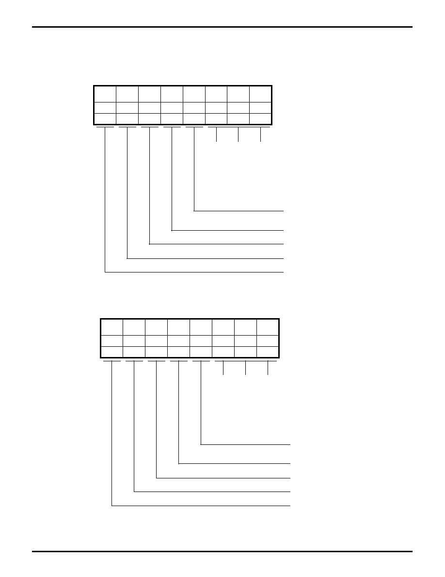
43
P R E L I M I N A R Y
Z80189/Z8L189
G
ENERAL
-P
URPOSE
E
MBEDDED
C
ONTROLLERS
DS971890301
Zilog
Z8S180 MPU REGISTERS
ASCI CHANNELS CONTROL REGISTERS
Figure 33. ASCI Control Register A (Ch. 1)
MPE
RE
TE
/RTS0
MPBR/
EFR
MOD2 MOD1 MOD0
0
R/W
0
R/W
0
R/W
1
R/W
x
R/W
0
R/W
0
R/W
0
R/W
Bit
Upon RESET
R/W
CNTLA0
MODE Selection
Addr 00H
Read - Multiprocessor Bit Receive
Write - Error Flag Reset
Request To Send
Transmit Enable
Receive Enable
Multiprocessor Enable
0 0 0 Start + 7-Bit Data + 1 Stop
0 0 1 Start + 7-Bit Data + 2 Stop
0 1 0 Start + 7-Bit Data + Parity + 1 Stop
0 1 1 Start + 7-Bit Data + Parity + 2 Stop
1 0 0 Start + 8-Bit Data + 1 Stop
1 0 1 Start + 8-Bit Data + 2 Stop
1 1 0 Start + 8-Bit Data + Parity + 1 Stop
1 1 1 Start + 8-Bit Data + Parity + 2 Stop
Figure 32. ASCI Control Register A (Ch. 0)
MPE
RE
TE
CKA1D MPBR/
EFR
MOD2 MOD1 MOD0
0
R/W
0
R/W
0
R/W
1
R/W
x
R/W
0
R/W
0
R/W
0
R/W
Bit
Upon RESET
R/W
CNTLA1
MODE Selection
Addr 01H
Read - Multiprocessor Bit Receive
Write - Error Flag Reset
CKA1 Disable
Transmit Enable
Receive Enable
Multiprocessor Enable
0 0 0 Start + 7-Bit Data + 1 Stop
0 0 1 Start + 7-Bit Data + 2 Stop
0 1 0 Start + 7-Bit Data + Parity + 1 Stop
0 1 1 Start + 7-Bit Data + Parity + 2 Stop
1 0 0 Start + 8-Bit Data + 1 Stop
1 0 1 Start + 8-Bit Data + 2 Stop
1 1 0 Start + 8-Bit Data + Parity + 1 Stop
1 1 1 Start + 8-Bit Data + Parity + 2 Stop
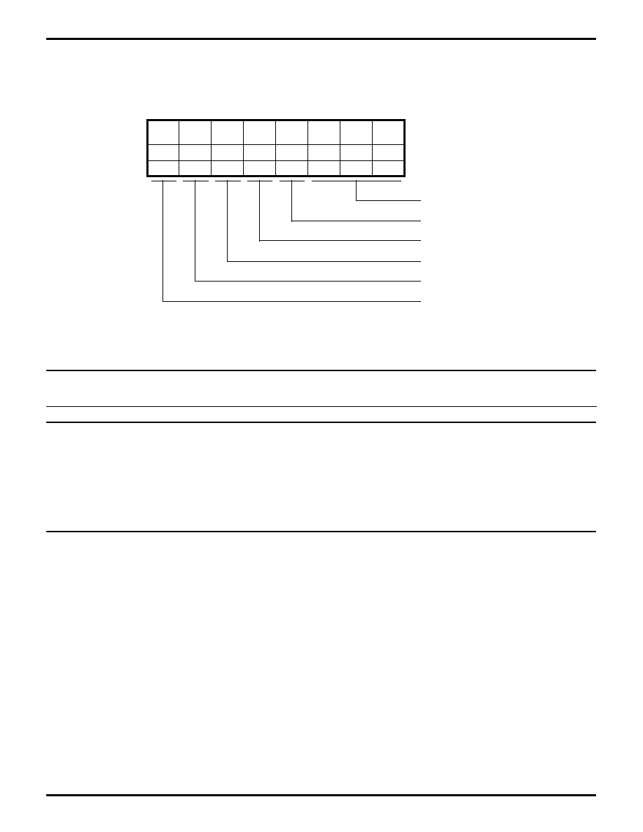
44
P R E L I M I N A R Y
Z80189/Z8L189
G
ENERAL
-P
URPOSE
E
MBEDDED
C
ONTROLLERS
DS971890301
Zilog
Z8S180 MPU REGISTERS
(Continued)
ASCI CHANNELS CONTROL REGISTERS
MPBT
MP
/CTS/
PS
SS2
SS1
SS0
Invalid
R/W
0
R/W
R/W
0
R/W
0
R/W
1
R/W
1
R/W
1
R/W
R/W
CNTLB0
Clock Source and Speed Select
Addr 02H
Bit
Upon Reset
DR
PE0
Divide Ratio
Parity Even or Odd
Clear To Send/Prescale
Multiprocessor
Multiprocessor Bit Transmit
/CTS - Depending on the condition of /CTS pin.
PS - Cleared to 0.
General
PS = 0
PS = 1
Divide Ratio
(Divide Ratio = 10)
(Divide Ratio = 30)
SS, 2, 1, 0
DR = 0 (x16)
DR = 1 (x64)
DR = 0 (x16)
DR = 1 (x64)
000
ÿ
˜
160
ÿ
˜
640
ÿ
˜
480
ÿ
˜
1920
001
ÿ
˜
320
ÿ
˜
1280
ÿ
˜
960
ÿ
˜
3840
010
ÿ
˜
640
ÿ
˜
2560
ÿ
˜
1920
ÿ
˜
7680
011
ÿ
˜
1280
ÿ
˜
5120
ÿ
˜
3840
ÿ
˜
15360
100
ÿ
˜
2560
ÿ
˜
10240
ÿ
˜
7680
ÿ
˜
30720
101
ÿ
˜
5120
ÿ
˜
20480
ÿ
˜
15360
ÿ
˜
61440
110
ÿ
˜
10240
ÿ
˜
40960
ÿ
˜
30720
ÿ
˜
122880
111
External Clock (Frequency < ÿ)
Figure 34. ASCI Control Register B (Ch. 0)

45
P R E L I M I N A R Y
Z80189/Z8L189
G
ENERAL
-P
URPOSE
E
MBEDDED
C
ONTROLLERS
DS971890301
Zilog
General
PS = 0
PS = 1
Divide Ratio
(Divide Ratio = 10)
(Divide Ratio = 30)
SS, 2, 1, 0
DR = 0 (x16)
DR = 1 (x64)
DR = 0 (x16)
DR = 1 (x64)
000
ÿ
˜
160
ÿ
˜
640
ÿ
˜
480
ÿ
˜
1920
001
ÿ
˜
320
ÿ
˜
1280
ÿ
˜
960
ÿ
˜
3840
010
ÿ
˜
640
ÿ
˜
2560
ÿ
˜
1920
ÿ
˜
7680
011
ÿ
˜
1280
ÿ
˜
5120
ÿ
˜
3840
ÿ
˜
15360
100
ÿ
˜
2560
ÿ
˜
10240
ÿ
˜
7680
ÿ
˜
30720
101
ÿ
˜
5120
ÿ
˜
20480
ÿ
˜
15360
ÿ
˜
61440
110
ÿ
˜
10240
ÿ
˜
40960
ÿ
˜
30720
ÿ
˜
122880
111
External Clock (Frequency < ÿ)
Figure 35. ASCI Control Register B (Ch. 1)
MPBT
MP
/CTS/
PS
SS2
SS1
SS0
Invalid
R/W
0
R/W
R/W
0
R/W
0
R/W
1
R/W
1
R/W
1
R/W
R/W
CNTLB1
Clock Source and Speed Select
Addr 03H
Bit
Upon Reset
DR
PE0
Divide Ratio
Parity Even or Odd
Read - Status of /CTS pin
Write - Select PS
Multiprocessor
Multiprocessor Bit Transmit
/CTS - Depending on the condition of /CTS pin.
PS - Cleared to 0.

46
P R E L I M I N A R Y
Z80189/Z8L189
G
ENERAL
-P
URPOSE
E
MBEDDED
C
ONTROLLERS
DS971890301
Zilog
ASCI CHANNELS CONTROL REGISTERS
(Continued)
Figure 36. ASCI Status Register
RDRF OVRN
CTS1E TDRE
TIE
0
R
0
R
0
R
0
R
0
R/W
R/W
1
R
0
R/W
R/W
STAT1
Transmit Interrupt Enable
Addr 05H
Bit
Upon Reset
RIE
FE
Transmit Data Register
Empty
/CTS1 Enable
Receive Interrupt Enable
Framing Error
Parity Error
PE
0
Over Run Error
Receive Data Register Full
Figure 37. ASCI Status Register (Ch. 1)
Upon Reset
RDRF OVRN
/DCD0 TDRE
TIE
0
R
0
R
0
R
0
R
0
R/W
R
R
0
R/W
R/W
STAT0
Transmit Interrupt Enable
Addr 04H
Bit
RIE
FE
Transmit Data Register
Empty
Data Carrier Detect
Receive Interrupt Enable
Framing Error
Parity Error
PE
Over Run Error
Receive Data Register Full
/DCD0 - Depending on the condition of /DCD0 Pin.
TDRE is reset to 0, when /CTSO input is high.
/CTS0 Pin = L: TDRE = 1
/CTS0 Pin = H: TDRE = 0
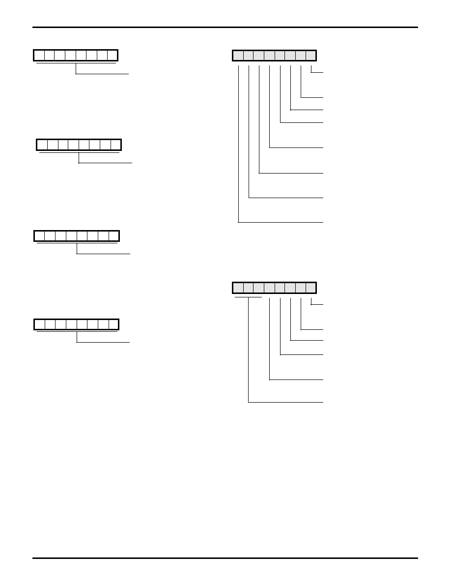
47
P R E L I M I N A R Y
Z80189/Z8L189
G
ENERAL
-P
URPOSE
E
MBEDDED
C
ONTROLLERS
DS971890301
Zilog
7
6
5
4
3
2
1
0
Transmit Data
TDR0
Write Only
Addr 06H
7
6
5
4
3
2
1
0
Transmit Data
TDR1
Write Only
Addr 07H
x
x
x
x
x
x
x
x
Received Data
TSR0
Read Only
Addr 08H
x
x
x
x
x
x
x
x
Received Data
TSR1
Read Only
Addr 09H
0
0
0
0
0
0
0
0
7
6
5
4
3
2
1
0
Reserved (Program as 0.)
DCD0 Disable
0 = DCD0 Auto-enables Rx
1 = DCD0 Advisory to SW
CTS0 Disable
0 = CTS0 Auto-enables Tx
1 = CTS0 Advisory to SW
X1 Bit CLK ASCIO
0 = CKA0 /16 or /64
1 = CKA0 is bit clock
BRG0 Mode
0 = as S180
1 = Enable 16-bit BRG Counter
Break Feature Enable
Break Detect (RO)
Send Break
0 = Normal Xmit
1 = Drive TXA Low
New Z8S180 Register
0
0
0
0
0
0
0
0
7
6
5
4
3
2
1
0
Break Feature Enable
Break Detect (RO)
Send Break
0 = Normal Xmit
1 = Drive TXA Low
BRG1 Mode
0 = As S180
1 = Enable 16-bit BRG Counter
X1 Bit CLK ASCI1
0 = CKA1 /16 or /64
1 = CKA1 is bit Clock
Reserved (Program as 0.)
New Z8S180 Register
Figure 38. ASCI Transmit Data Register (Ch. 0)
Figure 39. ASCI Transmit Data Register (Ch. 1)
Figure 40. ASCI Receive Data Register (Ch. 0)
Figure 41. ASCI Receive Data Register (Ch. 1)
Figure 43. ASCI1 Extension Control Register
(I/O Address 13)
Figure 42. ASCI0 Extension Control Register
(I/O Address 12)

48
P R E L I M I N A R Y
Z80189/Z8L189
G
ENERAL
-P
URPOSE
E
MBEDDED
C
ONTROLLERS
DS971890301
Zilog
ACSI TIME CONSTANT REGISTERS
New Z8S180 Registers
7
6
5
4
3
2
1
0
7
6
5
4
3
2
1
0
7
6
5
4
3
2
1
0
7
6
5
4
3
2
1
0
Register:
ASCI0 Time Constant High
Address:
1Bh
Register:
ASCI1 Time Constant Low
Address:
1Ch
Register:
ASCI1 Time Constant High
Address:
1Dh
Register:
ASCI0 Time Constant Low
Address:
1Ah
CLOCK MULTIPLIER REGISTER (Z180 MPU ADDRESS 1EH)
Bit 7.
X2 Clock Multiplier Mode. When this bit is set to 1, this
allows the programmer to double the internal clock from
that of the external clock. This feature will only operate
effectively with frequencies of 10-16 MHz (20-33 MHz
internal).
When this bit is set to 0, the Z189 device will operate in
normal mode. Upon powerup, this feature is disabled.
Bit 0-6
.
Reserved. Maintains a logic 1 value when read.
Figure 44. Clock Multiplier Register
(Z180 MPU Address 1EH)
New Z8S180 Register
0
1
1
1
1
1
1
1
Reserved
7
6
5
4
3
2
1
0
X2 Clock Multiplier Mode
0 = Disable
1 = Enable
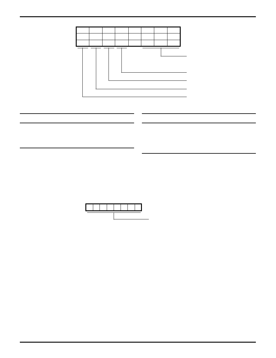
49
P R E L I M I N A R Y
Z80189/Z8L189
G
ENERAL
-P
URPOSE
E
MBEDDED
C
ONTROLLERS
DS971890301
Zilog
EF
EIE
SS2
SS1
SS0
0
R
0
R/W
0
R/W
0
R/W
1
1
R/W
1
R/W
1
R/W
R/W
Speed Select
Addr 0AH
Bit
Upon Reset
-
TE
Transmit Enable
Receive Enable
End Interrupt Enable
End Flag
RE
CNTR
SS2, 1, 0
Baud Rate
000
ÿ
˜
20
001
ÿ
˜
40
010
ÿ
˜
80
011
ÿ
˜
100
Figure 45. CSI/O Control Register
7
6
5
4
3
2
1
0
Read - Received Data
Write - Transmit Data
TRDR
Read/Write
Addr 0BH
Figure 46. CSI/O Transmit/Receive Data Register
SS2, 1, 0
Baud Rate
100
ÿ
˜
320
101
ÿ
˜
640
110
ÿ
˜
1280
111
External Clock
(Frequency < ÿ
˜
20)

50
P R E L I M I N A R Y
Z80189/Z8L189
G
ENERAL
-P
URPOSE
E
MBEDDED
C
ONTROLLERS
DS971890301
Zilog
TIMER DATA REGISTERS
7
6
5
4
3
2
1
0
TMDR0L
Read/Write
Addr 0CH
7
6
5
4
3
2
1
0
TMDR1L
Read/Write
Addr 14H
15 14 13 12 11 10 9
8
TMDR0H
Read/Write
Addr 0DH
When Read, read Data Register L
before reading Data Register H.
15 14 13 12 11 10 9
8
TMDR1H
Read/Write
Addr 15H
When Read, read Data Register L
before reading Data Register H.
Figure 47. Timer 0 Data Register L
Figure 48. Timer 1 Data Register L
Figure 49. Timer 0 Data Register H
TIMER RELOAD REGISTERS
7
6
5
4
3
2
1
0
RLDR0L
Read/Write
Addr 0EH
7
6
5
4
3
2
1
0
RLDR1L
Read/Write
Addr 16H
15 14 13 12 11 10 9
8
RLDR0H
Read/Write
Addr 0FH
15 14 13 12 11 10 9
8
RLDR1H
Read/Write
Addr 17H
Figure 51. Timer 0 Reload Register L
Figure 52. Timer 1 Reload Register L
Figure 53. Timer 0 Reload Register H
Figure 54. Timer 1 Reload Register H
Figure 50. Timer 1 Data Register H

51
P R E L I M I N A R Y
Z80189/Z8L189
G
ENERAL
-P
URPOSE
E
MBEDDED
C
ONTROLLERS
DS971890301
Zilog
TIMER CONTROL REGISTER
TIF1
TIF0
TOC0 TDE1 TDE0
0
R
0
R
0
R/W
0
R/W
0
R/W
R/W
0
R/W
0
R/W
R/W
TCR
Timer Down Count Enable 1,0
Addr 10H
Bit
Upon Reset
TOC1
TIE0
Timer Output Control 1,0
Timer Interrupt Enable 1,0
Timer Interrupt Flag 1,0
TIE1
0
TOC1,0 A15/TOUT
00
Inhibited
01
Toggle
10
0
11
1
Figure 55. Timer Control Register
52
P R E L I M I N A R Y
Z80189/Z8L189
G
ENERAL
-P
URPOSE
E
MBEDDED
C
ONTROLLERS
DS971890301
Zilog
FREE RUNNING COUNTER
7
6
5
4
3
2
1
0
FRC
Read Only
Addr 18H
Figure 56. Free Running Counter
CPU CONTROL REGISTER
The Z8S180 has an additional register which allows the
programmer to select options that directly affect the CPU
performance as well as controlling the STANDBY operat-
ing mode of the chip. The CPU Control Register (CCR)
allows the programmer to change the divide-by-two inter-
nal clock to divide-by-one. In addition, applications where
EMI noise is a problem, the Z8S180 can reduce the output
drivers on selected groups of pins to 33% of normal pad
driver capability which minimizes the EMI noise generated
by the part.
Figure 57. CPU Control Register
D7
D6
D5
D4
D3
D2
D1
D0
CPU Control Register (CCR) Addr 1FH
LNIO
0 = Standard Drive
1 = 33% Drive or
ASCI Signals
Standby/Idle Enable
00 = No Standby
01 = Idle After Sleep
10 = Standby After Sleep
11 = Standby After Sleep
64 Cycle Exit
(Quick Recovery)
0
0
0
0
0
0
0
0
LNAD/DATA
0 = Standard Drive
1 = 33% Drive On
A19-A0, D7-D0
LNCPUCTL
0 = Standard Drive
1 = 33% Drive On CPU
Control Signals
LNPHI
0 = Standard Drive
1 = 33% Drive On
EXT.PHI Clock
BREXT
0 = Ignore BUSREQ
In Standby/Idle
1 = Standby/Idle Exit
on BUSREQ
Clock Divide
0 = XTAL/2
1 = XTAL/1

53
P R E L I M I N A R Y
Z80189/Z8L189
G
ENERAL
-P
URPOSE
E
MBEDDED
C
ONTROLLERS
DS971890301
Zilog
Bit 7.
Clock Divide Select. Bit 7 of the CCR allows the
programmer to set the internal clock to divide the external
clock by 2 if the bit is 0 and divide-by-one if the bit is 1.
Upon reset, this bit is set to 0 and the part is in
divide-by-two mode. Since the on-board oscillator is not
guaranteed to operate above 20 MHz, an external source
must be used to achieve the maximum 33 MHz operation
of the part, i.e., an external clock at 66 MHz with 50% duty
cycle.
If an external oscillator is used in divide-by-one mode, the
minimum pulse width requirement must be satisfied.
Bits 6 and 3.
STANDBY/IDLE Enable. These two bits are
used for enabling/disabling the IDLE and STANDBY mode.
Setting D6, D3 to 0 and 1, respectively, enables the IDLE
mode. In the IDLE mode, the clock oscillator is kept
oscillating but the clock to the rest of the internal circuit,
including the CLKOUT, is stopped. The Z8S180 enters
IDLE mode after fetching the second opcode of a SLEEP
instruction, if the I/O STOP bit is set.
Setting D6, D3 to 1 and 0, respectively, enables the
STANDBY mode. In the STANDBY mode, the clock oscil-
lator is stopped completely. The Z8S180 enters STANDBY
after fetching the second opcode of a SLEEP instruction,
if the I/O STOP bit is set.
Setting D6, D3 to 1 and 1, respectively, enables the
STANDBY-QUICK RECOVERY mode. In this mode, its
operations are identical to STANDBY except that the clock
recovery is reduced to 64 clock cycles after the exit
conditions are gathered. Similarly, in STANDBY mode, the
Z8S180 enters STANDBY after fetching the second opcode
of a SLEEP instruction, if the I/O STOP bit is set.
Bit 5.
BREXT. This bit controls the ability of the Z8S180 to
honor a bus request during STANDBY mode. If this bit is
set to 1 and the part is in STANDBY mode, a BUSREQ is
honored after the clock stabilization timer is timed out.
Bit 4.
LNPHI. This bit controls the drive capability on the
PHI Clock output. If this bit is set to 1, the PHI Clock output
is reduced to 33% of its drive capability.
Bit 2.
LNIO. This bit controls the drive capability of the
external I/O pins of the Z80189/Z80L189. When this bit is
set to 1, the output drive capability of the following pins is
reduced to 33% of the original drive capability:
- CKS
- TxAI
- RxS/CTS1
- CKA0/DREQ0
- TxS
- TxA0
- CKAI/TEND0 - /RTS0
Bit 1.
LNCPUCTL. This bit controls the drive capability of
the CPU Control pins. When this bit is set to 1, the output
drive capability of the following pins is reduced to 33% of
the original drive capability:
- /BUSACK
- /MREQ
- TEST
- /RD
- /IORQ
- STATUS
- /WR
- /RFSH
- /M1
- /HALT
- E
- /TEND1
Bit 0.
LNAD/DATA. This bit controls the drive capability of
the Address/Data bus output drivers. If this bit is set to 1,
the output drive capability of the Address and Data bus
output is reduced to 33% of its original drive capability.
54
P R E L I M I N A R Y
Z80189/Z8L189
G
ENERAL
-P
URPOSE
E
MBEDDED
C
ONTROLLERS
DS971890301
Zilog
DMA REGISTERS
BCR0L
Read/Write
Addr 26H
BC7
BC0
BCR0H
Read/Write
Addr 27H
BC15
BC8
MAR1L
Read/Write
Addr 28H
MA7
MA0
MAR1H
Read/Write
Addr 29H
MA15
MA8
MAR1B
Read/Write
Addr 2AH
MA16
MA19
-
-
-
-
Figure 58. DMA 0 Source Address Registers
Figure 60. DMA 0 Byte Counter Registers
Figure 61. DMA 1 Memory Address Registers
Figure 59. DMA 0 Destination Address Registers
SAR0L
Read/Write
Addr 20H
SA7
SA0
SAR0H
Read/Write
Addr 21H
SA15
SA8
SAR0B
Read/Write
Addr 22H
SA16
SA19
-
-
-
-
Bits 0-2 (3) are used for SAR0B
A19,
x
x
x
x
A18,
x
x
x
x
A17,
0
0
1
1
A16
0
1
0
1
DMA Transfer Request
ext (CKA0//DREQ0
ASCI0 Rx
ASCI1 Rx
ext (/DREQ1)
DAR0L
Read/Write
Addr 23H
DA7
DA0
DAR0H
Read/Write
Addr 24H
DA15
DA8
DAR0B
Read/Write
Addr 25H
DA16
DA19
-
-
-
-
Bits 0-2 (3) are used for DAR0B
A19,
x
x
x
x
A18,
x
x
x
x
A17,
0
0
1
1
A16
0
1
0
1
DMA Transfer Request
ext (CKA0//DREQ0)
ASCI0 Tx
ASCI1 Tx
ext (/DREQ1)

55
P R E L I M I N A R Y
Z80189/Z8L189
G
ENERAL
-P
URPOSE
E
MBEDDED
C
ONTROLLERS
DS971890301
Zilog
BCR1L
Read/Write
Addr 2EH
BC7
BC0
BCR1H
Read/Write
Addr 2FH
BC15
BC8
IAR1L
Read/Write
Addr 2BH
IA7
IA0
IAR1H
Read/Write
Addr 2CH
IA15
IA8
Figure 64. DMA I/O Address Register Ch. 1
Figure 63. DMA 1 Byte Count Registers
Figure 62. DMA I/O Address Registers
D7
D6
D5
D4
D3
D2
D1
D0
Alternating Channels
0 = DMA Channels
are independent
1 = Toggle between DMA
channels for same device
Currently selected DMA
Channel when Bit 7 = 1
Reserved, program as 0.
000 = DMA1 ext TOUT/DREQ
001 = DMA1 ASCI0
010 = DMA1 ASCI1
011 = DMA1 ext CKA0//DREQ0
111 = Reserved, do not program
IAR1B
Addr 2D
New Z8S180 Register

56
P R E L I M I N A R Y
Z80189/Z8L189
G
ENERAL
-P
URPOSE
E
MBEDDED
C
ONTROLLERS
DS971890301
Zilog
DMA REGISTER DESCRIPTION
Bit 7.
This bit should be set to 1 only when both DMA
channels are set to take their requests from the same
device. If this bit is 1 (it resets to 0), the TEND output of DMA
channel 0 sets a flip-flop, so that thereafter the device's
request is visible to channel 1, but is not visible to channel
0. The internal TEND signal of channel 1 clears the FF, so
that thereafter, the device's request is visible to channel 0,
but not visible to channel 1.
If DMA requests are from differing sources, DMA channel
0 request will be forced onto DMA channel 1 once TEND
output of DMA channel 0 sets the flop-flop to alternate.
Bit 6.
When both DMA channels are programmed to take
their requests from the same device, this bit (FF mentioned
in the previous paragraph) controls which channel the
device's request is presented to: 0 = DMA 0, 1 = channel
1. When bit 7 is 1, this bit is automatically toggled by the
channel end output of the channels, as described above.
Bits 5-3.
Reserved and should be programmed as 0.
Bits 2-0.
With "DIM1", bit 1 of DCNTL, these bits control
which request is presented to DMA channel 1, as follows:
DIM1 IAR18-16
Request Routed to DMA Channel 1
0
000
/DREQ1
0
001
ASCI0 Tx
0
010
ASCI1 Tx
0
011
ext CKA0//DREQ0
0
10X
Reserved, do not program.
0
1X0
Reserved, do not program.
0
111
Reserved, do not program
1
000
ext /DREQ1
1
001
ASCI0 Rx
1
010
ASCI1 Rx
1
011
ext CKA0//DREQ0
1
10X
Reserved, do not program.
1
1X0
Reserved, do not program.
1
111
Reserved, do not program
57
P R E L I M I N A R Y
Z80189/Z8L189
G
ENERAL
-P
URPOSE
E
MBEDDED
C
ONTROLLERS
DS971890301
Zilog
DE1
DE0
DIE0
-
DIME
0
R/W
0
R/W
1
W
1
W
0
0
R/W
1
0
R
R/W
DMA Master Enable
Addr 30H
Bit
Upon Reset
DIE1
/DWE0
DMA Interrupt Enable 1, 0
DMA Enable Bit Write Enable 1, 0
DMA Enable Ch 1, 0
/DWE1
DSTAT
R/W
Figure 65. DMA Status Register
-
-
SM0
MMOD
-
1
1
0
R/W
0
R/W
0
0
R/W
0
1
R/W
Memory MODE Select
Addr 31H
Bit
Upon Reset
SM1
DM0
Ch 0 Source Mode 1, 0
Ch 0 Destination Mode 1, 0
DM1
DMODE
R/W
R/W
DM1, 0
00
01
10
11
Destination
M
M
M
I/O
Address
DAR0+1
DAR0-1
DAR0 Fixed
DAR0 Fixed
SM1, 0
00
01
10
11
Source
M
M
M
I/O
Address
SAR0+1
SAR0-1
SAR0 Fixed
SAR0 Fixed
0
1
Mode
Cycle Steal Mode
Burst Mode
MMOD
Figure 66. DMA Mode Registers
58
P R E L I M I N A R Y
Z80189/Z8L189
G
ENERAL
-P
URPOSE
E
MBEDDED
C
ONTROLLERS
DS971890301
Zilog
DMA REGISTERS
(Continued)
MWI1
MWI0
DMS0
DIM1
DIM0
1
1
1
R/W
1
R/W
0
0
R/W
0
0
R/W
DMA Ch 1 I/O Memory
Mode Select
Addr 32H
Bit
Upon Reset
DMS1
IWI0
/DREQi Select, i = 1, 0
I/0 Wait Insertion
IWI1
DCNTL
R/W
R/W
R/W
R/W
R/W
Memory Wait Insertion
DM1, 0
00
01
10
11
Transfer Mode
M - I/O
M - I/O
I/O - M
I/O - M
Address Increment/Decrement
DMSi
1
0
Sense
Edge Sense
Level Sense
MWI1, 0
00
01
10
11
No. of Wait States
0
1
2
3
IWI1, 0
00
01
10
11
No. of Wait States
1
2
3
4
MAR1+1
MAR1-1
IAR1 Fixed
IAR1 Fixed
IAR1 Fixed
IAR1 Fixed
MAR1+1
MAR1-1
*
Note:
* If using ROM/RAM Chip Select wait state generators,
the Z180 wait state generator should be set to 0.
Figure 67. DMA/WAIT Control Register

59
P R E L I M I N A R Y
Z80189/Z8L189
G
ENERAL
-P
URPOSE
E
MBEDDED
C
ONTROLLERS
DS971890301
Zilog
SYSTEM CONTROL REGISTERS
IL7
IL6
-
-
-
0
0
0
R/W
0
0
0
0
0
R/W
Interrupt Vector Low
Addr 33H
Bit
Upon Reset
-
-
IL5
IL
R/W
R/W
REFE REFW
-
CYC1 CYC0
1
1
1
1
1
1
0
0
R/W
Cycle Select
Addr 36H
Bit
Upon Reset
-
-
Refresh Wait State
Refresh Enable
-
RCR
R/W
R/W
R/W
R/W
CYC1, 0
00
01
10
11
Interval of Refresh Cycle
10 states
20 states
40 states
80 states
TRAP UFO
ITE2
ITE1
ITE0
0
0
1
1
1
0
R/W
0
1
R/W
/INT Enable 2, 1, 0
Addr 34H
Bit
Upon Reset
-
-
-
ITC
R/W
R
R/W
R/W
Undefined Fetch Object
TRAP
Figure 69. INT/TRAP Control Register
Figure 70. Refresh Control Register
Figure 68. Interrupt Vector Low Register
60
P R E L I M I N A R Y
Z80189/Z8L189
G
ENERAL
-P
URPOSE
E
MBEDDED
C
ONTROLLERS
DS971890301
Zilog
MMU REGISTERS
CB7
CB6
CB2
CB1
CB0
0
0
0
R/W
0
R/W
0
0
R/W
0
0
R/W
MMU Common Base
Register
Addr 38H
Bit
Upon Reset
CB3
CB4
CB5
CBR
R/W
R/W
R/W
R/W
R/W
BB7
BB6
BB2
BB1
BB0
0
0
0
R/W
0
R/W
0
0
R/W
0
0
R/W
MMU Bank Base Register
Addr 39H
Bit
Upon Reset
BB3
BB4
BB5
BBR
R/W
R/W
R/W
R/W
R/W
CA3
CA2
BA2
BA1
BA0
1
1
1
R/W
1
R/W
0
0
R/W
0
0
R/W
MMU Bank Area Register
Addr 3AH
Bit
Upon Reset
BA3
CA0
CA1
CBAR
R/W
R/W
R/W
R/W
R/W
MMU Common Area Register
Figure 72. MMU Bank Base Register
Figure 71. MMU Common Base Register
Figure 73. MMU Common/Bank Area Register

61
P R E L I M I N A R Y
Z80189/Z8L189
G
ENERAL
-P
URPOSE
E
MBEDDED
C
ONTROLLERS
DS971890301
Zilog
SYSTEM CONTROL REGISTERS
IOA7
IOA6
-
-
-
0
0
0
1
1
1
1
1
R/W
I/O Stop
Addr 3FH
Bit
Upon Reset
-
-
I/O Address
Combination of 11
is reserved
IOSTP
ICR
R/W
R/W
R/W
M1E /M1TE
-
-
-
1
1
1
1
1
1
1
1
R/W
I/O Compatibility
Addr 3EH
Bit
Upon Reset
-
-
/M1 Temporary Enable
/M1 Enable
/IOC
OMCR
W
R/W
R/W
Notes:
1. This register should be programmed to 0x0xxxxxb
(x = don't care) as a part of Initialization.
2. If the M1E bit is set to 1, the processor does not
fetch a RETI instruction.
Figure 74. Operation Mode Control Register
Figure 75. I/O Control Register

62
P R E L I M I N A R Y
Z80189/Z8L189
G
ENERAL
-P
URPOSE
E
MBEDDED
C
ONTROLLERS
DS971890301
Zilog
Z80189 MIMIC REGISTER MAP
Register Name
MPU Addr/Access
PCAddr/Access
MMC MIMIC Master Control Reg.
XXFF R/W
None
IUS/IP Interrupt Pending
XXFE R/Wb7
None
IE Interrupt Enable
XXFD R/W
None
IVEC Interrupt Vector
XXFC R/W
None
RTCR Receive Time Constant
XXFB R/W
None
TTCR Transmit Time Constant
XXFA R/W
None
DLM Divisor Latch (MSByte)
XXF9 R only
01,DLAB=1,R/W
DLL Divisor Latch (LSByte)
XXF8R only
00,DLAB=1,R/W
SCR Scratch Register
XXF7 R only
07 R/W
MSR Modem Status Register
XXF6 R/Wb7-4
06 R only
LSR Line Status Register
XXF5 R/Wb6432
05 R only
MCR Modem Control Register
XXF4 R only
04 R/W
LCR Line Control Register
XXF3 R only
03 R/W
IER Interrupt Enable Register
XXF1 R only
01,DLAB=0 R/W
RBR Receiver Buffer Register
XXF0 W only
00,DLAB=0 R only
THR Transmitter Holding Reg.
XXF0 R only
00,DLAB=0 W only
FSCR FIFO Status and Control
XXEC R/W7-4
None
TTTC Tran. Timeout Time Const.
XXEB R/W
None
RTTC Rec. Timeout Time Const.
XXEA R/W
None
IIR Interrupt Identification
None
02 R only
FCR FIFO Control Register
XXE9 R only
02 W only
Z80189 PC DMA MAILBOX BRG,COM_PORT, PIA AND MISC REGISTERS
Register Name
MPU Addr/Access
PCAddr/Access
PA Data Direction Register
XXEDH R/W
None
PA Data Register
XXEEH R/W
None
MIMIC Modification Register
XXE9 W only
None
ROM Address Boundary Reg.
XXE8 R/W
None
RAMLBR RAM Lower Boundary Reg.
XXE7 R/W
None
RAMUBR RAM Upper Boundary Reg.
XXE6 R/W
None
PB Data Register
XXE5 R/W
None
PB Data Direction Register
XXE4 R/W
None
BRG High Constant
XXE1 R/W
None
BRG Low Constant
XXE0 R/W
None
Interrupt Edge/Pin Mux Control
XXDF R/W
None
PC Data Register
XXDE R/W
None
PC Data Direction Register
XXDD R/W
None
Z80189 Enhancements Register
XXD9 R/W
None
WSG Chip Select Register
XXD8 R/W
None
IOBRG Register
XXD6 R/W
None
COM Decode Register
XXD7 R/W
None
System Configuration Register
XXEF R/W
None

63
P R E L I M I N A R Y
Z80189/Z8L189
G
ENERAL
-P
URPOSE
E
MBEDDED
C
ONTROLLERS
DS971890301
Zilog
Z80189 MAILBOX REGISTER MAP
Register Name
MPU Addr/Access
PC Addr/Access
Host I/O Status Register
%XXD5 W bit 1/R
Prog + 10b R (2)
Host Output Register 1
%XXD4 R
Prog + 01b W (2)
Host Input Register 1
%XXD4 W
Prog + 01b R (2)
Host Output Register 0
%XXD3 R
Prog + 00b W (2)
Host DMA Mailbox Cntrl Reg
%XXD2 R/W
None
Host DMA Transmit Register 1
%XXD1 R
DMA1 W (3)
Host DMA Receive Register 1
%XXD1 W
DMA1 R
Host DMA Transmit Register 0
%XXD0 R (1)
DMA0 W
Host DMA Receive Register 0
%XXD0 W
DMA0 R
1.
This register is defaulted to 91h to indicate revision code.
(Z189 revision #1 - Z80189AA)
2.
The PC Host Addresses are HA9:2 are programmable by writing to PADATA.
3.
The HDMAT1 can be used as an extra host output mailbox register. If the Host DMA Mailbox 1 function is disabled
(bit 1 of HMC register is zero), a Host write in the programmed Mailbox range with HA1, 0=1,1 will cause the host data
to be latched into the HDMAT1 register.
Note:
All register addresses not listed are Reserved.
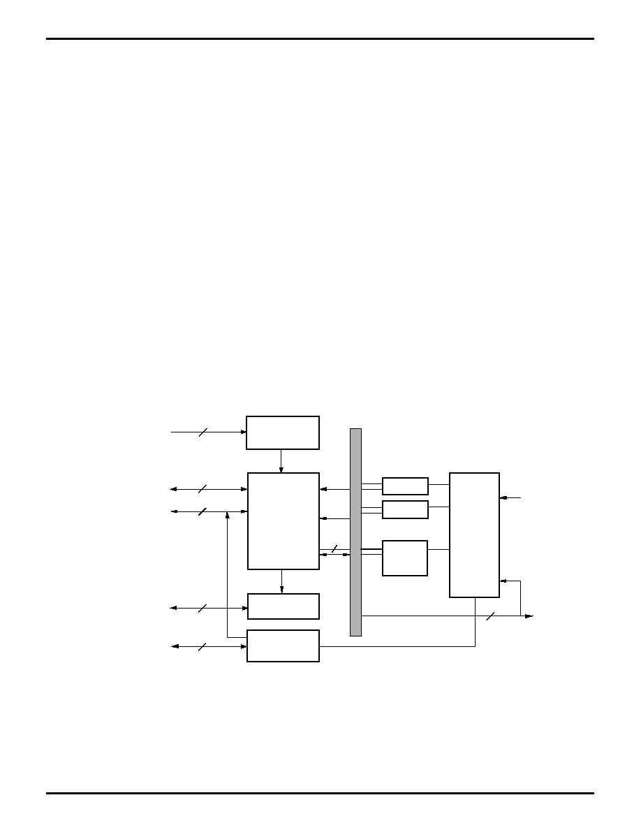
64
P R E L I M I N A R Y
Z80189/Z8L189
G
ENERAL
-P
URPOSE
E
MBEDDED
C
ONTROLLERS
DS971890301
Zilog
16550 MIMIC INTERFACE
The Z80189 has a 16550 MIMIC interface that allows it to
mimic the 16550 device. It has all the interface pins
necessary to connect up to the PC/XT/AT bus without any
extra circuitry. It contains the complete register set of the
16550 part with the same interrupt structure. The data path
allows parallel transfer of data to and from the register set
by the internal Z80180 of the Z80189. There is no shift
register associated with the MIMIC of the 16550 UART.
This interface saves the application from doing a serial
transfer before performing data compression or error
correction on the data.
Control of the register set is maintained by six priority
encoded interrupts to the Z80189. When the PC/XT/AT
writes to THR, MCR, LCR, DLL, DLM, FCR or reads the
RBR, an interrupt to the Z80189 is generated. Each inter-
rupt can be individually masked off or all interrupts can be
disabled by writing a single bit. Both mode 0, mode 1 and
mode 2 interrupts are supported by the 16550 MIMIC
interface.
Two 8-bit timers are also available to control the data
transfer rate of the 16550 MIMIC interface. Their input is
tied to the BRG clock so a down count of 24 bits is possible.
An additional two 8-bit timers are available for program-
ming the FIFO time-out feature (4 Character Time Emula-
tion) for both Receiver and Transmitter FIFO's.
The 16550 MIMIC interface supports the PC/XT/AT inter-
rupt structure as well as an additional mode that allows for
a wired AND interrupt structure.
All registers of the 16550 MIMIC interface are accessible
in any page of I/O space since only the lowest 8 address
lines are decoded.
COM Port Decode functionality is integrated into the Z189.
This allows the MIMIC to be selected for a specific COM
Port Address (PC COM Port Address 1-4). Previously for
the Z80182, the COM Port Address selected for the MIMIC
was implemented through external COM Port Decode
circuitry. The COM Port Decode circuitry in the Z80189
simplifies this process by allowing the user to select the
MIMIC Com Port addresses through software, as well as
reducing the system board level costs by saving board
space and external circuitry.
See Figure 76 for a block diagram of the 16550 MIMIC
interface.
Figure 76. 16550 MIMIC Block Description
16550 MIMIC
Register Set
4
8
Host Addr Decode
Host Data Bus
Rx Timer
Z80180
IRQ &
Control
180 Side
Control
Config
Register
D
A
T
A
B
U
S
Z80180
Address
PC Host IRQ
8
Z80180 Data Bus
6
PC IRQ
1
PC DMA Mailbox
and I/O Mailbox
PC DMA Control
Selectable
COM Port Decode
10
PC Side
4
Tx Timer

65
P R E L I M I N A R Y
Z80189/Z8L189
G
ENERAL
-P
URPOSE
E
MBEDDED
C
ONTROLLERS
DS971890301
Zilog
16550 MIMIC FIFO DESCRIPTION
The receiver FIFO consists of a 16-word FIFO capable of
storing eight data bits and three error bits for each charac-
ter stored (Figure 77). Parity error, Framing error and Break
detect bits are stored, along with the data bits, by copying
their value from three shadow bits, which are write only bits
for the Z80180 MPU LSR address. The three shadow bits
are cleared after they are copied to the FIFO memory. In
FIFO mode, to write error bits into the receiver FIFO, the
MPU must first write the Parity, Framing and Break detect
status to the Line Status Register (shadow bits) and then
write the character associated into the receiver buffer. The
data and error bits will then move into the same address in
the FIFO. The error bits become available to the PC side of
the interface when that particular location becomes the
next address to read (top of FIFO). At that time they may
either be read by the PC by accessing them in the LSR, or
they may cause an interrupt to the PC interface if so
enabled. The error bits are set by the error status of the byte
at the top of the FIFO but may only be cleared by reading
the LSR. If successive reads of the receiver FIFO are
performed without reading the LSR, the status bits will be
set if any of the bytes read have the respective error bit set.
The PC interface may be interrupted when 1, 4, 8 or 14
bytes are available in the receiver FIFO by setting bits 6
and 7 in the FCR (FIFO Control Register, PC address 02h
to the appropriate value. If the FIFO is not empty, but below
the above trigger value, a time-out interrupt is available if
the receiver FIFO is not written by the MPU or read by the
PC by an interval determined by the Character Time-out
Timer. This is an additional Timer with MPU access only
which is used to emulate the 16550 4 character time-out
delay. The timer receives the BRG as its input clock.
Software must determine the correct values to program
into the Receiver Time-out register and the BRG to achieve
the correct delay interval for time-out. These interrupts are
cleared by the FIFO reaching the trigger point or by
resetting the Time-out interval timer by FIFO MPU write or
PC read access.
With FIFO mode enabled, the MPU is interrupted when the
receiver FIFO is empty, corresponding to bit 5 being set in
the IUS/IP register (MPU access only). This bit corre-
sponds to a PC read of the receiver buffer in non-FIFO
(16450) mode. The interrupt source is cleared when the
FIFO becomes non-empty or the MPU reads the IUS/IP
register.
The transmitter FIFO is a 16 byte FIFO with PC write and
MPU read access (Figure 78). In FIFO mode, the PC will
receive an interrupt when the transmitter becomes empty
corresponding to bit 5 being set in the LSR. This bit and the
interrupt source are cleared when the transmitter FIFO
becomes non-empty or the IIR register is read by the PC.
On the MPU interface, the transmitted data available can
be programmed to interrupt the MPU on 1, 4, 8 or 14 bytes
of available data by seeing the appropriate value in the
MPU FSCR control register (MPU write only XXECH) bits 6
and 7. A time-out feature exists, Transmitter Time-out
Timer, which is an additional 8 bit timer with BRG as the
input source. If the transmitter FIFO is non-empty and no
PC write or MPU read of the FIFO has taken place within the
timer interval, a time-out will occur causing a correspond-
ing interrupt to the MPU.

66
P R E L I M I N A R Y
Z80189/Z8L189
G
ENERAL
-P
URPOSE
E
MBEDDED
C
ONTROLLERS
DS971890301
Zilog
16550 MIMIC FIFO DESCRIPTION
(Continued)
W
R
I
T
E
B
U
F
F
E
R
16x8
Data Bits
16x3
Error
Bits
R
E
A
D
B
U
F
F
E
R
Write
Pointer
ALU
Read
Pointer
Sync
phi
MPU_RD
PC Read
LSR
B2-B4
error
3
3
MPU Write
LSR Shadow
B2-B4
8
MPU
Databus
(MPU Side Write)
Sync
8
5
PC Side
Databus
(PC Side Read)
FIFO Control
Register
PC
IRQ
PC_RD
phi
MPU Side
Interface
16550
MIMIC or
PC Side
Interface
phi
MPU
IRQ
Figure 77. Receiver FIFO Block Diagram

67
P R E L I M I N A R Y
Z80189/Z8L189
G
ENERAL
-P
URPOSE
E
MBEDDED
C
ONTROLLERS
DS971890301
Zilog
Figure 78. Transmitter FIFO Block Diagram
W
R
I
T
E
B
U
F
F
E
R
16x8
Data Bits
R
E
A
D
B
U
F
F
E
R
Write
Pointer
ALU
Sync
phi
PC_WR
8
phi
PC
IRQ
Sync
8
MPU Read
(Data)
FCR Reg.
MPU
IRQ
MPU_RD
phi
16550
MIMIC or
PC side
interface
16550
MIMIC or
PC Side
Interface
Read
Pointer
5
PC
Write

68
P R E L I M I N A R Y
Z80189/Z8L189
G
ENERAL
-P
URPOSE
E
MBEDDED
C
ONTROLLERS
DS971890301
Zilog
16550 MIMIC FIFO DESCRIPTION
(Continued)
Table 15. 16550 Line Status Register
Error
Description
How to Set
How to Clear
Error in
At least one data byte available
At least one error in receiver
When there are no more
RCVR
in FIFO with one error
FIFO
errors
FIFO
*TEMT
Transmitter empty
MPU writes a 1
MPU writes a 0
*THRE
Transmitter holding
When MPU has
When holding register
register is empty
read or emptied
is not empty
the holding register
Break
Break occurs when
MPU writes 1
There is a
Detect
received data input
PC-side read
is held in logic-0
of the LSR
for longer than a
full word transmission
Framing
Received character
MPU writes 1
There is a
Error
did not have a valid
PC-side read
stop bit
of the LSR
Parity
Received character
MPU writes 1
There is a
Error
did not have correct
PC-side read
even or odd parity
of the LSR
Overrun
Overlapping received
MPU makes
There is a
Error
characters, thereby
two writes
PC-side read
destroying the
to receiver
of the LSR
previous character
buffer register
Data
Indicates complete
MPU writes to
Empty Receiver
Ready
incoming data has
RCVR FIFO or
or Receiver FIFO
been received
receiver buffer
register
Notes:
* The TEMT and THRE bits take on different functions when
TEMT/Double Buffer mode is enabled.
These signals are delayed to HOST when using character
emulation delay.

69
P R E L I M I N A R Y
Z80189/Z8L189
G
ENERAL
-P
URPOSE
E
MBEDDED
C
ONTROLLERS
DS971890301
Zilog
Z80189 MIMIC SYNCHRONIZATION CONSIDERATIONS
Because of the asynchronous nature of the FIFO's on the
MIMIC, some scheme of synchronization must be pro-
vided to prevent conflict from the dual port accesses of the
MPU and the PC.
To solve this problem, I/O to the FIFO is buffered, the
buffers allowing both PC and MPU to access the FIFO
asynchronously. Read and Write requests are then syn-
chronized by means of the MPU clock. Incoming signals
are buffered in such a way that meta-stable input levels will
be stabilized to valid 1 or 0 levels. Actual transfers to and
from the buffers from and to the FIFO memory are timed by
the MPU clock. ALU evaluation is performed on a different
phase than the transfer to ensure stable pointer values.
Another potential problem is that of simultaneous access
of the MPU and PC to any of the various `mailbox' type
registers. This is solved by dual buffering of the various
read/write registers. During a read access by either MPU
or PC to a mailbox register, the data in the buffered slave
register is not permitted to change. Any write that might
take place during this time will be stored in the input of the
master register. The corresponding status/interrupt will be
reset as appropriate based on the write having followed
the read to the register. For example, the IUS/IP bit for the
LCR write will not be cleared by the MPU read of the LCR
if a simultaneous write to the LCR by the PC takes place.
Instead the LSR data will change after the read access and
IUS/IP bit 3 will remain at logic 1.
DOUBLE BUFFERING FOR THE TRANSMITTER IN 16450 MODE
The Z80189 implements double buffering for the transmit-
ter in 16450 mode and sets the TEMT bit in the LSR
Register automatically.
If character delay emulation is being used (see Figure 79):
1.
The PC THRE bit in the LSR Register is set when the
THR Register is empty;
2.
PC Host writes to the 16450 THR Register;
3.
Whenever the Z80189 TSR buffer is empty and one
character delay timer is in a time out state, the byte
from the THR Register is transferred to the TSR buffer;
4.
Restart character delay timer (timer reloads and counts
down) with byte transfer from THR Register to the TSR
buffer;
5.
Whenever the TSR buffer is full, the TEMT bit in LSR
Register for MPU is reset with no delay;
6.
MPU reads TSR buffer;
7.
TEMT bit in LSR Register for MPU is set with no delay
whenever the TSR buffer is empty;
8.
When the TSR buffer is read by MPU and THR Register
is empty and one character delay timer reaches zero
the TEMT bit in the LSR Register for Host is set from 0
to 1.
The PC THRE bit in the LSR Register is reset whenever the
THR Register is full and set whenever THR Register is
empty. MPU IREQ and DMA Request for the transmit data
is triggered whenever the TSR buffer is full and cleared
whenever TSR buffer is empty.
If character delay emulation is not used the TEMT bit in the
LSR Register is set whenever both the THR Register and
the TSR buffer are both empty. The Host TEMT bit is clear
if there is data in either the TSR buffer or THR Register.
Disable this feature when 16550 FIFO mode is enabled.

70
P R E L I M I N A R Y
Z80189/Z8L189
G
ENERAL
-P
URPOSE
E
MBEDDED
C
ONTROLLERS
DS971890301
Zilog
DOUBLE BUFFERING FOR THE TRANSMITTER IN 16450 MODE
(Continued)
16450
THR
Register
Host Write
Empty/Full
Host & MPU THRE = 1 0
Byte Transfer if:
- THRE=0; and
- TSRE = 1; and
- Character delay timer is timed out.
Note: Timer reloads and counts down
whenever data is transferred from THR to TSR.
THR to TSR
delay
transfer
TSR
Transmit
Shift Reg.
Emulation
Empty/Full
(MPU TEMT) TSRE = 1 0
Host TEMT = 1 if - THRE = 1 and
- TSRE = 1 and
- Emulation delay timer is timed out
Note: MPU sees TSR bit in the LSR Register as TEMT bit
Added TSR Buffer for the
transmit data
Z80189 MIMIC DMA Consideration
Since the /HRXRDY and /HTXRDY is removed in the Z189,
the MIMIC DMA feature found on the Z182 is not available
on the Z189.
Z80189 MIMIC Design Hint
The MIMIC output drive capability has been increased to
16 mA on the Z189. This may eliminate the need for
buffering to the PC Bus.
Figure 79. TEMT Emulation Logic Implementation

71
P R E L I M I N A R Y
Z80189/Z8L189
G
ENERAL
-P
URPOSE
E
MBEDDED
C
ONTROLLERS
DS971890301
Zilog
16550 MIMIC INTERFACE REGISTERS
The 16550 MIMIC interface is controlled by the MMC
register. Setting it allows for different modes of operation
such as using the eight bit counters and which IRQ
structure is used with the PC/XT/AT.
Both counters are single pass and stop on a count of zero.
Their purpose is to delay data transfer just as if the 16550
UART had to shift the data in and out. This is provided to
alleviate any software problems a high speed continuous
data transfer might cause to existing software. If this is not
a problem, then data can be read and written as fast as the
two machines can access the devices. In FIFO mode of
operation, the timers are used to delay the status to the PC
interface by the time that would be required to actually shift
the characters out or in if an actual UART were present.
Bit 5 Reserved as 0
Bit 4 Reserved as 0
Bit 3 Reserved as 0
Bit 2,1 Interrupt Select (Read/Write)
Bits 2, 1
00
If both bits 2 and 1 are set to zero, then the active
HINTR1 pin is set to normal 16550 MIMIC mode.
01
If bit 2 is zero and bit 1 is one, then the 16550
MIMIC will enable a wire AND condition on the
active HINTR1 pin to the PC/XT/AT.
10
If bit 2 is one and bit 1 is zero, then the active
HINTR1 pin will be driven only if out 2 of the
Modem Control register is a one. If out 2 is a zero,
then the active HINTR1 pin will be tri-stated.
11
Both bits should never be set to one. This is a
reserved condition and should not be used.
Bit 0 Vector Include Status (Read/Write)
This bit is used to select the interrupt response mode of the
Z180. A 0 in this bit enables mode 0 interrupts; a 1 enables
mode 2 response.
0
0
0
0
0
0
0
0
VIS Vector Include Status
0 = Mode 0 Interrupts
1 = Mode 2 Interrupts
7
6
5
4
3
2
1
0
HINTR1
00 = Normal
01 = Wire And
10 = Out 2 Control
11 = Reserved
Reserved as 0
Reserved as 0
Reserved as 0
Rx Timer Enable
Tx Timer Enable
Figure 80. MIMIC Master Control Register
(Z180 MPU Address XXFFH)
Bit 7 Transmit Timer Delay Counter
Enable (Read/Write)
If bit 7 is set to a one, it enables the transmit delay timer.
When the Z180 reads the Transmit Register, the transmit
delay timer is automatically loaded with the Transmit Time
Constant Register and the timer is enabled to countdown
to zero. This timer delays setting the Transmitter Holding
Register Empty (THRE) bit until the timer times out. If this
bit is zero, then THRE is set immediately on a Z180 read of
the Transmit Register.
Bit 6 Receive Timer Delay Counter
Enable (Read/Write)
If bit 6 is set to a one, it enables the receive delay timer.
When the Z180 writes to the Receive Buffer, it loads the
receive delay timer from the Receive Time Constant Reg-
ister and enables the timer to countdown to zero. This timer
delays setting the Data Ready (DR) bit in the LSR until the
timer times out. If this bit is a zero, then DR is set immedi-
ately on a Z180 write to the Receive Buffer.

72
P R E L I M I N A R Y
Z80189/Z8L189
G
ENERAL
-P
URPOSE
E
MBEDDED
C
ONTROLLERS
DS971890301
Zilog
16550 MIMIC INTERRUPT REGISTERS
IUS/IP Register
The IUS/IP Register is used by the Z180 MPU to determine
what has caused the Interrupt. This register will have the
appropriate bit set when an interrupt occurs.
Bit 5 Transmitter Time-out with Data in FIFO
(Read Only)
This bit is set when the transmitter FIFO has been idle (no
read or write and timer decrements to zero) with data bytes
below the trigger level. It is cleared when the FIFO is read
or written.
Bit 4 Receive Buffer Read (Read Only)
This bit is set when the PC/XT/AT reads the Receive Buffer
Register. It is reset when the Z180 MPU writes to the
Receive Buffer Register. In FIFO mode, this bit is set upon
the PC reading all the data in the receiver FIFO. Note: RBR
is set and interrupts when the receiver FIFO has been
emptied by the PC. This bit and interrupt are cleared when
one or more bytes are written into the receiver FIFO by the
MPU.
Bit 3 Modem Control Register Write (Read Only)
This bit is set when the PC/XT/AT writes to the Modem
Control Register. It is reset when the Z180 MPU reads the
Modem Control Register.
Bit 2 Line Control Register Write (Read Only)
This bit is set when the PC/XT/AT writes to the Line Control
Register. It is reset when the Z180 MPU reads the Line
Control Register.
Bit 1 Divisor Latch LS/MS Write (Read Only)
This bit is set when the PC/XT/AT writes to the Divisor Latch
Least Significant or Most Significant bytes. It is reset when
the PC reads the LS/MS register(s). To determine which
byte(s) have been written, the Z180 must read either LS or
MS locations and then repoll this bit. If only one location is
interrupting, the interrupt will be cleared when that location
is read by the Z180.
Bit 0 FIFO Control Register Write (Read Only)
This bit is set when the PC/XT/AT writes to the FCR. It is
reset when the Z180 MPU reads this register.
0
0
0
1
0
0
0
0
Interrupt Pending
6 THR Write
5 TTO Transmitter Timeout
4 RBR Read
3 MCR Write
2 LCR Write
1 DLL Write
1 DLM Write
0 FCR Write or Tx Overrun
7
6
5
4
3
2
1
0
Interrupt Under Service (RD)
Reset Highest IUS (WR)
Figure 81. IUS/IP Register
(Z180 MPU Address XXFEH)
Bit 7 Interrupt Under Service (Read/Write)
This bit represents a logical OR of each individual IUS bit
for the internal MIMIC interrupt daisy chain. An IUS bit is set
when an interrupt is registered (IP set) and enabled (IE
set), the incoming IEI daisy chain is active (chain enabled)
and an interrupt acknowledge cycle is entered. By writing
a `1' to this bit the highest priority IUS bit that is set will be
reset. Writing a `0' to this bit has no effect.
Bit 6 Transmitter Holding Register Written
(Read Only)
This bit is set when the PC/XT/AT writes to the Transmitter
Holding Register. It is reset when the Z180 MPU reads the
Transmitter Holding Register. In FIFO mode, this bit is set
when the trigger level is reached (4, 8, 14 bytes available).
If THR timer is enabled, this interrupt is delayed by the
number of character times programmed as the trigger
level.
Note:
The THR bit is set (interrupts) when the transmitter
FIFO reaches the data available trigger level set in the MPU
FSCR control register. The bit and interrupt source is
cleared when the number of data bytes falls below the set
trigger level.

73
P R E L I M I N A R Y
Z80189/Z8L189
G
ENERAL
-P
URPOSE
E
MBEDDED
C
ONTROLLERS
DS971890301
Zilog
Interrupt Enable Register
The IE Register allows each of the 16550/8250 interrupts to
the Z180 MPU to be masked off individually or globally.
Priority of interrupts are in this order:
Highest 6. THR IRQ
5. TTO IRQ
4. RBR IRQ
3. MCR IRQ
2. LCR IRQ
1. DLL IRQ
1. DLM IRQ
Lowest 0. FCR IRQ
Interrupt Vector Register
The Interrupt Vector Register contains either the opcode or
the Lower Address for a Z180 interrupt, depending upon
the VIS bit in the MMC Register. If the VIS bit is a zero, then
Z180 Mode 0 interrupt is selected, if the VIS bit is a one then
Z180 Mode 2 is selected.
Figure 82. IE Register
(Z180 MPU Address XXFDH)
Bit 7 Master Interrupt Enable (Read/Write)
If bit 7 is a zero, all interrupts from the 16550 MIMIC are
masked off. If this bit is a one, then Interrupts are enabled
individually by setting the appropriate bit.
Bit 6 Enable THR Interrupt (Read/Write)
If this bit is a one, it enables the Transmitter Holding
Register Interrupt.
Bit 5 Enable TTO Interrupt (Read/Write)
If this bit is a one, it enables the Transmitter Time-out
Interrupt. This will interrupt the CPU when characters
remain in the FIFO below the trigger level and the FIFO is
not read or written for the length of time in the transmitter
time-out register.
Bit 4 Enable RBR Interrupt (Read/Write)
If this bit is a one, it enables the Receiver Buffer Register
Interrupt.
Bit 3 Enable MCR Interrupt (Read/Write)
If this bit is 1, it enables the Modem Control Register
Interrupt
Bit 2 Enable LCR Interrupt (Read/Write)
If this bit is a one, it enables the Line Control Register
interrupt.
Bit 1 Enable DLL/DLM Interrupt (Read/Write)
If this bit is 1, it enables the Divisor Latch least and Most
Significant Byte Interrupts
Bit 0 Enable FCR Interrupt (Read/Write)
If this bit is a one, then interrupts are enabled for a PC write
to the FIFO control register (FCR).
Figure 83. IVEC Register
(Z180 MPU Address XXFCH)
Bit 7-4 Upper Nibble IVEC (Read/Write)
These four bits are to generate either an opcode or the
upper four bits of the eight bit address to support the Z180
interrupt modes. These bits are read/write and always read
back what was last written to them.
Bits 3-1 Status/Opcode (Read/Write)
These three bits are the Interrupt Status bits when VIS in the
MMC register is a one. If the VIS bit is a zero, then these bits
contain what was last written to them.
Bits
321
000
NO IRQ
001
FCR IRQ
010
DLL/DLM IRQ
011
LCR IRQ
100
MCR IRQ
101
RBR IRQ
110
TTO IRQ
111
THR IRQ
0
0
0
0
0
0
0
0
0/Opcode
7
6
5
4
3
2
1
0
Upper Nibble IVEC
Status/Opcode
0
0
0
0
0
0
0
0
Interrupt Enable
6 Enable THR IRQ
5 Enable TTO IRQ
4 Enable RBR IRQ
3 Enable MCR IRQ
2 Enable LCR IRQ
1 Enable DLL/DLM IRQ
0 Enable FCR IRQ
7
6
5
4
3
2
1
0
MIE

74
P R E L I M I N A R Y
Z80189/Z8L189
G
ENERAL
-P
URPOSE
E
MBEDDED
C
ONTROLLERS
DS971890301
Zilog
Interrupt Vector Register
(Continued)
Bit 0 Opcode (Read/Write)
This bit is always a zero when the VIS bit is a one. If the VIS
bit is a zero, then this bit reads back what was last written
to it.
This register serves both interrupt modes. When the VIS bit
is a zero, the last value written to the register can be read
back. If the VIS bit is a one and an interrupt is pending, the
value read will be the last value written to the upper nibble
plus the status for the interrupt that is pending. If no
interrupt is pending, then the last value written to the upper
nibble plus the lower nibble will be read from the register.
If the vector includes the status, then the lower four bits of
the vector will change asynchronously depending on the
interrupting source. Since this vector changes asynchro-
nously, then the interrupt service routine to read the IVEC
register might read the source of the most recent IRQ/
INTACK cycle if that IRQ does not have its IUS set.
Figure 84. FIFO Status and Control Register
(Z180 MPU Read/Write Add XXECH)
Bit 7 and Bit 6 XMIT Trigger MSB, LSB
This field determines the number of bytes available to read
in the transmitter FIFO before an interrupt will occur to the
MPU:
b7
b6
Level (#bytes)
0
0
1
0
1
4
1
0
8
1
1
14
Bit 5 Receiver Time-out Enable
This bit enables the Z80189 Receiver Time-out Timer that
is used to emulate the four character time-out delay that is
specified by the 16550. An RTO interrupt will occur under
the following conditions: no read or write to the RCVR FIFO,
data bytes are available, but below the PC trigger level, or
the receiver timeout timer reaches zero.
Bit 4 Transmitter Time-out Enable
This bit enables the Z80189 timer that is used to interrupt
the Z180 MPU if characters are available, but are below the
trigger level. The timer is enabled to count down if this bit
is one and the number of bytes is below the set transmitter
trigger level. The timer will time-out and interrupt the MPU
if no read or write to the XMIT FIFO takes place within the
timer interval.
Bit 3 Reserved for Future Use
Always write and read as `0' by users. Writing `1' enables
a test mode for emulation timers.
Bit 2 Double Buffer Mode (Write/Read)
(Reset value=0) Setting this bit will enable (only in 16450
mode) the TEMT hardware emulation and transmitter double
buffering.
Double Buffer
This enables a transmit shift register (TSR) to act as a slave
register, while the PC writes to a transmit holding register.
The Z180 reads from the transmit shift register. This allows
the PC to write two consecutive bytes into the MIMIC.
TEMT Emulation
If character delay emulation is being used, the TEMT is set
as follows:
The TSR is emptied and the associated delay logic has set
the (delayed) THRE bit in the LSR.
At this time a one character delay timer begins. After this
timer reaches zero count, the TEMT bit will be set if the THR
and TSR output buffer are empty. TEMT is clear whenever
there is data in either THR or the TSR output buffer.
Bit 1 Receive Timeout to the PC Host (Write/Read)
(Reset Value=0) setting this bit will enable the RTO timeout
to emulate the 16550 device. If enabled, the RTO timer will
not start timeout until all delayed characters have been
clocked through the receiver character delay emulation
logic. This will prevent an RTO from occurring before a
(delayed) receiver trigger level interrupt. When cleared,
the RTO will begin timeout from the last read or write to the
receiver FIFO.
0
0
0
0
0
0
0
0
FORCE_450
7
6
5
4
3
2
1
0
Receive Timeout to PC Host Enable
TEMT_DBLBUFF
Reserved (Always 0)
XMIT Timeout Enable
RCVR Timeout Enable
XMIT Trigger (LSB)
XMIT Trigger (MSB)

75
P R E L I M I N A R Y
Z80189/Z8L189
G
ENERAL
-P
URPOSE
E
MBEDDED
C
ONTROLLERS
DS971890301
Zilog
Bit 0 Force 16450 mode (Write/Read)
(Reset value=0) This bit=1 will force the MIMIC into 16450
mode. Bit 0 in the FCR reg is forced to zero as well as the
MIMIC internal FIFO enable. Bits 7 and 6 in the IIR will
remain at their last value when this bit is set.
1
Rec Timeout Constant
7
6
5
4
3
2
1
0
1
1
1
1
1
1
1
Figure 85. Receiver Time-out Timer Constant
(Z180 MPU Add XXEAH)
This register contains an 8-bit constant for emulation of the
16550 4 character time-out feature. Software must deter-
mine the value to load into this register based on the bit rate
and word length specified by the MIMIC interface with the
PC. This timer receives its input from the BRG Clock. This
timer is enabled to down count when the enable bit in the
FSCR register is set and the trigger level has not been
reached on the RCVR FIFO. The counter will reload each
time there is a read or write to the RCVR FIFO.
1
1
1
1
1
1
1
1
Transmitter Timeout
Constant
7
6
5
4
3
2
1
0
Figure 86. Transmitter Time-out Timer Constant
(Z180 MPU Add XXEBH)
This register contains an 8-bit constant for determining the
interval for the transmitter time-out timer. If allowed to
decrement to zero, this timer will interrupt the MPU by
setting the THR bit in the IUS/IP register. This timer re-
ceives its input from the BRG Clock. The timer is enabled
to down count when the enable bit in the FSCR register is
set and the trigger level has not been reached on the XMIT
FIFO. The counter will reload each time there is a read or
write to the XMIT FIFO.
TRANSMIT AND RECEIVE TIMERS
Because of the speed at which data transfers can take
place between the Z180 MPU and the PC/XT/AT, two
timers have been added to alleviate any software prob-
lems that a high-speed data transfer might cause. These
timers allow the programmer to slow down the data trans-
fer just as if the 16550 MIMIC interface had to shift the data
in and out. The Timers receive their input from the BRG
Clock. This allows the programmer access to a 24-bit timer
to slow down the data transfer.
1
1
1
1
1
1
1
1
Transmitter Time
Constant
7
6
5
4
3
2
1
0
Figure 87. Transmitter Time Constant Register
(Z180 MPU Address XXFAH)
When a write from the PC/XT/AT is made to the Transmitter
Holding register, an interrupt to the Z180 MPU is gener-
ated. The Z180 MPU then reads the data in the Transmitter
Holding Register. Upon this read if the Transmitter timer is
enabled, the time constant from the Transmitter Time
Constant Register is loaded into the Transmitter timer and
enables the count. After the timer reaches a count of zero,
the Transmitter Holding Register Empty bit is set. However,
the above is only true when the PC/XT/AT is reading the
Transmitter Holding Register Empty bit. To allow the Z180
MPU to know that it has already read the byte of data, a
mirrored Transmitter Holding Register Empty bit is set
immediately following a read from the Transmitter Holding
Register. This mirrored bit is always read back to the Z180
MPU when it reads the Line Status Register. If the transmit-
ter timer is not enabled when the Z180 MPU reads the
transmitter holding register, then both Transmitter Holding
Register Empty bits are set immediately. In FIFO mode of
operation, the effect is similar in that the status to PC is
always delayed such that a PC interrupt for empty FIFO will
not occur before the time required for each character read
from the FIFO by the Z180 has elapsed. The effect is that
the PC will not see data requests from an empty FIFO any
faster than would occur with a true UART when the delay
feature is enabled. This timer is also used to delay data
transfer from THR Register to Z80189 TSR buffer in double
buffer mode.

76
P R E L I M I N A R Y
Z80189/Z8L189
G
ENERAL
-P
URPOSE
E
MBEDDED
C
ONTROLLERS
DS971890301
Zilog
TRANSMIT AND RECEIVE TIMERS
(Continued)
enabled and counts down to zero. When the timer reaches
zero, the Data Ready bit in the Line Status Register is set.
As with the Transmit Timer the Data Ready bit is also
mirrored. Immediately upon a write to the Receive Buffer,
the mirrored bit is set to let the Z180 MPU know that the byte
has already been written. If the timer is not enabled, then
both Data Ready bits are set immediately upon a write to
the Receive Buffer. The FIFO mode of operation is similar
in that the status to the PC is always delayed by the time
required for each character written to the FIFO by the Z180.
The effect is that the PC will not see a FIFO trigger level or
DMA request faster than would occur with a true UART
when the delay feature is enabled.
16550 MIMIC REGISTERS
The Z80189 contains a register set for interfacing with the
PC/XT/AT. The registers are:
Receiver Buffer Register
Transmit Holding Register
Interrupt Enable Register
Interrupt Identification Register
Line Control Register
Modem Control Register
Line Status Register
Modem Status Register
Scratch Register
Divisor Latch Least Significant/Most Significant Bytes
FIFO Control Register
MIMIC Modification Register
These registers are used to emulate the 16550 UART. The
PC/XT/AT can access these registers just as if it was
interfacing with the 16550 UART. This allows the Z80189 to
be software compatible with existing Z80189 modem
software.
Receive Buffer Register
When the Z180 has assembled a byte of data to pass to the
PC/XT/AT, it places it in the Receiver Buffer Register. If the
Received Data Available interrupt is enabled, then an
interrupt is generated for the PC/XT/AT and the Data
Ready bit is set (if the Receiver Timer is enabled, the
interrupt and setting of the Data Ready bit is delayed until
after the timer times out). Also, the shadow bits of the Line
Status Register are transferred to their respective bits
when the Z180 MPU writes to the Receiver Buffer Register
(see Line Status Register Bits 1, 2, 3 and 4). This allows a
simultaneous setting of error bits when the data is written
to the Receiver Buffer Register. In FIFO mode, this address
is used to read (PC) and write (Z180) the Receiver FIFO.
Figure 89. Receiver Buffer Register
X
X
X
X
X
X
X
X
Receiver Buffer
Register
7
6
5
4
3
2
1
0
PC Read Only,
(Address 00h, DLAB=0, R/W=Read)
(Z180 MPU Write Only, Address xxF0H)
1
1
1
1
1
1
1
1
Receiver Time Constant
7
6
5
4
3
2
1
0
Figure 88. Receiver Time Constant Register
(Z180 MPU Address XXFB)
When the Z180 MPU writes to the Receive Buffer register
and the Receive Timer is enabled, the Receive Timer is
loaded with the Receiver Time Constant, the timer is
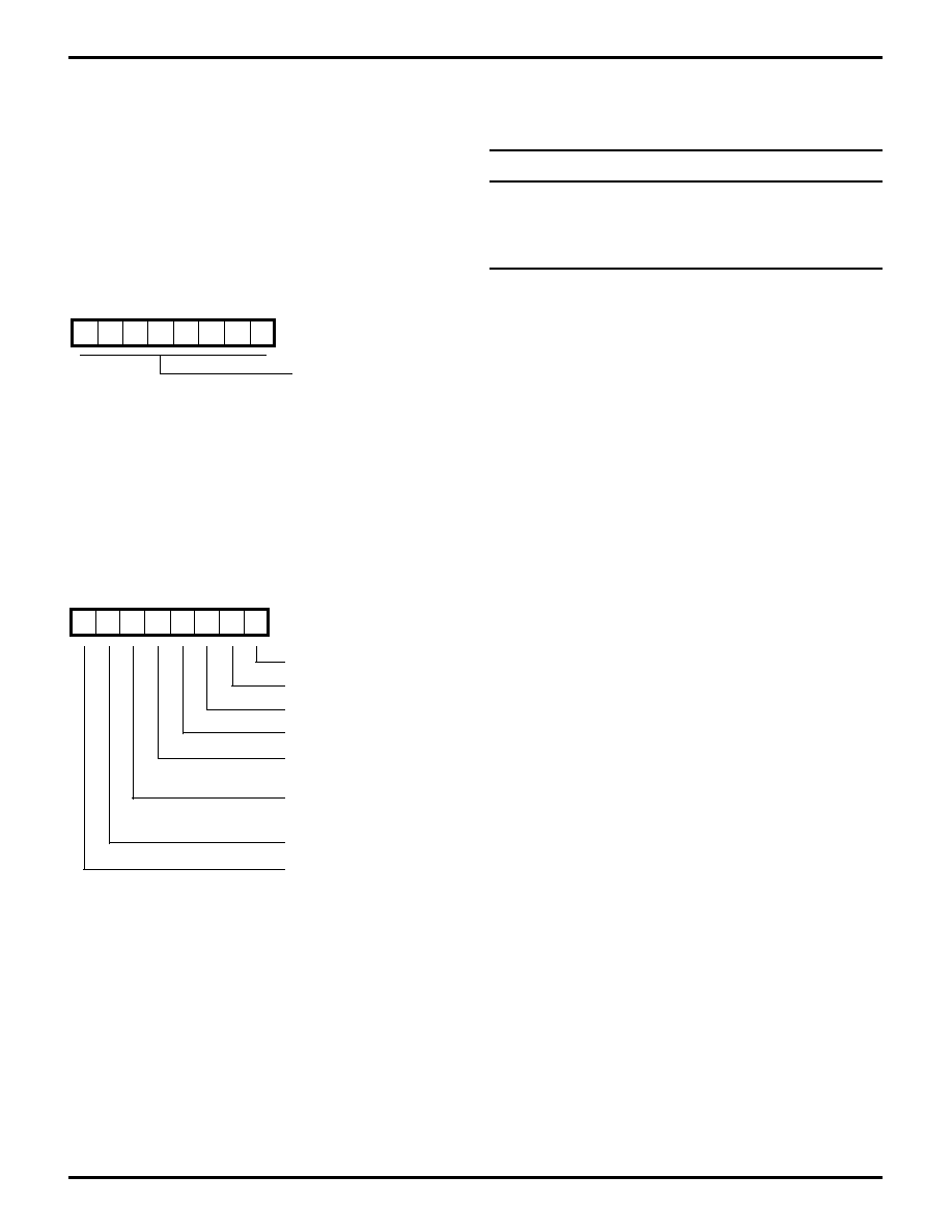
77
P R E L I M I N A R Y
Z80189/Z8L189
G
ENERAL
-P
URPOSE
E
MBEDDED
C
ONTROLLERS
DS971890301
Zilog
Transmit Holding Register
When the PC/XT/AT writes to the Transmitter Holding
Register, the Z80189 responds by setting the appropriate
bit in the IP register and by generating an interrupt to the
Z180 MPU if it is enabled. When the Z180 MPU reads this
register, the Transmitter Holding register empty flag is set
(if the transmitter timer is enabled, this bit is set after the
timer times out). In FIFO mode of operation, this address is
used to read (Z180) and write (PC) the Transmitter FIFO.
X
X
X
X
X
X
X
X
Transmitter Holding
Register
7
6
5
4
3
2
1
0
(PC Write Only, Address 00H, DLAB=0, R/W=Write)
(Z180 MPU Read Only, Address XXF0H)
Figure 90. Transmitter Holding Register
FIFO Control Register
Figure 91. FIFO Control Register
0
0
0
0
0
0
0
0
FIFO Enable
7
6
5
4
3
2
1
0
RCVR FIFO Reset
XMIT FIFO Reset
Reserved (Must be 0)
Reserved
(Tx Overrun, MPU Only)
Reserved
(FCR Write, MPU Only)
RCVR Trigger (LSB)
RCVR Trigger (MSB)
PC/XT/AT Write Only, PC Address 02h
Z180 MPU Read Only, MPU Address XXE9H
Bit 6 and Bit 7 RCVR trigger LSB and MSB bits
This 2-bit field determines the number of required bytes in
the receiver FIFO before an interrupt to the PC occurs.
b7
b6
Trigger Level, Number of Bytes
0
0
01
0
1
04
1
0
08
1
1
14
Bit 4 and Bit 5 Reserved
Note: From the MPU side, bit 4 and bit 5 flag two sources
of interrupts. Bit 5 is a FIFO interrupt, indicating that the
FCR had changed; bit 4 is a Tx overrun interrupt, indicating
transmit overrun. A read of the FCR from the MPU side will
clear a previously set bit 4 or bit 5.
Bit 3 Reserved
Reserved for future use.
Bit 2 XMIT FIFO Reset
Setting this bit to a 1 will cause the transmitter FIFO pointer
logic to be reset; any data in the FIFO will be lost. This bit
is self clearing; however, a shadow bit exists that is cleared
only when read by the Z180 MPU, allowing the MPU to
monitor a FIFO reset by the PC.
Bit 1 RCVR FIFO Reset
Setting this bit to a 1 will cause the receiver FIFO pointer
logic to be reset; any data in the FIFO will be lost. This bit
is self clearing; however, a shadow bit exists that is cleared
only when read by the Z180 MPU, allowing the MPU to
monitor a FIFO reset by the PC.
Bit 0 FIFO Enable
The PC writes this bit to logic 1 to put the 16550 MIMIC into
FIFO mode. This bit must be a 1 when writing to the other
bits in this register or they will not be programmed. When
this bit changes state, any data in the FIFO's or transmitter
holding and receiver buffer registers is lost and any pend-
ing interrupts are cleared.

78
P R E L I M I N A R Y
Z80189/Z8L189
G
ENERAL
-P
URPOSE
E
MBEDDED
C
ONTROLLERS
DS971890301
Zilog
Interrupt Identification Register
MIMIC Modification Register
0
0
0
0
0
0
0
0
Reserved - Program to Zero
D7 D6 D5 D4 D3 D2 D1 D0
16550/450 RCVR Overrun
Figure 92. MIMIC Modification Register
(Z189 MPU Write only, Address XXE9H)
Bit 7-2 Reserved.
Program to zero.
Bit 1 RCVR Overrun Modification
The actual 16450/16550 device allows the last position in
FIFO to be overwritten by MPU during receiver overrun
condition. When this bit is enabled (programmed to 1) the
last position in FIFO can be overwritten by Z180 during
receiver overrun. This feature is disabled by default. When
this modification is not enabled, the MIMIC will ignore any
write to RBR during an overrun condition.
Bit 0 Reserved
Program to zero.
0
0
0
0
0
0
0
0
0 if Interrupt Pending
7
6
5
4
3
2
1
0
Interrupt ID Bit (0)
Interrupt ID Bit (1)
Interrupt ID Bit (2)
Always 0
FIFO Enabled Flag
PC/XT/AT Read Only, PC Address 02H
Z180 MPU No Access
Figure 93. Interrupt Identification Register
Bit 7 and Bit 6 FIFO's enabled
These bits will read 1 if FIFO mode is enabled on the
MIMIC.
Bit 5 and Bit 4 Always read 0
Reserved bits.
Bits 3-1 Interrupt ID bits
This 3 bit field is used to determine the highest priority
interrupt pending. See Table 16 for the 3-bit field
descriptions.
Table 16. Interrupt Identification Field
b3
b2
b1
Priority
Interrupt Source
Inter. Reset Control
0
1
1
Highest
Overrun, Parity,
Read Line Stat. Reg.
Framing error or
Break detect bits
set by MPU.
0
1
0
2nd
Received Data
RCVR FIFO drops below
trigger level
trigger level.
1
1
0
2nd
Receiver Time-out
Read RCVR FIFO.
with data in
RCVR FIFO.
0
0
1
3rd
Transmitter
Writing to the
Holding Register
IIR or transmitter
Empty.
Holding Register.
0
0
0
4th
MODEM status:
Reading the MODEM
CTS,DSR,RI or
DCD.

79
P R E L I M I N A R Y
Z80189/Z8L189
G
ENERAL
-P
URPOSE
E
MBEDDED
C
ONTROLLERS
DS971890301
Zilog
Bit 0 Interrupt Pending
This bit is logic 0 and interrupt is pending. When the PC
accesses the IIR, the contents of the register and all
pending interrupts are frozen. Any new interrupts will be
recorded, but not acknowledged during the IIR access.
Line Status Register
0
0
0
1
0
0
0
0
Data Ready
7
6
5
4
3
2
1
0
Overrun Error
Parity Error
Framing Error
Break Interrupt (BI)
THRE
TEMT
Error in RCVR FIFO
PC/XT/AT Read Only, PC Address 05H
Z180 MPU Read/Write Bits 6,4,3,2 MPU Address XXF5H
Figure 94. Line Status Register
Bit 7 Error in RCVR FIFO
In 16450 mode, this bit will read logic 0. In 16550 mode, this
bit is set if at least one data byte is available in the FIFO with
one of its associated error bits set. This bit will clear when
there are no more errors (or break detects) in the FIFO.
Bit 6 Transmitter Empty
This bit must be set or reset by the MPU by a write to this
register bit. If Double Buffer Mode is enabled this bit is set
automatically by hardware whenever both THR buffer and
TSR is empty.
Bit 5 Transmitter Holding Register Empty, THRE
This bit is set to one when either the THR has been read
(emptied) by the MPU (16450 mode) or the XMIT FIFO is
empty (16550 mode). This bit is set to 0 when either the
THR or XMIT FIFO become non-empty. A shadow bit exists
so that the register bit setting to 1 is delayed by the
Transmitter Timer if enabled. The MPU when reading this
bit will not see the delay. Both shadow and register bits are
cleared when the PC writes to the THR of XMIT FIFO.
Note: The THRE bit is forced to 0 in the PC side to prevent
THR overruns when /HALT is asserted (Powerdown Mode)
and bit 3 (/INTO assertion on MIMIC access feature) is set.
When the MIMIC comes out of powerdown (/HALT
deasserted), the THRE bit resumes normal functionality.
Bit 2, 3, 4 Parity Error, Framing Error, Break Detect
These bits are written, indirectly, by the MPU as follows:
The bits are first written to shadow bit locations when the
MPU write accesses the LSR. When the next character is
written to the Receiver Buffer or RCVR FIFO, the data in the
shadow bits is then copied to the LSR (16450 mode) or
FIFO RAM (16550 mode). In FIFO mode, the bits become
available to the PC when the data byte associated with the
bits is next to be read (top of FIFO). In FIFO mode, with
successive reads of the receiver, the status bits will be set
if an error occurs on any byte. Once the MPU writes to the
Receiver Buffer or RCVR FIFO, the shadow bits are auto
cleared. The register bits are cleared upon the PC reading
the LSR. In FIFO mode, these bits will be set if any byte has
the respective error bit set while the PC reads multiple
characters from the FIFO.
Bit 1 Overrun Error
This bit is set if the Z180 MPU makes two writes to the
Receiver Buffer before the PC reads the data in the Buffer
(16450 mode) or with a full RCVR FIFO (16550) mode. No
data will be transferred to the RCVR FIFO under these
circumstances. This bit is reset when the PC reads the Line
Status Register.
Bit 0 Data Ready
This bit is set to 1 when received data is available, either in
the RCVR FIFO (16550 mode) or Receiver Buffer Register
(16450 mode). This bit is set immediately upon the MPU
writing data to the Receiver Buffer or FIFO if the Receiver
Timer is not enabled but is delayed by the timer interval if
the Receiver Timer is enabled. For MPU read access, a
shadow bit exists, so that the MPU does not see the delay
the PC does. Both bits are cleared to logic zero immedi-
ately upon reading all the data in either the Receiver Buffer
or FIFO.
Interrupt Enable Register
0
0
0
0
0
0
0
0
Bit 0 Received Data Available Int.
7
6
5
4
3
2
1
0
Bit 1 THRE Interrupt
Bit 2 Receiver Line Status Int.
Bit 3 Modem Status Interrupt
Bit 7,6,5,4 always 0
PC/XT/AT Read/Write, PC Address 01H
Z180 MPU Read Only, Z180 MPU Address XXF1H
Figure 95. Interrupt Enable Register
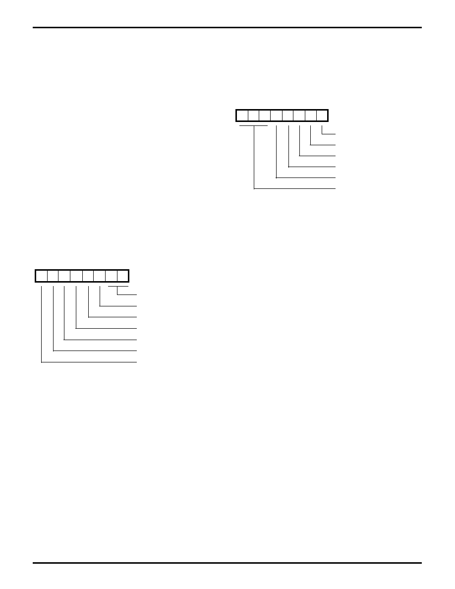
80
P R E L I M I N A R Y
Z80189/Z8L189
G
ENERAL
-P
URPOSE
E
MBEDDED
C
ONTROLLERS
DS971890301
Zilog
Bit 6-Bit 0
These bits do not affect the Z80189 directly; however, they
can be read by the Z180 MPU and the 16550 MIMIC
modes can be emulated by the Z180 MPU.
Modem Control Register
Interrupt Enable Register
(Continued)
Bits 7,6,5,4 Reserved
These bits will always read 0 (PC and MPU)
Bit 3 Modem Status IRQ
If bits 0,1,2 or 3 of the Modem Status Register are set and
this enable bit is a logic 1, then an interrupt to the PC is
generated.
Bit 2 Receiver Line Status IRQ
If bits 1,2,3 or 4 of the LSR are set and this enable bit is a
logic 1, then an interrupt to the PC is generated.
Bit 1 Transmitter Holding Register Empty IRQ
If bit 5 of the LSR is set and this enable bit is a logic 1, then
an interrupt to the PC is generated.
Bit 0 Received Data Available IRQ
If bit 0 of the LSR is set or a Receiver Timeout occurs and
this enable bit is a logic 1, then an interrupt to the PC is
generated.
Line Control Register
0
0
0
0
0
0
0
0
DALB
7
6
5
4
3
2
1
0
Set Break
Even Parity Sel.
Parity Enable
PC/XT/AT Read/Write, PC/XT/AT Address 3H
Z180 MPU Read Only, Z180 MU Address XXF3H
Number of Stop Bits
Word Length Sel.
Stick Parity
Figure 96. Line Control Register
Bit 7 Divisor Latch Access Bit (DALB)
This bit allows access to the divisor latch by the PC/XT/AT.
If this bit is set to a one, access to the Transmitter, Receiver
and Interrupt Enable Registers is disabled, and when an
access is made to address 0, the Divisor Latch Least
Significant byte is accessed and if an access is made to
address 1, the Divisor Latch Most Significant byte is
accessed.
0
0
0
0
0
0
0
0
7
6
5
4
3
2
1
0
Reserved
Loop
Out 2
PC/XT/AT Read/Write, PC/XT/AT Address 4H
Z180 MPU Read Only, Z180 MU Address XXF4H
Out 1
DTS
RTS
Figure 97. Modem Control Register
Bit 7-5 Reserved
Reserved for future use, always 0.
Bit 4 Loop
When this bit is set to a one then:
RI = Out 1
DCD = Out 2
DSR = DTR
CTS = RTS
Emulation of the loop back feature of the 16550 UART must
be done by the Z180 MPU except for the above conditions.
Bit 3 Out 2
This bit controls the state on the active HINTR pin if bits 2
and 1 of the MIMIC Master Control Register are a 10. Or
else it can be read by the Z180 MPU.
Bit 2-Bit 0
These bits have no direct control of the 16550 MIMIC
interface and the Z180 MPU must emulate the function if it
is to be implemented.

81
P R E L I M I N A R Y
Z80189/Z8L189
G
ENERAL
-P
URPOSE
E
MBEDDED
C
ONTROLLERS
DS971890301
Zilog
Modem Status Register
0
0
0
0
0
0
0
0
DCTS
7
6
5
4
3
2
1
0
DDSR
TERI
DDCD
CTS
DSR
RI
DCD
PC/XT/AT Read Only, PC/XT/AT Address 6H
Z180 MPU Read/Write Bits 7-4, Z180 MPU Address XXF6H
Figure 98. Modem Status Register
Bit 7 Data Carrier Detect
This bit must be written by the Z180 MPU.
Bit 6 Ring Indicator
This bit must be written by the Z180 MPU.
Bit 5 Data Set Ready
This bit must be written by the Z180 MPU.
Bit 4 Clear to Send
This bit must be written by the Z180 MPU.
Bit 3 Delta Data Carrier Detect
This bit is set to a one whenever the Data Carrier Detect bit
changes state. This bit is reset when the PC/XT/AT reads
the Modem Status Register.
Bit 2 Trailing Edge Ring Indicator
This bit is set to a one on the falling edge of the Ring
Indicator bit. This bit is reset when the PC/XT/AT reads the
Modem Status Register.
Bit 1 Delta Data Set Ready
This bit is set to a one whenever the Data Set Ready bit
changes state. This bit is reset when the PC/XT/AT reads
the Modem Status Register.
Bit 0 Delta Clear To Send
This bit is set to a one whenever the Clear To Send bit
changes state. This bit is reset when the PC/XT/AT reads
the Modem Status Register.
Scratch Register
Figure 100. Divisor Latch (LS)
Bit 7-0 Divisor Latch Most Significant (MS)
This register contains the low order byte of the Baud rate
divisor. Writing to this register with the PC/XT/AT will
generate an interrupt to the Z180 MPU. It can then read the
Baud rate divisor and set up the application.
Divisor Latch (MS)
Figure 101. Divisor Latch (MS)
Bit 7-0 Divisor Latch Most Significant (MS)
This register contains the high order byte of the Baud rate
divisor. Writing to this register with the PC/XT/AT will
generate an interrupt to the Z180 MPU. It can then read the
Baud rate divisor and set up application.
X
X
X
X
X
X
X
X
Scratch Register
7
6
5
4
3
2
1
0
PC/XT/AT Read/Write, PC/XT/AT Address 07H
Z180 MPU Read Only, Z180 MPU Address XXF7H
Figure 99. Scratch Register
Bits 7-0 Scratch Register
This register is used by the PC/XT/AT programmer for
temporary data storage. The Z180 MPU is able to read this
register. If the PC/XT/AT writes to this register, no interrupt
to the Z180 MPU is generated.
Divisor Latch (LS)
X
X
X
X
X
X
X
X
Divisor Latch (LS)
7
6
5
4
3
2
1
0
PC/XT/AT Read/Write, PC/XT/AT Address 00H and DLAB = 1
Z180 MPU Read Only, Z180 MPU Address XXF8H
X
X
X
X
X
X
X
X
Divisor Latch (MS)
7
6
5
4
3
2
1
0
PC/XT/AT Read/Write, PC/XT/AT Address 01H and DLAB = 1
Z180 MPU Read Only, Z180 MPU Address XXF9H

82
P R E L I M I N A R Y
Z80189/Z8L189
G
ENERAL
-P
URPOSE
E
MBEDDED
C
ONTROLLERS
DS971890301
Zilog
PC DMA Mailbox
General Description
The concept behind the PC DMA Mailbox Registers is to
provide a path for the PC DMA data transfer separate from
the MIMIC COM Port. Commands and data flow over the
COM Port, while the DMA path is reserved for other
purposes. The PC DMA Mailbox Register functionality will
require control registers which will allow PC DMA data
transfer between the PC memory and for example, a
modem speaker/microphone codec. Note that the transfer
will be driven by the PC Host DMAs. This feature only
allows for the handshaking and data path for the PC Host
DMAs.
The host (PC) DMA channels will use the following four
Z189 pins for the PC DMA Mailbox feature. Each pair of
pins are individually selectable:
HDRQ0
Host DMA request 0, Z189 output,
active high, high-Z control
/HDACK0
Host DMA acknowledge 0, Z189 input,
active low
HDRQ1
Host DMA request 1, Z189 output,
active high, high-z control
/HDACK1
Host DMA acknowledge 1, Z189 input,
active low
The pins labeled as HDRQ0 and HDRQ1 are asserted by
the Z180 to signal the PC HOST of a DMA request. The pins
labelled /HDACK0 and /HDACK1 are asserted by the PC
to signal a PC DMA access. Dual request/acknowledge
pairs are provided to interface with two PC DMA channels.
The PC Mailbox channels are independent and can be
used simultaneously or individually for jumperless DMA
channel selection.
PC DMA MAILBOX BIT FUNCTIONS
HDREQ. Host DMA request bit, default value = 0
Two bits will serve to request a PC HOST DMA access.
When this bit is set and the Host DMA channel is enabled
(HDMAE=1), the corresponding HDRQ pin will be as-
serted high. Z180 software sets this bit (OUT0 instruction)
to request a DMA transfer, and Z189 hardware clears the
bit when the byte transfer is complete. Z180 software can
also clear the bit. The Z180 will be able to read the bit (IN0
instruction) to indicate that the transfer has occurred.
I/O address of XXD2h (HMC register) contains a request
bit for each DMA channel (bit 4 and bit 5 of the HMC
register). Write enable bits are provided to simplify code
(read-modify-write cycles not required).
HDMAE Host DMA enable default=0, HDRQ is tri-stated
Two bits will serve to enable the dual DMA channels
request/acknowledge pairs. When the HDMAE1 bit is set,
the output will become fully driven, otherwise (HDMAE1 bit
is reset) the HDRQ1 will be tri-stated. When the HDMAE0
bit is set the HDRQ0 output will become fully driven,
otherwise, the HDRQ0 output will be tri-stated.
I/O address XXD2h is assigned the HMC register. Bits 0
and 1 of the HMC register are respectively assigned
HDMAE0 and HDMAE1.

83
P R E L I M I N A R Y
Z80189/Z8L189
G
ENERAL
-P
URPOSE
E
MBEDDED
C
ONTROLLERS
DS971890301
Zilog
3.
Z189 hardware forces HDRQ inactive low on the
leading (falling) edge of /HWR during the /HDACK
cycle. Note that the HDREQ register bit is not to be
cleared yet, since the DMA cycle has not yet com-
pleted.
4.
The PC places valid data on the ISA bus (HD[0:7] and
asserts /HWR low.
5.
Z189 hardware latches data into the HDMAT register
on the trailing (rising) edge of /HWR while /HDACK is
still active low. On this same edge, hardware clears the
HDREQ register bit.
6.
Z180 software polls the HDREQ bit until it's 0, and then
can input the data byte from HDMAT. The polling of the
HDREQ bit is used to indicate when the PC DMA Write
has been completed. The PC software program should
program its DMA controller to stop DMA at the end of
valid data or when commanded by the application.
When the Z180 software sets HDREQ, but doesn't see
the HDREQ bit automatically cleared within a reason-
able time (because /HDACK remains inactive high),
then software can stop the PC DMA write by resetting
the HDREQ bit.
7.
Messages on the COM Port confirm that the PC DMA
write operation is complete. Z180 software clears
HDREQ, then clears HDMAE to disable host DMA.
PC DMA Read
PC DMA Read is almost the same as a PC DMA Write, but
the data flows the other direction through the HDMAR
register.
Through commands exchanged over the MIMIC COM
Port, PC software and the Z180 agree to configure DMA for
a PC DMA Read, in which data flows from, for example, a
modem's microphone codec to PC memory. The PC sets
up its 8237 DMA controller in auto-initialize mode to assure
that there is always buffer space available whenever the
modem makes a DMA request. The Z180 clears HDREQ
and sets HDMAE, forcing HDRQ low.
The PC DMA Read proceeds as follows:
1.
Z180 software outputs the data byte to HDMAR, where
it is latched.
2.
Z180 software writes a 1 to the HDREQ bit, causing the
HDRQ pin to go active high.
PC MAILBOX DATA REGISTERS
HDMAT0
Host DMA Transmit Register 0,
Z180 Read Only, PC Write Only
HDMAT1
Host DMA Transmit Register 1,
Z180 Read Only, PC Write Only
HDMAR0
Host DMA Receive Register 0,
Z180 Write Only, PC Read Only
HDMAR1
Host DMA Receive Register 1,
Z180 Write Only, PC Read Only
There are four separate 8-bit mailbox registers available
for DMA data. The I/O address for the mailbox registers will
be XXDOH for Mailbox 0 and XXD1H for Mailbox 1. Note
that there are separate registers for read and write access.
The mailbox register can latch data from the host data bus
HD[0:7] and is readable by the Z180 using IN0 a, (DOH) or
IN0 a, (D1H). Data can be written into the mailbox registers
using the OUT0 (DOH), a or OUT0 (D1H), a and can output
its contents onto HD [0:7} during a PC HOST DMA access.
Note: The following is a description of other Z189 signals
relevant in a PC DMA Mailbox access.
≠
The /HDDIS signal will go low during a PC DMA Read
access (selected /HDACK and /HRD going low).
≠
The /HCS pin will not asserted low during a PC DMA
Mailbox access (/HDACK active) if the HDRQ/HDACK
channel is enabled.
PC DMA Write
Through commands exchanged over the MIMIC COM
Port, PC software and the Z180 agree to configure DMA for
a PC DMA write, in which data flows from PC memory to,
for example, a modem's speaker codec. The PC sets up its
8237 DMA controller in auto-initialize mode to assure that
data is always available whenever the modem makes a
DMA request. The Z180 clears HDREQ and sets HDMAE,
forcing HDRQ low.
The PC DMA Write proceeds as follows:
1.
Z180 software writes a 1 to the HDREQ bit, causing the
HDRQ pin to go active High.
2.
The rising edge of HDRQ causes the 8237 DMA
controller to begin a memory-read, I/O-write DMA bus
cycle on the ISA bus at the end of the current PC bus
cycle. The PC asserts /HDACK low to acknowledge
the DMA request.

84
P R E L I M I N A R Y
Z80189/Z8L189
G
ENERAL
-P
URPOSE
E
MBEDDED
C
ONTROLLERS
DS971890301
Zilog
PC MAILBOX DATA REGISTERS
(Continued)
3.
The rising edge of HDRQ causes the 8237 DMA
controller to begin an I/O-read, memory-write DMA
bus cycle on the ISA bus at the end of the current PC
bus cycle. The PC asserts /HDACK low to acknowl-
edge the DMA request.
4.
Z189 hardware forces HDRQ inactive low on the
leading (falling) edge of /HRD during the /HDACK
cycle. Note that the HDREQ register is not to be
cleared yet, since the DMA cycle has not completed.
5.
The PC asserts /HRD low while /HDACK is still active
low, causing Z189 hardware to enable the latched
HDMAR byte onto HD[0:7].
6.
While Z189 hardware holds valid data on the ISA bus,
the PC does its memory-write half of the DMA cycle.
On the trailing (rising) edge of /HRD, Z189 hardware
disables the output of the HDMAR register, putting
HD[0:7] in high impedance state. On this same edge,
hardware clears the HDREQ register bit. Note: /HDDIS
will go low while the HDMAR register is accessed on
the ISA bus.
7.
Z180 software polls the HDREQ bit until it's 0, then
continues with step 0 for the next byte.
PC DMA Read will not be stopped as with the case for PC
DMA Write if the HDREQ handshake is not met. If software
fails to see HDREQ reset soon after making the DMA
request (because /HDACK remains inactive high), Z180
software should clear HDREQ and HDMAE and configure
the data pump to stop the PC DMA Read.
Logic Equations for PC DMA Read/Write
This section summarizes the significant events for PC DMA
Read/Write that was explained in the previous sections.
This section can be used as a quick check of the circuit
implementation.
Set HDREQ bit:
I/O write 1 to HDREQ bit in HMC register.
Clear HDREQ bit:
Reset
OR I/O write 0 to HDREQ bit in HMC register
OR (Rising edge of (/HRD and /HWR) while /HDACK=0)
Drive HDRQ pin active high:
HDREQ bit = 1 while HDMAE=1
Drive HDRQ pin inactive low:
Reset
OR /HDACK=0
OR HDREQ bit = 0
Latch PC DMA Write data to HDMAT register:
HDMAE=1
AND /HDACK=0
AND /HWR=0
Drive PC DMA Read data from HDMAR register:
HDMAE=1
AND /HDACK=0
AND /HRD=0
Selectable DMA Channels
The Z189 features jumperless selection of PC DMA chan-
nels. On the 8-bit PC/XT bus, DMA channels 0 and 3 are
generally available, therefore reference designs may con-
nect to those. 2 HDREQ bits and 2 HDMAE Enable bits are
used to enable which PC DMA Channel is to be imple-
mented. In addition, there are two additional bits which
allow for the multiplexing of PC DMA Mailbox functions with
Bus Mastering and Z180 peripheral functions.
PC DMA Mailbox Pin Designations
The four request/acknowledge pins will be designated as
follows, and are assigned the following QFP pins as shown
below:
HDRQ, pin 50, output (mux with RTS0)
/HDACK0, pin 43, input (mux with CKA0 and /DREQ0)
HDRQ1, pin 97, output (mux with /BUSACK)
/HDACK1, pin 98, input (mux with /BUSREQ)

85
P R E L I M I N A R Y
Z80189/Z8L189
G
ENERAL
-P
URPOSE
E
MBEDDED
C
ONTROLLERS
DS971890301
Zilog
PC MAILBOX DATA REGISTERS
(Continued)
1
1
0
0
0
0
0
0
7
6
5
4
3
2
1
0
0 = HDRQ0 Tri-State
1 = HDMA Enable
0 = HDRQ1 Tri-State
1 = HDMA Enable
HDRQ /HDACK0,
CKA0//DREQ0, /RTS0
0 = HDRQ0, /HDACK0 Select
1 = /RTS0, CKA0//DREQ0 Select
HDRQ1, /HDACK1,
/BUSACK, /BUSREQ
0 = HDRQ1, /HDACK1 Select
1 = /BUSACK, /BUSREQ Select
HDREQ0 (DMA request 0)
HDREQ1 (DMA request 1)
Revision Data Avail
Write Enable HDREQ0
Revision Data Avail
Write Enable HDREQ1
Figure 102. Host DMA Mailbox
Control Register, HMC
(Z180 MPU Read/Write Address XXD2H)
Bits 7 Write Enable HDREQ1 (Write only)
Revision Data Available (Read only)
Set this bit whenever setting/resetting the HDREQ1 bit.
When this bit is written with 1, bit 5 will be written into the
HDREQ bit and bits 0-3 are ignored. When this bit is written
with zero, bits 0-3 can be written and bit 5 is ignored. Note
that this bit does not change the write access to bits 4 and
6. The Write Enable is not latched and must be set for each
HDREQ1 write.
When bit 7 is read it is set upon powerup and becomes
reset during the 1st read of the HDMAT1 register.
Bits 6 Write Enable HDREQ0 (Write only)
Set this bit whenever setting/resetting the HDREQ0 bit.
When this bit is written with 1, bit 4 will be written into the
HDREQ0 bit and bits 0-3 are ignored. When this bit is
written with zero, bits 0-3 can be written and bit 4 is
ignored. Note that this bit does not change the write
access to bits 5 and 7. The Write enable is not latched and
must be set for each HDREQ0 write.
When bit 6 is read, it indicates the availability of the revision
data in the Host DMA transmit register (HDMAT0). When
the revision data is read by the Z180 CPU, this bit will
become reset and the revision data will no longer be
available in the HDMAT0 register.
Bit 5 HDREQ1 Bit
When Mailbox 1 is multiplexed and enabled (HDMAE1=1),
setting this bit will cause the HDRQ1 pin to go active high,
which puts out a request to the PC for a DMA transfer. Z189
hardware clears this bit when byte transfer is complete.
This bit is disabled upon reset. This bit can also be reset to
force the HDRQ1 pin to inactive low. Note that Bit 7 must
be set to modify HDREQ1.
Bit 4 HDREQ0 Bit
When Mailbox 0 is multiplexed and enabled (HDMAE0=1),
setting this bit will cause the HDRQ0 pin to go active high,
which puts out a request to the PC for a DMA transfer. Z189
hardware clears this bit when byte transfer is complete.
This bit is disabled upon reset. This bit can also be reset to
force the HDRQ0 pin to inactive low. Note that Bit 6 must
be set to modify HDREQ0.
Bit 3 HDRQ1/HDACK1, /BUSACK /BUSREQ
This bit selects the multiplexing that will occur between the
HDRQ1//BUSACK and the /HDACK1/BUSREQ pins. If this
bit is set to 0, the HDRQ1 and /HDACK1 functions are
enabled for this pin. Otherwise, if this bit is set to 1, the
/BUSACK and /BUSREQ functions are enabled for this pin.
This bit is reset to 0.
Bit 2 HDRQ/HDACK0, /RTS0 CKA0//DREQ0
This bit selects the multiplexing that will occur between the
HDRQ0//RTS0 and the /HDACK/CKA0//DREQ0 pins. If this
bit is set to 0, the HDRQ and /HDACK0 functions are
enabled for this pin. Otherwise, if this bit is set to 1, the
CKA0//DREQ0 and /RTS0 functions are enabled for this
pin. This bit is reset to 0.
Bit 1 HDMAE1 bit
When this bit is set to 1, it allows Mailbox 1 to request a PC
DMA cycle given that the Mailbox 1 pins are multiplexed
(bit 4=1). When this bit is cleared to 0, the HDREQ1 is tri-
stated if Mailbox 1 pins are multiplexed. When this bit is
cleared, the HDMAT1 can be used to store HOST OUTPUT
MAILBOX DATA.
Bit 0 HDMAE0 bit
When this bit is set to 1, it allows Mailbox 0 to request a PC
DMA cycle given that the Mailbox 0 pins are multiplexed
(bit 4=1). When this bit is cleared to 0, the HDREQ0 is tri-
stated if Mailbox 0 pins are multiplexed.
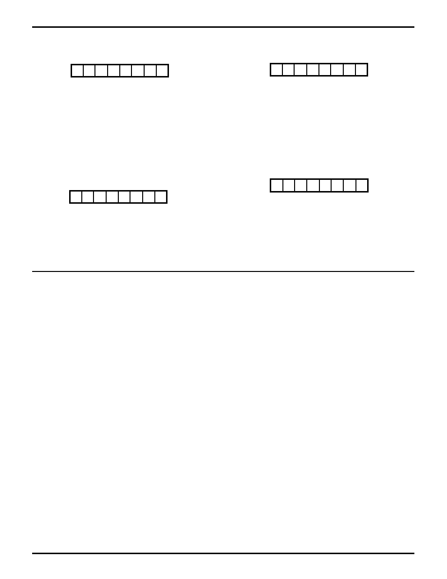
86
P R E L I M I N A R Y
Z80189/Z8L189
G
ENERAL
-P
URPOSE
E
MBEDDED
C
ONTROLLERS
DS971890301
Zilog
PC DMA MAILBOX DATA REGISTERS
1
0
0
1
0
0
0
1
7
6
5
4
3
2
1
0
Figure 103. Host DMA Transmit Register, HDMAT0
(Z180 MPU Read Only Address XXD0H)
(PC Write Only)
Note:
91hex is defaulted into this register to indicate
revision (9 for Z189 and 1 for 1st revision). Once the
revision data is read by the Z180 CPU, bit 6 of the HMC
register (Revision Data Avail bit) will be read as zero.
0
0
0
0
0
0
0
0
7
6
5
4
3
2
1
0
Figure 105. Host DMA Transmit Register, HDMAT1
(Z180 MPU Read Only Address XXD1H)
(PC Write Only)
HDMAT1 can also be used as a HOST OUTPUT MAILBOX
DATA REGISTER. Refer to Host Output Mailbox function
for details.
0
0
0
0
0
0
0
0
7
6
5
4
3
2
1
0
Figure 106. Host DMA Receive Register, HDMAR1
(Z180 MPU Write Only Address XXD1H)
(PC Read Only)
HOST INPUT/OUTPUT MAILBOX ENHANCEMENTS
The purpose of Host I/O Mailbox is to provide an additional
data path between PC HOST and Z80189 in a Modem
Control Application. This is required in order to accommo-
date transfer of data other than data (flows through COM
Port) or audio (flows through PC DMA MAILBOX). An
example implementation of this feature is described
below:
≠
PC HOST controlled COM Port selection. In a Psuedo
"Plug & Play" environment, the PC BIOS will assign a
modem to a COM Port address upon powerup. There-
fore, the Modem will need to "listen" to the PC bus for
BIOS calls that query the existence of a modem card.
0
0
0
0
0
0
0
0
7
6
5
4
3
2
1
0
Figure 104. Host DMA Receive Register, HDMAR0
(Z180 MPU Write Only Address XXD0H)
(PC Read Only)
The modem will then need to reply and output informa-
tion on its capabilities and requirements. The PC BIOS
will then assign the Modem to a COM Port and interrupt
such that there are no resource conflicts.
In order to facilitate the feature listed above, a communica-
tion path needs to be available between a PC BIOS and
Modem PRIOR to the selection of COM Port, DMA, or IRQ
selection.
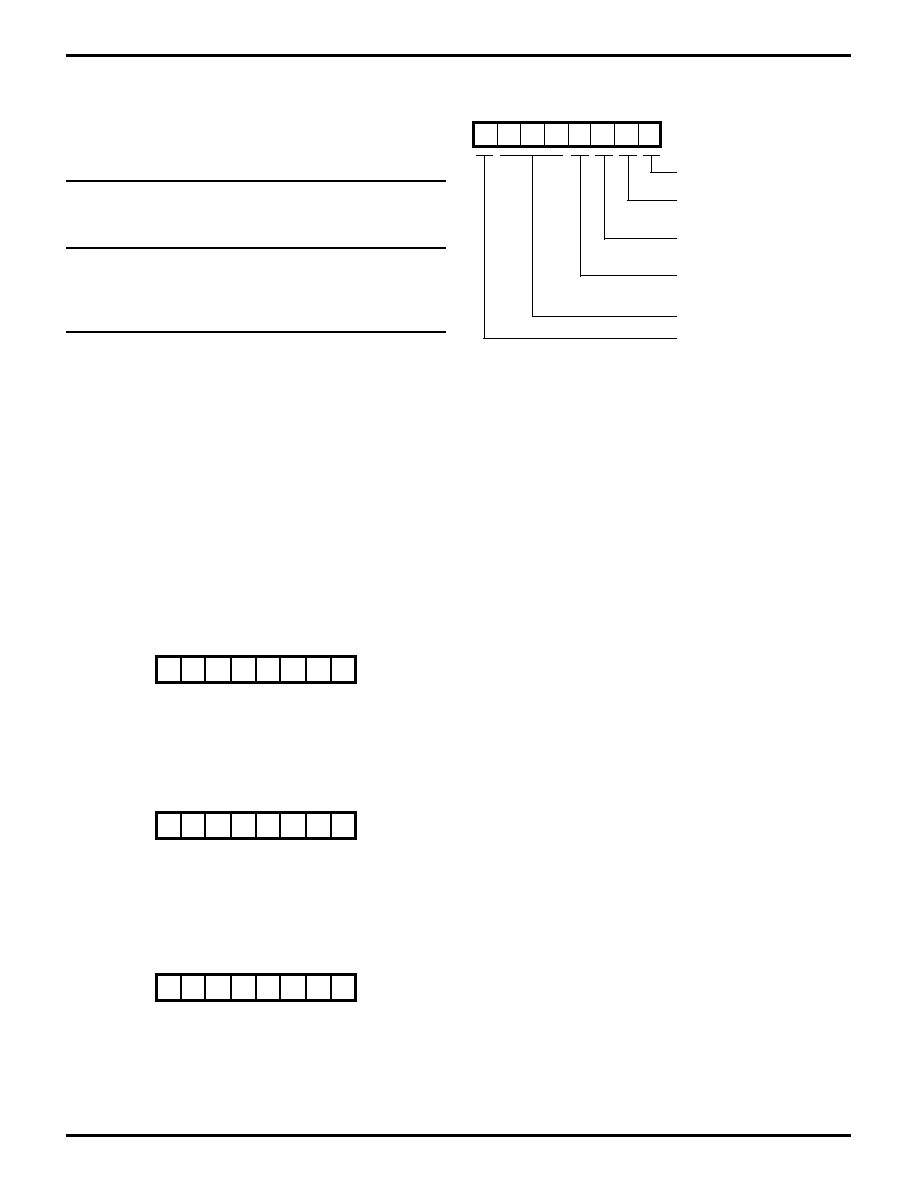
87
P R E L I M I N A R Y
Z80189/Z8L189
G
ENERAL
-P
URPOSE
E
MBEDDED
C
ONTROLLERS
DS971890301
Zilog
Enhancement Detail
PC HOST Address Selection. There are a total of 4 regis-
ters addresses that are accessible by the PC HOST. They
are as follows:
Address
HA9-HA2 programmable
Function
HA1
HA0
Host Output Register 0
0
0
Host Output/Input Register 1
0
1
Host I/O Status Register
1
0
*Host Output to HDMAT1 Register
1
1
The HA9-HA2 is programmable by writing the contents into
Port A Data Register. The PC HOST access will occur
during a PC HOST input/output cycle at the programmed
address range (/HRD or /HWR=0, HAEN=0,
PA[9:2]=PADATA[7:0]).
NOTE: PADATA SHOULD BE
WRITTEN WITH THE ADDRESS RANGE PRIOR TO
ENABLING THIS FEATURE.
* If the Host DMA Mailbox 1 function is disabled (bit 1 of
HMC register is zero), a Host write in the programmed
Mailbox range with HA1,0=1,1, will cause the host data to
be latched into the HDMAT1 register. This can be used as
an auxiliary host output register. Note that a host read from
this address is invalid.
0
0
0
0
0
0
0
0
7
6
5
4
3
2
1
0
Figure 107. Host Output Register 0 (HOR0)
(180 MPU Read Only Address XXD3H)
(PC Host Read/Write HA9-2 (PADATA) + 00b)
Figure 108. Host Output Register 1 (HOR1)
(180 MPU Read Only Address XXD4H)
(PC Host Write Only HA9-2 (PADATA) +01b)
0
0
0
0
0
0
0
0
7
6
5
4
3
2
1
0
Host Output Register 1
Data Available
Host Input Register 1
Data Available
Auxilliary Bits
Host I/O Mailbox Enable
Unlock Bit
Host Output Register 0
Data Available
Figure 110. Host I/O Status Register (HIOS)
(180 MPU Read/Write Address xxD5H)
(PC Host Read Only HA9-HA2 (PADATA) + 10b)
Bit 7.
Host I/O Mailbox Enable. The Z180 must write a logic
one to this bit to enable the Host I/O Mailbox. When this bit
is at zero (default), Host accesses are disabled. This bit is
only writable by the Z180, but is readable by both Z180 and
PC Host. When this bit is zero, registers D3, D4 and D5
cannot be read or written except for a write to the enable
bit in register D5 bit 7. Also, when this bit is zero the Host
side is not accessible. Once this bit is set, all registers
become visible to the Z180 and the Host.
Note:
The PADATA should be programmed with HA9:HA2
address range prior to setting this bit. This bit should be
programmed as zero when the COM Decode Mux (CDR bit
0) is disabled.
Bits 6-4.
Auxiliary bits. these bits can be written by the
Z180 and can be read by both the PC HOST and the Z180.
Note that the PC HOST cannot write to these bits. The
Auxillary Bits are zero by default and have no function other
than to serve as scratch bits for the HOST I/O Mailbox.
Bit 3.
Host Input Register 1 Data Available. This bit be-
comes set when the Z180 writes to the Host Input Register
1. A PC Host read of the Host Input Register 1 will cause
this bit to clear. This bit cannot be set unless the Host I/O
Mailbox enable bit is set.
Bit 1.
Host Output Register 0 Data Available. This bit
becomes set when the PC Host writes to the Host Output
Register 0. A Z180 read of the Host Output Register 0 will
cause this bit to clear. This bit cannot be set unless the Host
I/O Mailbox enable bit is set.
0
0
0
0
0
0
0
0
7
6
5
4
3
2
1
0
0
0
0
0
0
0
0
0
7
6
5
4
3
2
1
0
Figure 109. Host Input Register 1 (HIR1)
(180 MPU Write Only Address XXD4H)
(PC Host Read Only HA9-2 (PADATA) + 01b)

88
P R E L I M I N A R Y
Z80189/Z8L189
G
ENERAL
-P
URPOSE
E
MBEDDED
C
ONTROLLERS
DS971890301
Zilog
HOST INPUT/OUTPUT MAILBOX ENHANCEMENTS
(Continued)
If COM Port decode is disabled and COM Port decode
mux is enabled (default), COM Decode Pins HA9-HA3,
HAEN are ignored inputs. If HC1 is forced low the MIMIC
Data latch will be forced open. Therefore, care should be
taken that the HC1//HCS pin is NEVER connected directly
to logic high or low, when COM Port Decode is disabled.
/HCS pin can also be programmed as an output for debug
purposes. When the /HCS Force bit (Bit 7 in the COM Port
Decode Register) is enabled, the /HCS pin will be asserted
low whenever the MIMIC is being accessed by the PC host.
This feature is only available when the COM Port Decode
is enabled.
A dual HINTR option will provide two MIMIC Interrupt
requests to the HOST. HINTR1 will be asserted during a
MIMIC interrupt request when COM Decode is configured
for COM 1 & 3. HINTR2 will be asserted during a MIMIC
interrupt request when COM Decode is configured for
COM 2 & 4. The unasserted HINTR line will be tri-stated.
Note that during initialization, the COM Decode Regis-
ter must be written to before the System Configuration
Register.
Single Baud Rate Generator
A Baud Rate Generator is included to provide emulation
timing for the MIMIC device. This BRG is very similar to
ESCC BRG in functionality. There are 2x8 bit registers to
program the clock divider. The input to the BRG is the PHI
clock output of the S180 core.
The time constant required for a specific bit rate is as
follows:
Time constant (decimal) = (PHI freq. / (2*baud rate))-2
This formula is exactly the same as used in the ESCC.
The output of the BRG is directly connected to MIMIC
emulation counter input.
Bit 0.
Unlock Bit. When the Host I/O Mailbox is enabled, a
PC Host Write to Address 0FBHex will cause this bit to set.
A PC host write to address 0F9hex will cause this bit to
reset. The data written to these registers will NOT be
stored. A read access or access with HAEN=1 will NOT
cause this bit to toggle. Note that this bit has no function
other than a status bit (there is no locking or unlocking
caused by the state of this bit). The state of the unlock bit
is not controlled by the Host I/O Mailbox bit. Any I/O write
to FB will set the bit and a write to F9 will clear it regardless
of the state of the Host I/O Mailbox enable bit. Note that the
data written to 0FBhex or 0F9hex will not be stored by the
Z189.
I/O Chip Select w/Prog. Range
The Z80187 has two I/O Chip Selects labelled
/IOCS1 and /IOCS2. The /IOCS1 will have same function-
ality as the Z80182's /IOCS pin (multiplexed with IEO and
active during I/O accesses between ranges XX80H to
XXBFH). The IOCS pins will be asserted if /IORQ is active,
/M1 is inactive, and address compare is within range.
The Z80189 also has a secondary IOCS labeled
/IOCS2. This pin will be active for I/O accesses in the range
of XXC0H - XXC7H or XXC8H-XXCFH. The /IOCS2 pin will
be multiplexed over the E pin when enabled.
COM Port Decode
COM Port decode allows MIMIC to be selected when PC
address HA9-HA3 specifies a selected COM port address
range by HC pins 1 and 2 (selects COM Port address 1-4).
HC1 and HC2 can be read in software and program an
appropriate comport range for the decode circuitry. HC1
and HC2 can also be used for general input purposes. The
status of these pins can also be read when the COM
Decode Mux is disabled.

89
P R E L I M I N A R Y
Z80189/Z8L189
G
ENERAL
-P
URPOSE
E
MBEDDED
C
ONTROLLERS
DS971890301
Zilog
Baud Rate Generator Register
The following registers are used to store BRG constant.
The timer is enabled after setting bit 0 of IOBRG register.
Design is such that on-the-fly modification of registers do
not cause irregular BRG output.
Lower Byte of
Time Constant
7
6
5
4
3
2
1
0
1
1
1
1
1
1
1
1
IOBRG Register
The following register handles the IOCS feature and MIMIC
BRG. IOBRG-IOCS & BRG enable (Address XXD6H)
Default 04 hex.
0
0
0
0
0
1
0
0
BRG Enable
7
6
5
4
3
2
1
0
/IOCS2 Range
1 = I/O Access between
xxC0h-xxC7
0 = I/O Access between
xxC8h-xxCF
/IOCS2 Enable
/INTO Assertion of
MIMIC Access
Reserved as 0
Figure 113. IOBRG-IOCS and BRG Enable
(Address XXD6H)
Bits 4-7 Reserved
Bit 3
/INT0 assertion on MIMIC access. When this bit
R/W
is enabled, and the /HALT is active (power-down)
any HOST access to the MIMIC will cause a low
edge. Since this interrupt source has no vector,
/INT0 MODE 1 must be used when enabling this
mode. This is disabled on power-up. /INT0 asser-
tion is released when /HALT is deasserted.
Note:
The THRE bit is forced to 0 on the PC side to prevent
THR overrun during powerdown modes when this feature
is enabled. When the MIMIC comes out of power-down,
THRE resumes normal functionality.
Bit 2
/IOCS2 enable
When set, IOCS2 is muxed over E pin. This is
enabled on reset.
Bit 1
/IOCS2 range.
R/W
When set, IOCS2 is active during I/O accesses
between XXC0H-XXC7H.
When reset, IOCS2 is active during I/O accesses
between XXC8H-XXCFH. This is disabled on
power-up.
Bit 0
BRG enable. When set,
R/W
the MIMIC BRG begins counting down to gener-
ate a programmed square wave to the MIMIC
emulation timers. This is disabled on power-up.
Note:
When waking from Standby Mode using a PC-THR
write, the THRE bit will not reset until clock is stabilized.
This may cause a THR overrun. Therefore, data integrity
cannot be guaranteed. Care should be taken so that
standby mode is only used when data integrity is not
essential.
Figure 111. BRGL Baud Rate Generator Low
(Address XXE0H) Default 00 Hex
Upper Byte of
Time Constant
7
6
5
4
3
2
1
0
1
1
1
1
1
1
1
1
Figure 112. BRGH Baud Rate Generator High
(Address XXE9H) Default 00 Hex

90
P R E L I M I N A R Y
Z80189/Z8L189
G
ENERAL
-P
URPOSE
E
MBEDDED
C
ONTROLLERS
DS971890301
Zilog
HOST INPUT/OUTPUT MAILBOX ENHANCEMENTS
(Continued)
0
0
0
0
0
0
0
1
COM Port Decode MUX
7
6
5
4
3
2
1
0
State of HC1 (Read Only)
COM Port Decode Selection
Bit 4 3
0 0 COM 1 (3F8-3FF) Default
Reserved as 0
0 1 COM 2 (2F8-2FF)
1 0 COM 3 (3E8-3EF)
1 1 COM 4 (2E8-2EF)
COM Port Decode Enable
Dual HINTR
State of HC2
decoder during a PC-DMA cycle. This circuitry is
not used when COM Port Decode (bit 5) is dis-
abled.
HA2-HA0 are used to select between internal
MIMIC registers.
Bit 5
COM Port Decode enable. When this bit
R/W
is set, HA3-HA9 inputs are used for COM Port
Decoder. The MIMIC will be accessible given
that the address inputs HA3-HA9 are within the
range programmed by bits 3 & 4 when HAEN
is active low.
Please refer to MULTIPLEXING section for de-
tails on pin HA3-HA9 muxing. This is disabled
on reset. When disabled, the COM Port De-
code inputs are still treated as inputs, but have
no affect on MIMIC operation.
Bit 6
Dual HINTR. When this bit is set, the
R/W
HINTR2 output will be asserted for MIMIC
interrupt requests when configured for COM 2
& 4. HINTR1 output will be asserted for MIMIC
interrupt requests when configured for COM 1
& 3. When disabled, HINTR2 is always inactive
(tri-stated) while HINTR1 is active for all MIMIC
interrupt requests. This is disabled on reset
(HINTR2 is tri-state on power-up).
Note that the unselected HINTR line will be tri-
stated while the active HINTR line will be driven
as per the MIMIC Master Control Register
Bit 7
/HCS Force Bit. When Bit 0 and Bit 5 of this
register is set to 1 (COM Decode Mux and
Logic Enabled), it forces the /HCS signal to be
exported out of the /HCS/HC1 pin. /HCS output
is asserted when HA3-HA9 is within the bound-
aries programmed by bits 3-4 of CDR (regard-
less of /HRD and /HWR). /HCS is NOT asserted
for PC DMA Mailbox accesses. If this bit is zero
(default), the /HCS/HC1 pin becomes an input.
Note:
The /HCS/HC1 pin is tied to both /HCS function and
HC1 functions simultaneously when bit 7 is reset to zero.
Therefore, MIMIC access is disabled until the first System
Configuration Register Write on COM Decode (bit 5) is
enabled. This mechanism prevents accidental bus con-
tention if /HCS/HC1 pin is pulled low.
Note:
The COM Decode Register must be written first,
prior to the System Configuration Register during initializa-
tion.
Figure 114. CDR - COM Decode Register
(Address XXD7H)
CDR - COM Decode Register (Address XXD7H) default
01hex
Bit 0
COM Port Decode Mux. When set, COM Port
R/W
Decode pins (HA9-HA3, HAEN HC1-2) are
enabled. This is set on default. Refer to multi-
plexing section for further detail.
Bit <1-2>
Read only registers that specify the state of
HC1 and HC2 input pins when COM Port
select feature is enabled in bit 0.
Bit 1 represents HC1 input. Bit 2 represents
HC2 input. Since HC1 is multiplexed with
/HCS, care should be taken that if COM Port
Decode is disabled, /HCS is not forced low.
Bit <3-4>
COM Port decode selection. These two bits
are used to select COM Port decode 1-4 as
R/W
follows:
Bit 4
Bit 3
0
0
COM 1 (3F8-3FF) default
0
1
COM 2 (2F8-2FF)
1
0
COM 3 (3E8-3EF)
1
1
COM 4 (2E8-2EF)
MIMIC access will only be allowed if inputs HA9-
HA3 reflect the above address ranges and HAEN
is deasserted. HAEN is used to disable the COM
The register that handles and enables COM port decode
and multiplexing is as follows:
91
P R E L I M I N A R Y
Z80189/Z8L189
G
ENERAL
-P
URPOSE
E
MBEDDED
C
ONTROLLERS
DS971890301
Zilog
Z189 MISCELLANEOUS CONTROL AND INTERFACE REGISTERS
The Z80189 has the same capability of the Z180 MPU.
Some extra I/O registers have been added to the Z180
MPU to interface with the Parallel ports, COM Port Decode
and the 16550 MIMIC interface. A System Configuration
Register is located at the Z180 MPU I/O Address %EF
which determines the current operating mode. This regis-
ter must be WRITTEN before the MIMIC is enabled.
1
1
1
0
0
1
1
1
Reserved as 1
7
6
5
4
3
2
1
0
MIMIC/Port A
0 = Port A
1 = MIMIC Data
Borrow
0 = Z80180
1 = 16550 MIMIC
Disable ROMs
0 = /ROMCS Enabled
1 = /ROMCS Disabled
DOUT
0 = No Data Out
1 = Data Out
Port PB4-PB0 Select
0 = ASCI Channel 0 Function
1 = PB4-PB0 Selected
Port PB7-PB5 Select
0 = ASCI Channel 1 Function
1 = PB7-PB5 Selected
Port C Read Select
0 = From Output Pad
1 = From Input Pins
Figure 115. System Configuration Register
(Z80180 MPU Address XXEFH)
Note:
The COM Decode Register should be written prior to writing to this register.
Bit 7 Port C read
When this bit is set, a read from Port C will return value of
logic state on Port C. When this bit is reset, a read from Port
C will return the contents of Port C output pads (last value
output on port C). This bit is not relevant when Port C is
programmed for output.
Bit 6 PB7-PB5 Select
When this bit is set Port B bits 7-5 are multiplexed over
ASCI 1 functions. When this bit is reset ASCI 1 functions are
active.
Bit 5 PB4-PB0 Select
When this bit is set Port B bits 4-0 are multiplexed over
ASCI 0 functions. When this bit is reset ASCI functions are
active.
Bit 4 D
DOUT
ROM Emulator Mode Enable
When this bit is set to a 1, the Z182 is in "ROM emulator
mode". In this mode, bus direction for certain transaction
periods are set to the opposite direction to export internal
bus transactions outside the Z80189. This allows the use
of ROM emulators/logic analyzers for application develop-
ment. See Figures 115 and 116.

92
P R E L I M I N A R Y
Z80189/Z8L189
G
ENERAL
-P
URPOSE
E
MBEDDED
C
ONTROLLERS
DS971890301
Zilog
I/O Write
to On-Chip
Peripherals
I/O Read
from On-Chip
Peripherals
I/O Write
to Off-Chip
Peripherals
Write to
Memory
Write from
Memory
Refresh
Z80189
Idle Mode
I/O and Memory Transactions
Z80189
Data Bus
(DDOUT=0)
Z80189
Data Bus
(DDOUT=1)
Out
Out
Z
Out
Out
Out
Out
Out
In
In
Z
Z
Z
Z
I/O Read
from Off-Chip
Peripherals
In
In
Intack for
On-Chip
Peripheral
Intack for
Off-Chip
Peripheral
Interrupt Acknowledge Transaction
Z80189
Data Bus
(DDOUT=0)
Z80189
Data Bus
(DDOUT=1)
Z
Out
In
In
The word "Out" means that the Z189 data bus direction is
in output mode, "In" means input mode, and "Z" means
High impedance. D
DOUT
stands for Data Direction out and
is the status of the D4 bit in the System Configuration
Register.
Bit 3 Disable ROMs
If this bit is a one it disables the /ROMCS pin. If it is a zero
addresses below the ROM boundary set by the ROMBR
register will cause the /ROMCS pin to go low.
Bit 2 Borrow
For Bit 2 of the System Configuration Register when the bit
is set to 0, the HINTR1/T
OUT
is multiplexed to T
OUT
. When this
bit is set to 1, the HINTR1/T
OUT
bit is multiplexed to HINTR1.
This bit is set to 1 upon reset.
Bit 1 MIMIC/Port A
When this bit is set, MIMIC is multiplexed over Port A. This
is enabled on power-up.
Bit 0 Reserved
Note:
MIMIC access is disabled until the first system
configuration register write after Power-up or reset. This
mechanism prevents accidental bus counter from if
/HDCS/HC1 pin is pulled Low. To avoid accidental conten-
tion when /HCS/HC1 is pulled low, it is advisable that the
COM Decode Register is written first prior to when the
system configuration register is initialized.
Z189 MISCELLANEOUS CONTROL AND INTERFACE REGISTERS
(Continued)
Figure 116. Data Bus Direction (Z180 Bus Master)

93
P R E L I M I N A R Y
Z80189/Z8L189
G
ENERAL
-P
URPOSE
E
MBEDDED
C
ONTROLLERS
DS971890301
Zilog
Z189 MISCELLANEOUS CONTROL AND INTERFACE REGISTERS
(Continued)
I/O Write
to On-Chip
Peripherals
I/O Read
from On-Chip
Peripherals
I/O Write
to Off-Chip
Peripherals
Write to
Memory
Write from
Memory
Refresh
Z80189
Idle Mode
I/O and Memory Transactions
Z80189
Data Bus
(DDOUT=0)
Z80189
Data Bus
(DDOUT=1)
In
In
Out
Out
Z
Z
Z
Z
In
In
Z
Z
Z
Z
I/O Read
from Off-Chip
Peripherals
Z
Z
Intack for
On-Chip
Peripheral
Intack for
Off-Chip
Peripheral
Interrupt Acknowledge Transaction
Z80189
Data Bus
(DDOUT=0)
Z80189
Data Bus
(DDOUT=1)
Out
Out
In
In
Figure 117. Data Bus Direction (Z80180 is Not Bus Master)

94
P R E L I M I N A R Y
Z80189/Z8L189
G
ENERAL
-P
URPOSE
E
MBEDDED
C
ONTROLLERS
DS971890301
Zilog
RAMCS/ROMCS
To assist with decoding of ROM and RAM blocks of
memory, three more registers and two pins have been
added to the Z80189. The two pins are /ROMCS and
/RAMCS. The three registers are the ROMBR, RAMLBR
and RAMUBR.
RAMUBR, RAMLBR RAM Upper Boundary, RAM Lower
Range Boundary Range
These two registers specify the address range for the
/RAMCS signal. When accessed memory addresses are
less than or equal to the value programmed in the RAMUBR
and greater than or equal to the value programmed in the
RAMLBR, /RAMCS is asserted. In the case that these
registers are programmed to overlap, /ROMCS takes pri-
ority over /RAMCS (/ROMCS is asserted and /RAMCS is
inactive).
1
1
1
1
1
1
1
1
A19-A12 RAMLBR
7
6
5
4
3
2
1
0
Figure 118. RAMUBR
(Z180 MPU Address XXE6H)
1
1
1
1
1
1
1
1
A19-A12 RAMUBR
7
6
5
4
3
2
1
0
Figure 119. RAMLBR
(Z180 Address XXE7H)
Figure 120. ROMBR
(Z180 Address xxE8H)
Chip Select signals are going active for the address range:
ROMCS: (ROMBR) >= A19-A12 >= 0
/RAMCS: (RAMUBR) >= A19-A12 >= (RAMLBR)
These registers are set to "FFH" at power-on reset, and the
boundary addresses of ROM and RAM are as follows:
ROM lower boundary address
(fixed) = 00000H
ROM upper boundary address
(ROMBR register) = 0FFFFFH
RAM lower boundary address
(RAMLBR register) = 0FFFFFH
RAM upper boundary address
(RAMUBR register) = 0FFFFFH
Since /ROMCS takes priority over /RAMCS, the latter will
never be asserted until the value in the ROMBR and
RAMLBR registers are re-initialized to lower values.
ROMBR ROM Address Boundary Register
This register specifies the address range for the /ROMCS
signal. When accessed memory addresses are less than
or equal to the value programmed in this register, the
/ROMCS signal is asserted.
This signal can be forced to a "1" (inactive state) by setting
Bit 3 in the System Configuration Register, to allow the user
to overlay the RAM area over the ROM area.
1
1
1
1
1
1
1
1
A19-A12 ROMBR
7
6
5
4
3
2
1
0

95
P R E L I M I N A R Y
Z80189/Z8L189
G
ENERAL
-P
URPOSE
E
MBEDDED
C
ONTROLLERS
DS971890301
Zilog
Z80189 ROM/RAM WAIT STATE GENERATOR
A separate Wait State Generator is provided for access
memory using /ROMCS and /RAMCS. A single eight bit
register is added to enable/disable this feature as well as
provide two 3-bit fields that provides a 1-8 waits for each
chip select.
Bit 7
/RAMCS Wait State Generator Enable.
Disable on power-up or reset.
Bit 6-4
/RAMCS Wait States 1-8.
8 wait states on power-up or reset.
Bit 3
/ROMCS Wait State Generator Enable.
Disable on power-up or reset.
Bit 2-0
/ROMCS Wait States 1-8.
8 wait states on power-up or reset.
If Wait State is disabled or RAMCS and ROMCS is not
asserted, the memory access is default to Wait State
programmed in the DCNTL register of Z180 DMAs. Note
that the wait states inserted by this register and DCNTL do
not add. The actual number of wait states inserted is the
greater of the two.
Note:
That the wait states inserted by this register and
DCNTL do not add. The actual number of wait states
inserted is the greater of the two.
0
0
/ROMCS
Wait States
1 - 8
7
6
5
4
3
2
1
0
/ROMCS Wait State
Generator Enable
/RAMCS
Wait States
1 - 8
/RAMCS Wait State
Generator Enable
Figure 121. WSG Chip Select Register
(Z180 MPU Read/Write, Address XXD8H)
96
P R E L I M I N A R Y
Z80189/Z8L189
G
ENERAL
-P
URPOSE
E
MBEDDED
C
ONTROLLERS
DS971890301
Zilog
INTERRUPT EDGE/PIN MUX REGISTERS
Bits 7-6
control the interrupt capture logic for the external
/INT2 PIN. When programmed as `0X', the /INT2 pin per-
forms as the normal level detecting interrupt pin. When
programmed as `10', the negative edge detection is en-
abled. Any falling edge will latch an active low on the
internal /INT2 of the Z180. This interrupt must be cleared by
writing a `1' to bit 7 of the Port C Data Register. Program-
ming these control bits to `11' will enable rising edge
interrupts to be latched. The latch is cleared in the same
fashion as the falling edge. Interrupt Capture logic is not
available in EV mode 1 (emulation adapter mode).
Bits 5-4
control the interrupt capture logic for the external
/INT1 PIN. When programmed as `0X', the /INT1 pin per-
forms as the normal level detecting interrupt pin. When
programmed as `10', the negative edge detection is en-
abled. Any falling edge will latch an active low on the
internal /INT1 of the Z180. This interrupt must be cleared by
writing a `1' to bit 6 of the Port C Data Register. Program-
ming these control bits to `11' will enable rising edge
interrupts to be latched. The latch is cleared in the same
fashion as the falling edge. Interrupt Capture Logic is not
available in EV mode 1 (emulator adaption mode).
Bit 3
Programming this bit to 1 selects the /MRD and the
/MWR outputs. When this bit is set, /MREQ will be removed
for the qualification of both /RAMCS and /ROMCS. By
programming this bit to 0, the /MREQ Z180 and PC2
outputs are enabled. This bit is 0 upon reset.
Bit 2
selects the /IOCS1 function which is the default for
power up and /RESET conditions. By programming this bit
to `0', the IEO function is enabled for this multiplexed pin.
Bit 1
selects the low noise or normal drive feature for the
Z189 pins. The default at power up is normal drive for Z189
pins. By programming this bit to `1', low noise for the Z189
pins is chosen (not the Z180 pins). Programming this bit to
`0' selects normal drive for the Z189 pins. Z189 pins
include: all MIMIC output pins, ROM/RAM chip selects, bit
I/O, IOCS1, IOCS2, and PC DMA Mailbox outputs.
0
0
0
0
1
1
0
0
Halt Recovery Select
1 = 16 Cycle Delay on Halt Recovery
0 = No Wait Delay on Halt Recovery
7
6
5
4
3
2
1
0
Low Noise Select
1 = Select Low Noise for Z189 (not Z180)
0 = Select Normal Drive for Z189 Pins
IEO, /IOCS1 Select
1 = Select /IOCS1 Function
0 = Select IEO Function
/MREQ, /HRD,PC2, /MWR Select
1 Select /MRD, /MWR
0 Select /MREQ, PC2
/INT1 Mode Select
0X = Normal Level Detect
10 = Falling (Neg) Edge Det
11 = Rising (Pos) Edge Det
/INT2 Mode Select
0X = Normal Level Detect
10 = Falling (Neg) Edge Det
11 = Rising (Pos) Edge Det
Figure 122. Interrupt Edge/Pin Mux Register
(Z180 MPU Address XXDFH)

97
P R E L I M I N A R Y
Z80189/Z8L189
G
ENERAL
-P
URPOSE
E
MBEDDED
C
ONTROLLERS
DS971890301
Zilog
INTERRUPT EDGE/PIN MUX REGISTERS
(Continued)
Bit 0
A `1' selects 16 cycle wait delay on recovery from Halt
if bit 5 of the Z80189 Enhancements Register Z180 MPU
Address D9H is set to zero. A `0' selects no wait delay on
Halt recovery. The definition of Halt recovery is as follows.
If this mode is selected the following pins assume the
following states during halt and during the recovery, whether
it is in Halt, SLP, IDLE or STBY Modes:
Address
= Z
Data Bus
= Z
/RD
= Z
/WR
= Z
/MREQ
= Z
/M1
= 1
ST
= 1
/IORQ
= 1
/BUSACK
= 1 (1)
/RFSH
= 1 (2)
/IOCS1
= Z (3)
/IOCS2
= Z
HDRQ0
= Z (3)
HDRQ1
= Z (3)
Note 1.
This assumes that BUSREQ is not activated during
the halt.
Note 2.
This assumes that the refresh is not enabled. This
would not be a logical case since the address bus
is tri-stated during the Halt mode.
Note 3.
This is only true if the function is enabled.
The Halt recovery mode is implemented by applying wait
states to the next cpu operation following the exit from halt.
All signals listed above are forced to their specified state
(unless otherwise noted) during halt and also during the
recovery state. Sixteen cycles after the halt pin goes high
the signals are released to their normal state. Then eight
wait states are inserted to allow proper access to accom-
modate slow memories.
Z80189 ENHANCEMENTS REGISTER (Z180 MPU ADDRESS D9H)
Bit 7
Forced /ROMCS Memory Boundary. When this bit is
set to 1, it will force the /ROMCS boundary. A19 will be
connected directly to /ROMCS. /ROMCS will then be
asserted from 00000H-7FFFFH. When this bit is cleared,
/ROMCS will be accessed under the programmed ad-
dress decoder range. This bit is 0 upon rest.
Note:
In this mode, chip select assertion is NOT depen-
dent on /MREQ assertion. During Sleep, /ROMCS will be
forced inactive high.
Bit 6
Forced /RAMCS Memory Boundary. When this bit is
set to 1, it will force the /RAMCS boundary. /A19 will be
connected to /RAMCS. /RAMCS will then be asserted from
8000H-FFFFFH. When this bit is cleared,
/RAMCS will be accessed under the programmed address
decoder range. This bit is 0 upon reset.
Note:
In this mode, chip select assertion is NOT depen-
dent on /MREQ assertion. During sleep, /RAMCS is forced
inactive.
When using the forced memory boundaries, the memory
access time requirement is improved. The improved
Memory access time equation is shown below:
ACC Time < (2 + WS) *clkperiod-Tad-Tdrs
Note:
When using forced ROM boundary without forced
RAM boundary, or forced RAM boundary without forced
ROM boundary, contention is possible (both /ROMCS &
/RAMCS active). Care should be taken when program-
ming memory boundaries such that there is no overlap.
Bit 5
Force Z180 Halt Mode (Write/Read). MPU Signals
are the same as Z180 during HALT modes. This allows
bus acknowledge cycles during Z189 HALT modes.
Bit 1:4
Reserved
Bit 0
PHI Output Disable. When this bit is set, the PHI
output is not driven by the system clock. The PHI output will
be forced high in this mode. On production boards that do
not use the PHI output, this feature can be used to reduce
EMI. When this bit is reset, the system clock is output to PHI
pin. This bit is reset by default. This feature is not usable in
EV mode 1 (emulation adapter) or EV mode 2 (emulation
probe).

98
P R E L I M I N A R Y
Z80189/Z8L189
G
ENERAL
-P
URPOSE
E
MBEDDED
C
ONTROLLERS
DS971890301
Zilog
0
0
0
X
X
X
X
0
PHI Output Disable
7
6
5
4
3
2
1
0
Reserved
Force Z180 Halt Mode
Forced /RAMCS
Memory Boundary
Forced /ROMCS
Memory Boundary
Z80189 ENHANCEMENTS REGISTER I(Z180 MPU ADDRESS D9H)
(Continued)
Figure 123. Z80189 Enhancements Register
(Z180 MPU Address 09H)
PARALLEL PORTS REGISTERS
1
1
1
1
1
1
1
1
PA Data Direction Register
0 = Output
1 = Input
7
6
5
4
3
2
1
0
Figure 124. PA Data Direction Register
(Z180 MPU Address XXEDH)
The data direction register determines which are inputs
and outputs in the PA Data Register. When a bit is set to a
one, the corresponding bit in the PA Data Register is an
input. If the bit is zero, then the corresponding bit is an
output.
The Z80189 has three eight bit bidirectional ports. Each bit
is individually programmable for input or output. The ports
consist of two registers: the Port Direction Control Register
and the Port Data Register. The port and direction register
can be accessed in any page of I/O space since only the
lowest eight address lines are decoded. Bits PC7 and PC6
are input only bits and have the special function of reading
the external value of the /INT2 AND /INT1 pins. Writing `1'
to these bits will clear the edge detect interrupt logic when
operating /INT2 and/or /INT1 in edge detect mode.
When Port B and Port C bits 5-0 are deselected in the
System Configuration Register, the Data and Data Direc-
tion Registers are still available as read/write scratch
registers. If a port is deselected and if the DDR bit is a `0',
then the written value to that bit will be latched; and this
value can be read back. If a port is deselected and if the
DDR bit is a `1', then you could read only the external pin
value; any write to that bit is latched but can be read back
only with DDR=0.
99
P R E L I M I N A R Y
Z80189/Z8L189
G
ENERAL
-P
URPOSE
E
MBEDDED
C
ONTROLLERS
DS971890301
Zilog
PARALLEL PORTS REGISTERS
(Continued)
X
X
X
X
X
X
X
X
PA Data Register
7
6
5
4
3
2
1
0
1
1
1
1
1
1
1
1
PB Data Direction Register
0 = Output
1 = Input
7
6
5
4
3
2
1
0
Figure 126. PB Data Direction Register
(Z180 MPU Address XXE4H)
The data direction register determines which are inputs
and outputs in the PB Data Register. When a bit is set to a
one, the corresponding bit in the PB Data Register is an
input. If the bit is zero, then the corresponding bit is an
output.
Figure 125. PA Data Register
(Z180 MPU Address XXEEH)
When the Z180 MPU writes to the PA Data Register, the
data is stored in the internal buffer. Any bits that are output
are then sent on to the output buffers.
When the Z180 MPU reads the PA Data Register, the data
on the external pins is returned.
X
X
1
1
1
1
1
1
Reserved
7
6
5
4
3
2
1
0
PB Data Direction Register
0 = Output
1 = Input
X
X
X
X
X
X
X
X
PB Data Register
7
6
5
4
3
2
1
0
Figure 127. PB Data Register
(Z180 MPU Address XXE5H)
When the Z180 MPU writes to the PB Data Register, the
data is stored in the internal buffer. Any bits that are output
are then sent on to the output buffers.
When the Z180 MPU reads the PB Data Register, the data
on the external pins is returned.
Figure 128. PC Data Direction Register
(Z180 MPU Address XXDDH)
The data direction register determines which are inputs
and outputs in the PB Data Register. When a bit is set to a
one, the corresponding bit in the PB Data Register is an
input. If the bit is zero, then the corresponding bit is an
output.
X
X
X
X
X
X
X
X
PC Data Register
7
6
5
4
3
2
1
0
/INT2, /INT1 Read Ext Data
Write B7=1 Clears /INT2 Edge
Write B6=1 Clears /INT1 Edge
Figure 129. PC, Port C, Data Register
(Z180 MPU Address XXDEH)
When the Z180 MPU writes to the PC Data Register, the
data is stored in the internal buffer. Any bits that are output
are then sent on to the output buffers.
When the Z180 MPU reads the PC Data Register, the data
on the external pins is returned.
Bits 7 and 6 serve the special function of reading the value
of the external /INT2 and /INT1 lines. When operating either
/INT2 or /INT1 in edge detection mode, the edge detect
latch is reset by writing a '1' to bit 7 or 6 respectively.
Writing a '0' has no effect.
These latches should be reset
at the end of an /INT1 or /INT2 interrupts service routine
when using edge-triggered interrupt routine.

100
P R E L I M I N A R Y
Z80189/Z8L189
G
ENERAL
-P
URPOSE
E
MBEDDED
C
ONTROLLERS
DS971890301
Zilog
EMULATION MODES
Z80189 provides four modes of operation. The modes are
selected by the EV1 and EV2 pins. These four modes allow
for system development while the MIMIC is disabled, and
T
OUT
is active.
EV2 EV1
Mode 0
0
0
Normal Mode, on-chip Z180
bus master
Mode 1
0
1
Emulation Adapter Mode
Mode 2
1
0
Emulator Probe Mode
Mode 3
1
1
Reserved Mode 0 Description
Mode 0 Normal Mode
This is the normal operating mode for the Z80189.
Mode 1 Description
The Emulation Adapter Mode enables system develop-
ment for the Z189 with a readily available Z180 emulator.
The Emulator provides the Z180 MPU and Z180 peripheral
functions to the target system, with their signals passing
through the emulation adapter. In Emulation Adapter Mode,
the Z189's, Z180 MPU and Z180 peripheral signals are tri-
stated or physically disconnected. The Z189 continues to
provide its BRG, COM Port Decoder, MIMIC and Port
functions and signals to the target system. The Mode 1
effects on the Z189 are:
Mode 0
Mode 1
Signal
Normal
Emulation Adapter
PHI
Output
Input
/M1
Output
Input
/MREQ,/MRD
Output
Input
/MWR
Output
Input
/IORQ
Output
Input
/RD
Output
Input
/WR
Output
Input
/RFSH
Output
Input
/HALT
Output
Input
ST
Output
Input
/BUSACK
Output
Input
/WAIT
Input
Output
A19,A18
Output
Input
A17-A0
Output
Input
D7-D0
Input/Output
Input/Output
TXA0
Output
Tri-state
/RTS0
Output
Tri-state
TXA1
Output
Tri-state
/INT0
Input
Output, Open-Drain
Mode 2 Description
In the Emulator Probe Mode, all the Z189 output signals are
tri-stated. This scheme allows a Z189 emulator probe to
grab onto the Z189 package leads on the target system.
Mode 3 Description
Reserved for Test Mode.
Note also that in Mode 1 and 3, the emulator must provide
/MREQ on the (/MREQ) Z80189 pin.
101
P R E L I M I N A R Y
Z80189/Z8L189
G
ENERAL
-P
URPOSE
E
MBEDDED
C
ONTROLLERS
DS971890301
Zilog
SLEEP, HALT EFFECT ON MIMIC AND Z189 SIGNALS
The following Z80189 signals are driven high when Z180
MPU enters a Sleep or Halt State:
/ROMCS, /RAMCS always high in Sleep or Halt.
The following signals are high-Z during Sleep and Halt:
/IOCS1 when so selected in the Interrupt Edge/Pin Mux
Register.
/RD and /WR.
A0-A19 is always high-Z in power down.
D0-D7 always high-Z in power down modes.
HDRQ0, HDRQ1 are high-Z in HALT or Sleep.
Clock Generator
The Z80189 ZIP
TM
uses the Z189 MPUs on-chip clock
generator to supply system clock. The required clock is
easily generated by connecting crystal to the external
terminals (XTAL, EXTAL).
Recommended characteristics of the crystal and the val-
ues for the capacitor are as follows (the values will change
with crystal frequency).
Type of crystal:
Fundamental, parallel type crystal
(AT cut is recommended)
Frequency tolerance:
Application dependent
CL, Load capacitance:
C
L
= C
1
= C
2
Approximately 22 pF
(acceptable range is 20-30 pF)
RS, equivalent resistance:
60 Ohms
C
IN
= C
OUT
= 15~22 pF.
XTAL
EXTAL
Crystal
Inputs
C1
C2
Figure 130. Circuit Configuration for Crystal

102
P R E L I M I N A R Y
Z80189/Z8L189
G
ENERAL
-P
URPOSE
E
MBEDDED
C
ONTROLLERS
DS971890301
Zilog
ELECTRICAL CHARACTERISTICS
This section describes pins in terms of classes of inputs and outputs.
Pin Output/Input Classification
Class "0" output:
Full time/totem pole
V
OL
0.4V max at I
OL
=2.0 mA
V
OH
2.4V min at I
OH
=200
µ
A
Slew rate 0.33 V/ns min at Cload=50 pF
C
OUT
=15 pF max (output or I/O)
Class "3" output:
as "0" except tri-state
Class "S" output:
Open Source capability
Active High, Inactive tri-state
Class "T" output:
Tri-state
V
OL
0.4V max at I
OL
=16 mA
V
OH
2.4V min at I
OH
=16 mA
Output impedance 45 ohms max
Slew rate 0.05-0.40 V/ns (Cload not state by IEEE)
C
OUT
=15 pF max (output or I/O)
Class "I" input:
V
IL
0.8V max at V
DD
~ = 5V
V
IL
0.6V max at V
DD
~ = 3.3V
V
IH
2.0V min
Ii
±
10
µ
A max, Vi=0 to 5V (includes leakage if I/O)
C
IN
=5 pF max (if input only, see output type if I/O)
Class "R" input:
V
IL
0.6V max
V
IH
V
DD
-0.6 min at V
DD
~= 5V
V
IH
V
DD
-0.3 min at V
DD
~= 3.3V
Ii
±
10
µ
A max, Vi=0 to 5V
C
IN
=5 pF max
Note:
All pins except XTAL,EXTAL have "weak latch"
drivers. These drivers force the pin to a known state (logic
high or logic low) and prevent pins from becoming unde-
fined. Unused pins need not be pulled up or pulled down
to prevent ESD or power drain.

103
P R E L I M I N A R Y
Z80189/Z8L189
G
ENERAL
-P
URPOSE
E
MBEDDED
C
ONTROLLERS
DS971890301
Zilog
The following table shows the characteristics of each pin
in terms of the previous classifications. A blank in the
"input" or "output" column indicates the pin does not have
that function.
Table 17. Pin Classification Characteristics
Input
Output
DEFAULT
SECONDARY
Type
Type
FUNCTION
FUNCTION
I
3
ST
I
3
A0-A19
I
3
D0-D7
I
3
PB0
TXS
I
3
PB1
/CTSO
I
3
PB2
/DCD0
I
3
PB3
TXA0
I
3
PB4
RXA0
I
3
PB5
TXA1
I
3
PB6
RXA1
I
3
PB7
RXS//CTS1
I
3
/HDACK0
CKA0//DREQ0
I
3
HA9
CKA1//TEND0
TS
HINTR1
T
OUT
I
3
HC2
CKS
I
3
HA5
/DREQ1
I
T
HDRQ0
/RTS0
3
/RAMCS
3
/ROMCS
I
EV1
I
EV2
I
T
HD0
PA0
I
T
HD1
PA1
I
T
HD2
PA2
I
T
HD3
PA3
I
T
HD4
PA4
I
T
HD5
PA5
I
T
HD6
PA6
I
T
HD7
PA7
I
3
PC5
I
3
PC3
I
3
PC2
/MWR
I
3
PC1
I
3
PC0
I
3
PC4

104
P R E L I M I N A R Y
Z80189/Z8L189
G
ENERAL
-P
URPOSE
E
MBEDDED
C
ONTROLLERS
DS971890301
Zilog
ELECTRICAL CHARACTERISTICS
(Continued)
Input
Output
DEFAULT
SECONDARY
Type
Type
FUNCTION
FUNCTION
I
3
HA8
3
/IOCS1
IEO
I
3
HA7
IEI
I
3
HA6
I
HAEN
TS
HINTR2
I
/HRD
/DCD0
I
/HWR
/CTS0
3
/HDDIS
TXA0
I
3
HA0
I
3
HA1
RXA0
I
3
HA2
I
3
/HCS
HC1
3
/HALT
I
3
HA3
/RFSH
I
3
/IORQ
I
3
/MREQ
MRD
I
3
/IOCS2
E
I
3
/M1
I
3
/WR
I
3
/RD
I
3
PHI
3
XTAL
I
EXTAL
I
3
HA4
/WAIT
I
T
HDRQ1
/BUSACK
I
3
/HDACK1
/BUSREQ
R
/RESET
R
/NMI
I
3
/INTO
I
3
/INT1
PC6
I
3
/INT2
PC7

105
P R E L I M I N A R Y
Z80189/Z8L189
G
ENERAL
-P
URPOSE
E
MBEDDED
C
ONTROLLERS
DS971890301
Zilog
PACKAGE INFORMATION
100-Lead QFP Package Diagram

106
P R E L I M I N A R Y
Z80189/Z8L189
G
ENERAL
-P
URPOSE
E
MBEDDED
C
ONTROLLERS
DS971890301
Zilog
PACKAGE INFORMATION
(Continued)
100-VQFP Package Diagram

107
P R E L I M I N A R Y
Z80189/Z8L189
G
ENERAL
-P
URPOSE
E
MBEDDED
C
ONTROLLERS
DS971890301
Zilog
ORDERING INFORMATION
Z80189
Z8L189
33 MHz
20 MHz
Z8018933FSC
Z8L18920FSC
Z8018933ASC
Z8L18920ASC
Please check availability before placing order.
Package
F = Plastic Quad Flatpack
A = VQFP (Very Small QFP)
Temperature
S=0
∞
C to +70
∞
C
Speeds
33 = 33 MHz
20 = 20 MHz
Environmental
C= Plastic Standard
Example:
Z 80189 33 F S C
is a Z80189, 33 MHz, QFP, 0
∞
C to +70
∞
C, Plastic Standard Flow
Environmental Flow
Temperature
Package
Speed
Product Number
Zilog Prefix
Zilog's products are not authorized for use as critical compo-
nents in life support devices or systems unless a specific written
agreement pertaining to such intended use is executed between
the customer and Zilog prior to use. Life support devices or
systems are those which are intended for surgical implantation
into the body, or which sustains life whose failure to perform,
when properly used in accordance with instructions for use
provided in the labeling, can be reasonably expected to result in
significant injury to the user.
Zilog, Inc. 210 East Hacienda Ave.
Campbell, CA 95008-6600
Telephone (408) 370-8000
Telex 910-338-7621
FAX 408 370-8056
Internet: http://www.zilog.com
© 1997 by Zilog, Inc. All rights reserved. No part of this document
may be copied or reproduced in any form or by any means
without the prior written consent of Zilog, Inc. The information in
this document is subject to change without notice. Devices sold
by Zilog, Inc. are covered by warranty and patent indemnification
provisions appearing in Zilog, Inc. Terms and Conditions of Sale
only. Zilog, Inc. makes no warranty, express, statutory, implied or
by description, regarding the information set forth herein or
regarding the freedom of the described devices from intellectual
property infringement. Zilog, Inc. makes no warranty of mer-
chantability or fitness for any purpose. Zilog, Inc. shall not be
responsible for any errors that may appear in this document.
Zilog, Inc. makes no commitment to update or keep current the
information contained in this document.