Document Outline
- Main Menu
- Previous Menu
- 8-Bit MCU Products Menu
- DSP Products Menu
- Communications Controllers Products Menu
- Pin Configuration
- Absolute Maximum Ratings
- DC Characteristics
- AC Characteristics
- Functional Description
- Package Information
DS97TEL1902
1
1
P
RODUCT
S
PECIFICATION
Z90102/103/104
1
40-P
IN
L
OW
-C
OST
D
IGITAL
T
ELEVISION
C
ONTROLLER
FEATURES
8-Bit CMOS Microcontroller for Consumer
Television, Cable and Satellite Receiver Ap-
plications.
s
Lowest Cost DTC Family Member
s
Low Power Consumption
s
Fast Instruction Pointer - 1.5
m
s @ 4 MHz
s
Two Standby Modes - STOP and HALT
s
Low Voltage Detection/Voltage Sensitive Reset
s
Port 2 (8-Bit Programmable I/O) and Port 3 (2-Bit Input,
3-Bit Output) Register Mapped Ports
s
Port 6 (6-Bit Input and Tristate Comparator AFC Input)
Memory Mapped I/O Ports
s
All Digital CMOS Levels Schmitt-Triggered
s
Two Programmable 8-Bit Counter/Timers each with 6-
Bit Programmable Prescaler.
s
Six Vectored, Priority Interrupts from Six Different
Sources
s
Clock Speed up to 4 MHz
s
On-Chip Oscillator that Accepts a Crystal, Ceramic
Resonator, LC or External Clock Drive
s
Permanently Enabled
Watch-Dog/Power-On Reset Timer
s
3K x 6-Bit Character Generator ROM
s
120 x 7-Bit Video RAM
s
Mask Programmable 96-Character Set Display. The
90102 and 90103 6-Row x 20 Column Format, 12x15
Pixel Character Cell. The 90104 8-Row x 20 Column
Format 12x15 Pixel Character Cell. The 90102, 90103
90104 Capable of supporting English, Korean, Thai,
Chinese and Japanese High Resolution Characters.
s
Fully Programmable Color Attributes Including Row
Character, Row Background/Fringes, Frame
Background/Position, Bar Graph Color Change, and
Character Size.
s
Programmable Display Position and Character Size
Control
s
One Pulse Width Modulator (14-Bit Resolution) for
Voltage Synthesis Tuner Control.
s
Three Pulse Width Modulator (8-Bit Resolution) for
Picture Control
s
Three Pulse Width Modulators (6-Bit Resolution) for
Audio Control
GENERAL DESCRIPTION
The Z90102/3/4 40-pin Low-Cost Digital Television Con-
troller are members of the Z8
Æ
STOP Mode MCU single-
chip family with 4, 6, and 8 KB of ROM and 236 bytes of
RAM. The device is offered in a 40-pin package and is
CMOS compatible. The DTC offers mask programmed
ROM which enables the Z8
Æ
MCU to be used in a high vol-
ume production application device embedded with a cus-
tom program (customer supplied program) and combines
Device
ROM
(KB)
RAM*
(Bytes)
I/O
Z90102
4
236
24
Z90103
6
236
24
Z90104
8
236
24
Note:
*General-Purpose

Z90102/90103/90104
40-Pin Low-Cost Digital Television Controller
Zilog
2
DS97TEL1902
GENERAL DESCRIPTION
(Continued)
together with the Z86C27 and Z86127 to provide support
for mid range and low end TV applications.
Zilog's DTC offers fast execution, efficient use of memory,
sophisticated interrupts, input/output bit manipulation ca-
pabilities, and easy hardware/software system expansion
along with low cost and low power consumption. The de-
vice provides an ideal performance and reliability solution
for consumer and industrial television applications.
The Z90102/3/4 architecture is characterized by utilizing
Zilog's advanced SuperintegrationTM design methodology.
The device has an 8-bit internal data path controlled by a
Z8 microcontroller and On Screen Display (OSD) logic cir-
cuits and Pulse Width Modulators (PWM). On-chip periph-
erals include two register mapped I/O ports (Ports 2 and
3), interrupt control logic (one software, two external and
three internal interrupts) and a standby mode recovery in-
put port (Port 3, P30).
The OSD control circuits support 6 rows x 20 columns of
characters. The character color is specified by row. One of
the six rows is assigned to show two kinds of colors for bar
type displays such as volume control. The OSD is capable
of displaying either low resolution (5 x 7 dot pattern) or high
resolution (11 x 15 dot pattern) characters.
A 14-bit PWM port provides enough voltage resolution for
a voltage synthesizer tuning system. Three 6-bit PWM
ports are used for controlling audio signal levels. Three 8-
bit PWM ports used to vary picture levels.
For DTC applications demanding powerful I/O capabili-
ties, the Z90102/3/4 fulfills this with 24 I/O pins dedicated
to input and output. These lines are grouped into three
ports, and are configurable under software control to pro-
vide timing, status signals, parallel I/O and an address/da-
ta bus for interfacing to external memory.
There are three basic address spaces available to support
this wide range of configurations: Program Memory, Video
RAM, and Register File. The Register File is composed of
236 bytes of general-purpose registers, two I/O Port regis-
ters, 15 control and status registers and three reserved
registers.
To unburden the program from coping with the real-time
problems such as counting/timing and data communica-
tion, the DTC offers two on-chip counter/timers with a large
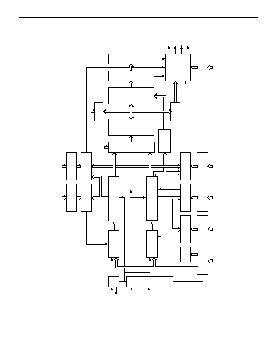
number of user selectable modes (Figure 1).
Notes:
All signals with a preceding front slash, "/", are ac-
tive Low. For example, B//W (WORD is active Low); /B/W
(BYTE is active Low, only).
Power connections follow conventional descriptions be-
low:
Connection
Circuit
Device
Power
V
CC
V
DD
Ground
GND
V
SS
Z90102/90103/90104
Zilog
40-Pin Low-Cost Digital Television Controller
DS97TEL1902
3
1
Figure 1. Functional Block Diagram
Counter
Timer
Counter
Timer
4, 6 or 8 KB
Program ROM
RESET
Oscillator
WDT
Port 3/
Interrupt
Port 6
Z8 CPU
Core
Port 2
256 Byte
Register File
Port 1
A8-15
AD0-7
PWM 1
14 -bit
PWM 6
to
PWM 8
6-bit
On-Screen
Display
Port 0
120 Byte
Character RAM
3 Kbyte
Character ROM
P27
P26
P25
P24
P23
P22
P21
P20
PWM 6
PWM 7
PWM 8
OSCIN
OSCOUT
HSYNC
VSYNC
VRED
VGREEN
VBLUE
VBLANK
XTAL1
XTAL2
/RESET
P30
P31
P34
P35
P36
P60
P61
P62
P63
P64
P65
AFCIN
PWM 1
PWM 9
to
PWM 11
8-bit
PWM 9
PWM 10
PWM 11
Z90102/90103/90104
40-Pin Low-Cost Digital Television Controller
Zilog
4
DS97TEL1902
PIN DESCRIPTION
Figure 2. 40-Pin Mask-ROM Plastic DIP
PWM1
P35
P36
P34
P31
P30
XTAL1
XTAL2
/RESET
P60
GND
P61
P62
VCC
P63
P64
P65
AFCIN
OSCIN
OSCOUT
PWM6
PWM7
PWM8
PWM9
PWM10
PWM11
P27
P26
P25
P24
P23
P22
P21
P20
VBLANK
VBLUE
VGREEN
VRED
VSYNC
HSYNC
21
Z90102
Z90103
Z90104
40-Pin DIP
1
20
40
Table 1. 40-Pin Mask-ROM Plastic DIP
40-Pin
Name
Function
Direction
1
PWM1
Pulse Width Modulator 1
Output
2, 3
P35-36
Port 3, Pins 5, 6
Output
4
P34
Port 3, Pin 4
Output
5
P31
Port 3, Pin 1
Input
6
P30
Port 3, Pin 0
Input
7
XTAL1
Crystal Oscillator
Input
8
XTAL2
Crystal Oscillator
Output
9
/RESET System
Reset
Input
10
P60
Port 6, Pin 0
Input
11
GND
Ground
Input
12
P61
Port 6, Pin 1
Input
13
P62
Port 6, Pin 2
Input
14
V
CC
Power Supply
Input
15, 16, 17
P63-65
Port 6, Pins 3, 4, 5
Input
18
AFC
IN
AFC Voltage Level
Input
19
OSC
IN
Video Dot Clock Osc
Input
20
OSC
OUT
Video Dot Clock Osc
Output
21
HSYNC
Horizontal Sync
Input
22
VSYNC
Vertical Sync
Input
23
Vred
Video Red
Output
Z90102/90103/90104
Zilog
40-Pin Low-Cost Digital Television Controller
DS97TEL1902
5
1
24
Vgreen
Video Green
Output
25
Vblue
Video Blue
Output
26
Vblank
Video Blank
Output
27-34
P20-27
Port 2, Pins 0,1,2,3,4,5,6,7
In/Output
35
PWM11
Pulse Width Modulator 11
Output
36
PWM10
Pulse Width Modulator 10
Output
37
PWM9
Pulse Width Modulator 9
Output
38
PWM8
Pulse Width Modulator 8
Output
39
PWM7
Pulse Width Modulator 7
Output
40
PWM6
Pulse Width Modulator 6
Output
Table 1. 40-Pin Mask-ROM Plastic DIP
40-Pin
Name
Function
Direction

Z90102/90103/90104
40-Pin Low-Cost Digital Television Controller
Zilog
6
DS97TEL1902
PIN DESCRIPTION
XTAL1, XTAL2.
(time-based input, output, respectively).
These pins connect to the internal parallel-resonant clock
crystal (4 MHz max) oscillator circuit with two capacitors
to GND. XTAL1 is also used as an external clock input.
SCLK System Clock.
SCLK is the internal system clock.
It can be used to clock external glue logic.
HSYNC
(input, Schmitt triggered, CMOS level). Horizontal
Sync is an input pin that accepts an externally generated
Horizontal Sync signal of either negative or positive polar-
ity.
VSYNC
(input,Schmitt-triggered, CMOS level). Vertical
Sync is an input pin that accepts an externally generated
Vertical Sync signal of either negative or positive polarity.
OSCIN, OSCOUT
(Video Oscillator input, output, respec-
tively). Oscillator input and output pins for on-screen dis-
play circuits. These pins connect to an inductor and two
capacitors to generate the character dot clock (typically
around 6 MHz). The dot clock frequency determines the
character pixel width and phase synchronized to HSYNC.
Vblank Video Blank
(output). CMOS output, programma-
ble polarity. Used as a superimpose control port to display
characters from video RAM. The signal controls Y signal
output of the CRT and turns off the incoming video display
while the characters in video RAM are superimposed on
the screen. The red, green, and blue outputs drive the
three electron guns on the CRT directly, while the blank
output turns off the Y signal.
Vblue Video Blue
(output). CMOS Output of the Blue vid-
eo signal (B-Y) and is programmable for either polarity.
Vgreen Video Green
(output). CMOS Output of the Green
video signal (G-Y) and is programmable for either polarity.
Vred Video Red
(output). CMOS Output of the Red video
signal (R-Y) and is programmable for either polarity.
Port 2
(P27-P20). Port 2 is an 8-bit port, CMOS-compati-
ble, bit programmable for either input or output. Input buff-
ers are Schmitt triggered. Bits programmed as outputs
may be globally programmed as either push pull or open-
drain (Figure 9).
Port 3
(P30, P31, P34-P36). Port 3, P30 input, is read di-
rectly. If appropriately enabled, a negative edge event is
latched in IRQ3 to initiate an IRQ3 vectored interrupt. An
application could place the device in STOP Mode when
P30 goes Low (in the IRQ3 interrupt routine). P30 initiates
a STOP Mode recovery when it subsequently goes to a
High. Port 3, P31 are read directly. If appropriately en-
abled, a negative edge event is latched in IRQ2 to initiate
an IRQ2 vectored interrupt. P31 High is signified as the
TIN signal to Timer1. Port 3, P34 and P35 are general-pur-
pose output lines. Port 3, P36 can be used as a general-
purpose output or as an output for TOUT (from Timer1 or
Timer2) or SCLK (Figure 10).
Port 6
(P65-P60). Port 6 is a 6-bit, Schmitt triggered
CMOS compatible, input port. The outputs of the AFC
comparators internally feed into the Port 6, bit 6 and bit 7
inputs (Figure 11).
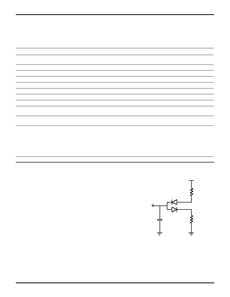
AFCIN
(Comparator input port, memory mapped). The in-
put signal is supplied to two comparators with VTH1=2/5
V
CC
and VTH2=3/5 V
CC
typical threshold voltage. The
comparator outputs are internally connected to Port 6, bit
6 and bit 7. AFCIN is typically used to detect AFC voltage
level to accommodate digital automatic fine tuning func-
tions (Figure 12).
Pulse Width Modulator 1
(PWM). PWM1 is typically used
as the D/A converter for Voltage Synthesis Tuning sys-
tems. It is a push-pull output with 14-bit resolution.
Pulse Width Modulator 6-8
(PWM). PWM8-PWM6 are
Pulse Width Modulators with 6-bit resolution.
Pulse Width Modulator 9, 10, 11
(PWM). Pulse Width
Modulator circuits with 8-bit resolution. These PWMs are
12 volt, open-drain outputs.
Pulse Width Modulator 1, 6, 7, 8
(PWM). Can be pro-
grammed as general-purpose outputs. PWM 1 is 5 V
OH
push-pull, and PWMs 6, 7, 8 are 12 volt open-drain out-
puts.
/RESET
System Reset. Code is executed from memory
address 000CH after the /RESET pin is set to a high level.
The reset function is also carried out by detecting a V
CC
transition state (automatic Power-On Reset) so that the
external reset pin can be permanently tied to V
CC
. A low
level on /RESET forces a restart of the device.
Z90102/90103/90104
Zilog
40-Pin Low-Cost Digital Television Controller
DS97TEL1902
7
1
ABSOLUTE MAXIMUM RATINGS
Stresses greater than those listed under Absolute Maxi-
mum Ratings may cause permanent damage to the de-
vice. This is a stress rating only; operation of the device at
any condition above those indicated in the operational sec-
tions of this specification is not implied. Exposure to abso-
lute maximum rating conditions for extended periods may
affect device reliability.
STANDARD TEST CONDITIONS
The characteristics listed below apply for standard test
conditions as noted. All voltages are referenced to GND.
Positive current flows into the referenced pin (Figure 3).
Symbol
Parameters Min
Max
Units
Notes
V
CC
Power Supply
Voltage*
≠0.3
+7
V
V
I
Input Voltage
≠0.3
V
CC
+0.3
V
V
I
Input Voltage
≠0.3
V
CC
+0.3
V
1
V
O
Output Voltage
≠0.3
13.2
V
2, 3
I
OH
Output Current High
≠10
mA
1 pin
I
OH
Output Current High
≠100
mA
All total
I
OL
Output Current Low
20
mA
1 pin
I
OL
Output Current Low
200
mA
All total
T
A
Operating
Temperature
T
STG
Storage
Temperature
≠65
+150
C
Notes:
1. Port 2 open-drain
2. PWM open-drain outputs
3. Absolute maximum operating voltage 13.2V.
Absolute maximum momentary (non-operating) voltage is 16.0V.
* Voltage on all pins with respect to GND.
See Ordering Information
Figure 3. Test Load Diagram
From Output
Under Test
RLL
VDD
RLH
150 pF

Z90102/90103/90104
40-Pin Low-Cost Digital Television Controller
Zilog
8
DS97TEL1902
CAPACITANCE
T
A
= 25
∞
C; V
CC
= GND = 0V; Freq =1.0 MHz; unmeasured pins to GND.
DC CHARACTERISTICS
T
A
= 0
∞
C to +70
∞
C; V
CC
= +4.5V to +5.5V; FOSC = 4 MHz
Parameter
Max
Units
Input capacitance
10
pF
Output
capacitance
20
pF
I/O capacitance
25
pF
AFCIN input
capacitance
10
pF
T
A
= 0
∞
C to +70
∞
C
Typical
Sym
Parameter
Min
Max
@ 25
∞
C
Units
Conditions
V
IL
Input Voltage Low
0
0.2 V
CC
1.48
V
V
ILC
Input XTAL/Osc In Low
0.07 V
CC
0.98
V
External Clock
Generator Driven
V
IH
Input Voltage High
0.7 V
CC
V
CC
3.0
V
V
IHC
Input XTAL/Osc In High
0.8 V
CC
V
CC
3.2
V
External Clock
Generator Driven
V
HY
Schmitt Hysteresis
0.1 V
CC
0.8
V
V
PU
Maximum Pull-Up
Voltage
13.2
V
1, 2
V
OL
Output Voltage Low
0.4
0.4
0.16
0.19
V
V
I
OL
=1.00 mA
I
OL
=0.75 mA 1
V
00-01
AFC Level 01 In
0.45 V
CC
1.9
V
V
01-11
AFC Level 11 In
0.5 V
CC
0.75 V
CC
3.12
V
V
OH
Output Voltage High
V
CC
≠0.4
4.75
V
I
OH
=≠0.75 mA
I
IR
Reset Input Current
≠80
≠46
m
A
V
RL
=0
V
II
L
Input Leakage
≠3.0
3.0
0.01
m
A
0V, V
CC
I
OL
Tristate Leakage
≠3.0
3.0
0.02
m
A
0V, V
CC
I
CC
I
CC1
I
CC2
Supply Current
20
6
10
13.2
3.2
2.0
mA
mA
m
A
All inputs at rail &
outputs floating
Notes:
1. PWM open-drain
2. Recommended operating voltage 12V with maximum positive
tolerance 10%, i.e., 13.2V.

Z90102/90103/90104
Zilog
40-Pin Low-Cost Digital Television Controller
DS97TEL1902
9
1
AC CHARACTERISTICS
Timing Diagrams
Figure 4. External Clock
XTAL1
2
2
1
3
3
Figure 5. Counter Timer
TIN
7
5
4
6
Figure 6. Interrupt Request
IRQN
8
9

Z90102/90103/90104
40-Pin Low-Cost Digital Television Controller
Zilog
10
DS97TEL1902
Figure 7. Power-On Reset
External /RESET
10
11
12
Internal /RESET
VCC
Figure 8. On-Screen Display
HSYNC
14
13
OSC2
Z90102/90103/90104
Zilog
40-Pin Low-Cost Digital Television Controller
DS97TEL1902
11
1
AC CHARACTERISTICS
T
A
= 0
∞
C to +70
∞
C; V
CC
= +4.5V to +5.5V; F
OSC
= 4 MHz
No
Symbol
Parameter
Min
Max
Unit
1
TpC
Input Clock Period
250
1000
ns
2
TrC,TfC
Clock Input Rise and Fall
15
ns
3
TwC
Input Clock Width
125
ns
4
TwTinL
Timer Input Low Width
70
ns
5
TwTinH
Timer Input High Width
3TpC
6
TpTin
Timer Input Period
8TpC
7
TrTin,TfTin
Timer Input Rise and Fall
100
ns
8a
TwIL
Int Req Input Low
70
ns
8b
TwIL
3TpC
9
TwIH
Int Request Input High
3TpC
10
TdPOR
Power On Reset Delay
25
100
ms
11
TdLVIRES
Low Voltage Detect to
200
ns
Internal RESET
Condition
12
TwRES
Reset Minimum Width
5TpC
13
TdHsOI
HSYNC Start to VOSC
Stop
2TpV
3TpV
14
TdHsOh
HSYNC End to VOSC
Start
1TpV
15
TdWDT
WDT Refresh Time
12
ms
Notes:
Refer to DC Characteristics for details on switching levels.

Z90102/90103/90104
40-Pin Low-Cost Digital Television Controller
Zilog
12
DS97TEL1902
FUNCTIONAL DESCRIPTION
The Z8 DTCincorporates special functions to enhance the
Z8's versatility in consumer, industrial and television con-
trol applications.
Pulse Width Modulator (PWM). The has seven PWM
channels (Figure 9). There are three types of PWM cir-
cuits: PWM1 (one channel of 14-bit resolution) typically
used for Voltage Synthesis Tuning, PWM8-PWM6 (three
channels of 6-bit resolution) typically used for audio level
control, and PWM9, 10, 11 (three channels of 8-bit resolu-
tion) typically used for picture level control. The PWM con-
trol registers are mapped into external memory and are ac-
cessed through LDE and LDEI instructions.
PWM1. It is a push-pull output.
PWMs 6 through 11. They have their maximum values
(on times) when all 1s are loaded in their PWM Value reg-
isters (and minimum value for all 0s). PWM1 has a maxi-
mum value for all 0s and minimum value for all 1s.
On-Screen Display (OSD). The OSD has a capability of
displaying 6 rows x 20 columns of 96 kinds of characters
for high resolution (11 x 15 dots) patterns (Figures 10 and
11).
Figure 9. Pulse Width Modulator Block Diagram
FC1Dh
FC1Ch
AD7-0
AD7-0
PWM Output
Port Reg
FC10h
FC11h
PWM Mod Reg
7-0
7-0
0
PWM1 push-pull
output
PWM6 (open-drain)
PWM7 (open-drain)
PWM8 (open-drain)
PWM9 (open-drain)
RSFF
MPX
RS & DFF
7-Bit
Comparator
Pulse
Distributor
14-Bit Binary
Down Counter
14-Bit
PWM1
Reg
FC12-3h
Upper 7-Bit
8-Bit
Comparator
8-Bit
PWM9
Reg
6-Bit
PWM6
Reg
FC18h
FC19h
FC1Ah
FC1Bh
6-0
13-7
13-7
6-0
13-0
Lower 7-Bit
5-0
5-0
7-0
7-0
7-0
AD7-0
AD7-0
AD7-0
XTAL
/RESET
5-0
RSFF
6-Bit
Comparator
RSFF
RSFF
RSFF
RSFF
PWM10 (open-drain)
PWM11 (open-drain)
Z90102/90103/90104
Zilog
40-Pin Low-Cost Digital Television Controller
DS97TEL1902
13
1
Figure 10. On-Screen Display Block Diagram
5-0
Horizontal Position
Register
FC02H
AD7-0
AD7-0
Bar Line Control
Register
FC06-7H
6-Bit
AD7-0
AD7-0
Comparator
Comparator
ADDR
BUS
MPX
Video
RAM
(20 x 6 x 7)
Character
Generator
ROM
(96 x 32 x 6)
Main
DOT
Shift
Reg
Sub
DOT
Shift
Reg
Data Bus
MPX
Row ATTR
Reg
Character DOT
& Smoothing
& Fringe
Generator
Address
INC/DEC/PASS
Control
Display Attribute
Register
FC03H
AD7-0
AD7-0
AD7-0
AD7-0
AD7-0
3-0
4-0
5-0
2-0
4-5
6
Column Address Counter
Reset
5-Bit
7-Bit
3-Bit
4-Bit
1/4
1/4
Horizontal Size
Counter
OSC
Reset
Polarity
Control
Vertical Size
Counter
Row Address Counter
Reset
Retrace
Timer
Comparator
Comparator
Comparator
OSD Control
Register
Vertical Position
Register
Row Space Control
Register
Fade Position
Register
FC00H
FC01H
FC04H
FC05H
OSCIN
OSCOUT
HSYNC
VSYNC
VBLANK
RED
GREEN
BLUE
HS
VS
VSYNC
IRQ
Enable
8-Bit
6-Bit

Z90102/90103/90104
40-Pin Low-Cost Digital Television Controller
Zilog
14
DS97TEL1902
FUNCTIONAL DESCRIPTION (Continued)
The OSD features are as follows:
s
Character Color: Seven kinds of color are specified on
a row basis.
s
Character Pixel Size: Four character pixel sizes are
selected for a high resolution (1HL, 2HL, 3HL, and 4HL)
Horizontal Line (HL).
s
Polarity Selections: Can select active low or high for
horizontal/vertical sync input and RGB outputs.
s
Display Position: Can display 64 vertical positions by
4HL units and 64 horizontal positions by a 4-dot clock.
s
Inter Row Spacing: Inter row vertical line spacing is set
from 2HL to 17HL.
s
Fade In/Out Control: Fade position can be determined
in vertical direction.
s
Bar Line Type Display: One of the rows is selected to
display an analog bar line every half column by setting
second color with proper character set.
s
Fringe Function: Fringe off/on and the color selected.
s
Background Color: Eight kinds of color including black
background color.
s
ON/OFF Control: Character display, backgrounds are
turned on and off.
s
Number of Display Characters: 6 rows x 20 columns.
s
Character Set: 96 (11 x 15 dots).
Character Generator ROM. The character generator
ROM is organized as 3 KB of six bits. The ROM defines ei-
ther 11 x 15 dot (high resolution)
Video RAM. The Video RAM is organized as 8-row arrays
(21 x 7 bits each, Figure 11). The first location of each row
array contains the attribute for that row. Row attributes in-
clude programmable character color, row background col-
or and control for background off/on. The next 20 bytes
contain row character data. Each character byte contains
the ASCII code in order to select one of the 96 displayable
characters. LDE or LDEI instructions are required to ac-
cess the Video RAM (Figure 11).
Figure 11. Video RAM Configuration
Hex
Address
FD00
FD01
FD02
FD13
FD14
Row 1 Attribute (ROW1_ATTR)
Row 1 Column 1 Character Data
Row 1 Column 2 Through
Column 19 Character Data
Row 1 Column 20 Character Data
Row 2 Attribute (ROW2_ATTR)
Row 2 Column 1 Character Data
Row 2 Column 2 Through
Column 19 Character Data
Row 2 Column 20 Character Data
FD20
FD21
FD22
FD33
FD34
Row 3 Video RAM Buffer
Row 4 Video RAM Buffer
Row 5 Video RAM Buffer
Row 6 Video RAM Buffer
FD40
FD54
FD60
FD74
FD80
FD94
FDA0
FDB4
MSB
(7 Bits Wide)
LSB
Z90102/90103/90104
Zilog
40-Pin Low-Cost Digital Television Controller
DS97TEL1902
15
1
Figure 12. Video RAM Map
(Write/Read Registers)
Row 1 Column 1 Character FD01H
Row 1 Column 2 Character FD02H
Row 1 Column 3 Character FD03H
Row 1 Column 4 Character FD04H
Row 1 Column 5 Character FD05H
Row 1 Column 6 Character FD06H
Row 1 Column 7 Character FD07H
Row 1 Column 8 Character FD08H
Row 1 Column 9 Character FD09H
Row 1 Column 10 Character FD0AH
Row 1 Column 11 Character FD0BH
Row 1 Column 12 Character FD0CH
Row 1 Column 13 Character FD0DH
Row 1 Column 14 Character FD0EH
Row 1 Column 15 Character FD0FH
Row 1 Column 16 Character FD10H
Row 1 Column 17 Character FD11H
Row 1 Column 18 Character FD12H
Row 1 Column 19 Character FD13H
Row 1 Column 20 Character FD14H
FD21H
FD22H
FD23H
FD24H
FD25H
FD26H
FD27H
FD28H
FD29H
FD2AH
FD2BH
FD2CH
FD2DH
FD2EH
FD2FH
FD30H
FD31H
FD32H
FD33H
FD34H
FD41H
FD42H
FD43H
FD44H
FD45H
FD46H
FD47H
FD48H
FD49H
FD4AH
FD4BH
FD4CH
FD4DH
FD4EH
FD4FH
FD50H
FD51H
FD52H
FD53H
FD54H
FD61H
FD62H
FD63H
FD64H
FD65H
FD66H
FD67H
FD68H
FD69H
FD6AH
FD6BH
FD6CH
FD6DH
FD6EH
FD6FH
FD70H
FD71H
FD72H
FD73H
FD74H
FD81H
FD82H
FD83H
FD84H
FD85H
FD86H
FD87H
FD88H
FD89H
FD8AH
FD8BH
FD8CH
FD8DH
FD8EH
FD8FH
FD90H
FD91H
FD92H
FD93H
FD94H
FDA1H
FDA2H
FDA3H
FDA4H
FDA5H
FDA6H
FDA7H
FDA8H
FDA9H
FDAAH
FDABH
FDACH
FDADH
FDAEH
FDAFH
FDB0H
FDB1H
FDB2H
FDB3H
FDB4H
Row 1 Attribute FD00H FD20H
FD40H
FD60H
FD80H
FDA0H
ROW1
ROW2
ROW3
ROW4
ROW5
ROW6
( 7 Bits Wide)
LSB
MSB

Z90102/90103/90104
40-Pin Low-Cost Digital Television Controller
Zilog
16
DS97TEL1902
FUNCTIONAL DESCRIPTION (Continued)
Figure 13. High Resolution Character ROM Configuration
0 1 1 0 0 0
1 1 1 0 0 0
0 0 1 0 0 0
0 0 1 0 0 0
0 1 0 1 0 0
0 0 1 0 0 0
1 0 0 0 1 0
0 1 1 0 0 0
1 0 0 0 1 0
0 0 1 0 0 0
0 0 0 0 0 0
0 0 1 0 0 0
1 1 1 1 1 0
1 1 1 1 1 0
0 0 1 0 0 0
0 0 1 0 0 0
0 0 1 0 0 0
1 0 1 0 1 0
1 1 1 1 1 0
1 0 1 0 1 0
0 0 1 0 0 0
1 0 1 0 1 0
1 0 1 0 1 0
0 1 1 1 0 0
0 1 1 1 0 0
1 0 1 0 1 0
00
01
02
03
04
05
06
07
08
09
0A
0B
0C
0D
0E
0F
10
11
12
13
14
15
16
17
18
19
1A
1B
1C
1D
1E
1F
Hex
Address
0 0 0 0 0 0
0 0 0 0 0 0
20
3F
0 0 1 0 0 0
1 0 1 0 1 0
1 1 1 1 1 0
1 0 1 0 1 0
Ø
High Resolution
Character Pattern
High Resolution
Character Pattern
High Resolution
Character Pattern
FC0
FDF
Ø
FE0
FFF
Ø
MSB
LSB
(6 Bits Wide)
Must be 00H
at each pattern
Left Half
Right Half

Z90102/90103/90104
Zilog
40-Pin Low-Cost Digital Television Controller
DS97TEL1902
17
1
Program Memory. The program ROM size is 6 KB (Figure
14). The IRQ vector table is located in the lower address
space. The vector address is fetched after the correspond-
ing interrupt and program control is passed to the specified
vector address. IRQ1 vector is fixed to VSYNC interrupt re-
quest and occurs at the leading edge of the filtered VSYNC
input. Program memory start at address 000CH after re-
set.
Figure 14. Program Memory
IRQ0 (High Byte)
IRQ0 (Low Byte)
VSYNC IRQ1 (High Byte)
VSYNC IRQ1 (Low Byte)
P31 IRQ2 (High Byte)
P31 IRQ2 (Low Byte)
P30 IRQ3 (High Byte)
P30 IRQ3 (Low Byte)
T0 IRQ4 (High Byte)
T0 IRQ4 (Low Byte)
T1 IRQ5 (High Byte)
T1 IRQ5 (Low Byte)
Reset Start Address
On-Chip Program ROM
(6 KByte)
Reserved
Memory Mapped I/O
Reserved
Video Refresh RAM
Reserved
0000
0001
0002
0003
0004
0005
0006
0007
0008
0009
000A
000B
000C
Ø
17FF
1800
Hex
Address
Ø
FBFF
FC00
Ø
FC32
FC33
Ø
FCFF
FD00
Ø
FDB4
FDB5
Ø
FFFF
OSD Control (OSD_CNTRL)
Vertical Position (VERT_POS)
Horizontal Position (HOR_POS)
Display Attribute (DISP_ATTR)
Row Space (ROW_SPACE)
Fade Position (FADE_POS)
Bar Line Control (BAR_CNTRL)
Bar Position (BAR_POS)
PWM Mode (PWM_MODE)
PWM Output Port (PWM_OUT)
PWM1 High 6-Bit (PWM1_HI)
PWM1 Low 8-Bit (PWM_LO)
PWM6 6-Bit Register (PWM6)
PWM7 6-Bit Register (PWM7)
PWM8 6-Bit Register (PWM8)
PWM9 8-Bit Register (PWM9)
FC01
Hex
Address
FC02
FC03
FC04
FC05
FC06
FC07
FC00
FC10
FC11
FC12
FC13
FC14
FC15
FC16
FC17
FC18
FC19
FC1A
FC1B
FC1C
FC1D
FC1E
FC1F
FC30
FC31
FC32
Port 6 Input Port (PORT6)
PWM10 8-Bit Register (PWM10)
PWM11 8-Bit Register (PWM11)
Reserved
Reserved
Reserved
Write
Only
Reserved
Z90102/90103/90104
40-Pin Low-Cost Digital Television Controller
Zilog
18
DS97TEL1902
FUNCTIONAL DESCRIPTION (Continued)
Memory Mapped Register. All control registers and I/O
ports (except Port 2 and Port 3) are assigned to program
memory space. Address space FC00H contains OSD con-
trol registers, PWM output registers and Port 6 I/O regis-
ters. Two bits of the decoded AFCIN port are assigned to
Port 6 input port. LDE and LDEI instructions are required
to transfer data between the Register File and the Memory
Mapped Registers.
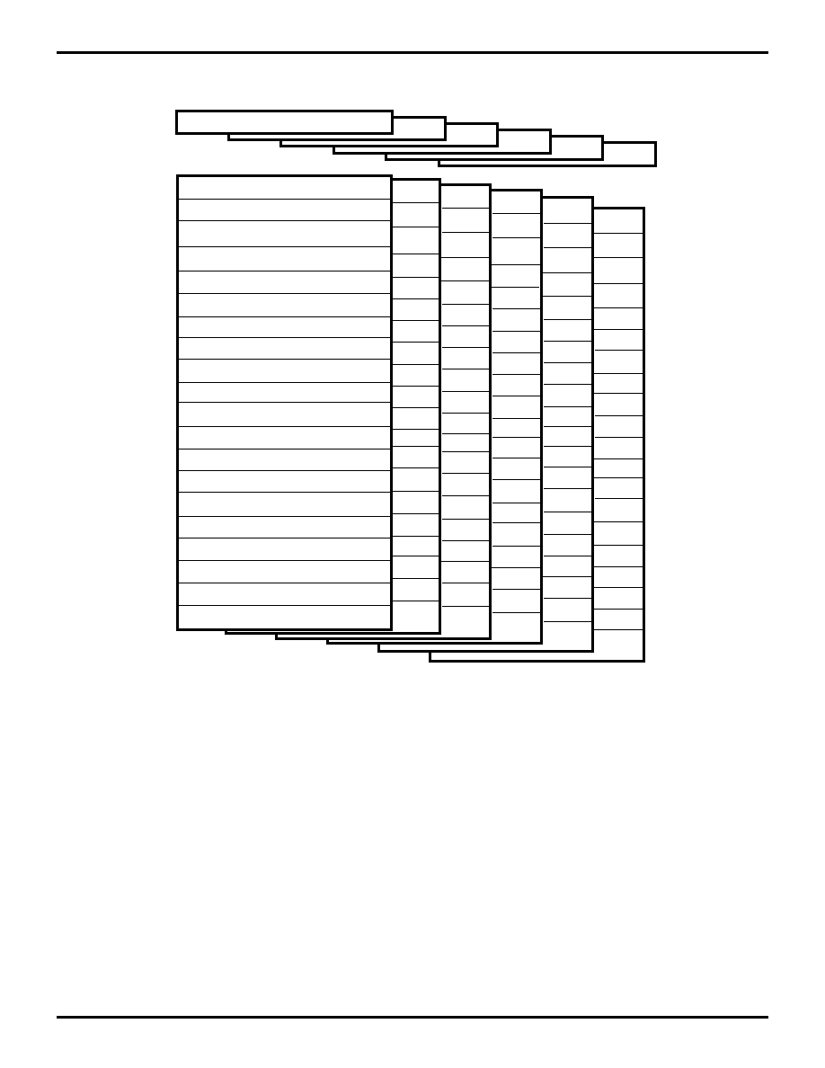
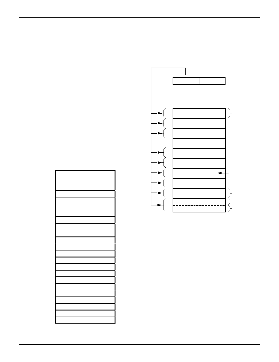
Register File. A total of 253 byte registers are implement-
ed in the Z8 core. Address 00H, 01H and FOH are re-
served. The register file consists of two I/O Port registers,
236 general-purpose registers and 15 control and status
registers (Figure 19). The instructions can access regis-
ters directly or indirectly with an 8-bit address field. This
also allows short 4-bit register addressing using the Reg-
ister Pointer. In the 4-bit mode, the register file is divided
into sixteen working-register groups, each occupying 16
continuous locations. The Register Pointer addresses the
starting location of the active working-register group (Fig-
ure 15).
Note: Register Bank E0-EF is only accessed through a
working register and indirect addressing modes.
Figure 15. Register File Configuration
Hex
Address
Port 2 (P2)
Port 3 (P3)
General-Purpose
Registers
Reserved
Timer Mode (TMR)
Timer/Counter1(T1)
T1 Prescaler (PRE1)
Timer/Counter0 (T0)
T0 Prescaler (PRE0)
Port 2 Mode (P2M)
Port 3 Mode (P3M)
Port 0-1 Mode (P01M)
Interrupt Priority Reg (IPR)
Interrupt Request Reg (IRQ)
Interrupt Mask Reg (IMR)
Condition Flag (FLAGS)
Register Pointer (RP)
Stack Pointer High (SPH)
Stack Pointer Low (SPL)
02
03
04
EF
F0
F1
F2
F3
F4
F5
F6
F7
F8
F9
FA
FB
FC
FD
FE
FF
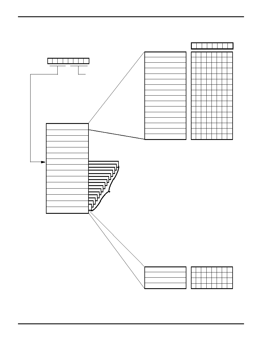
Figure 16. Register Pointer
The upper nibble of the register file address
provided by the register pointer specifies
the active working-register group.
r7 r6
r5 r4
R253
(Register Pointer)
I/O Ports
Specified Working
Register Group
The lower nibble
of the register
file address
provided by the
instruction points
to the specified
register.
r3 r2
r1 r0
Register Group 1
Register Group 0
R15 to R0
Register Group F
R15 to R4
R3 to R0
R15 to R0
∑
∑
∑
∑
∑
FF
F0
0F
00
1F
10
2F
20
∑
∑
∑
∑
∑
∑
∑
∑
∑
Z90102/90103/90104
Zilog
40-Pin Low-Cost Digital Television Controller
DS97TEL1902
19
1
Figure 17. Z90102/3/4 Register File Reset Condition
7
6
5
4
0
0
0
0
Working Register
Group Pointer
Must be "0"
%FF
%FO
%7F
%0F
%00
Z8 Reg. File
REGISTER POINTER
% FF
% FE
% FD
% FC
% FB
% FA
% F9
% F8
% F7
% F6
% F5
% F4
% F3
% F2
% F1
% F0
SPL
6P
RP
FLAGS
IMR
IRQ
IPR
Reserved
P3M
P2M
PRE0
T0
PRE1
T1
TMR
0
0
U
1
U
U
U
U
U
0
U
1
U
U
U
U
U
0
U
1
U
U
U
U
U
0
U
1
U
U
U
U
U
0
U
1
U
U
U
U
U
0
U
1
U
U
U
U
U
0
U
1
U
U
0
U
U
0
U
1
0
U
0
U
U
1
1
1
U
U
U
U
U
U
U
U
U
U
U
REGISTER
EXPANDED REG. GROUP (0)
RESET CONDITION
REGISTER
Z8 STANDARD CONTROL REGISTERS
RESET CONDITION
% (0) 03
P3
% (0) 02
P2
% (0) 01
Reserved
% (0) 00
Reserved
U = Unknown
D7
D6 D5 D4 D3 D2 D1 D0
Reserved
Reserved
Legend:
U
U
U
U
U
U
U
U
U
U
U
U
U
U
U
U
U
0
0
0
0
0
0
0
0
0
0
0
0
0
0
0
0
0
1
1
0
1
1
0
1
Note: All General-Purpose registers, PWM Registers,
and Video RAM registers, Port 4, 5, and 6
registers are undefined after reset.
U
U
U
U
U
U
U
U
U
U
U
U
U
U
U
U
Z90102/90103/90104
40-Pin Low-Cost Digital Television Controller
Zilog
20
DS97TEL1902
FUNCTIONAL DESCRIPTION (Continued)
Stack. Either the internal register file or the external data
memory is used for the stack. An 8-bit Stack Pointer is
used for the internal stack that resides within the 236 gen-
eral-purpose registers.
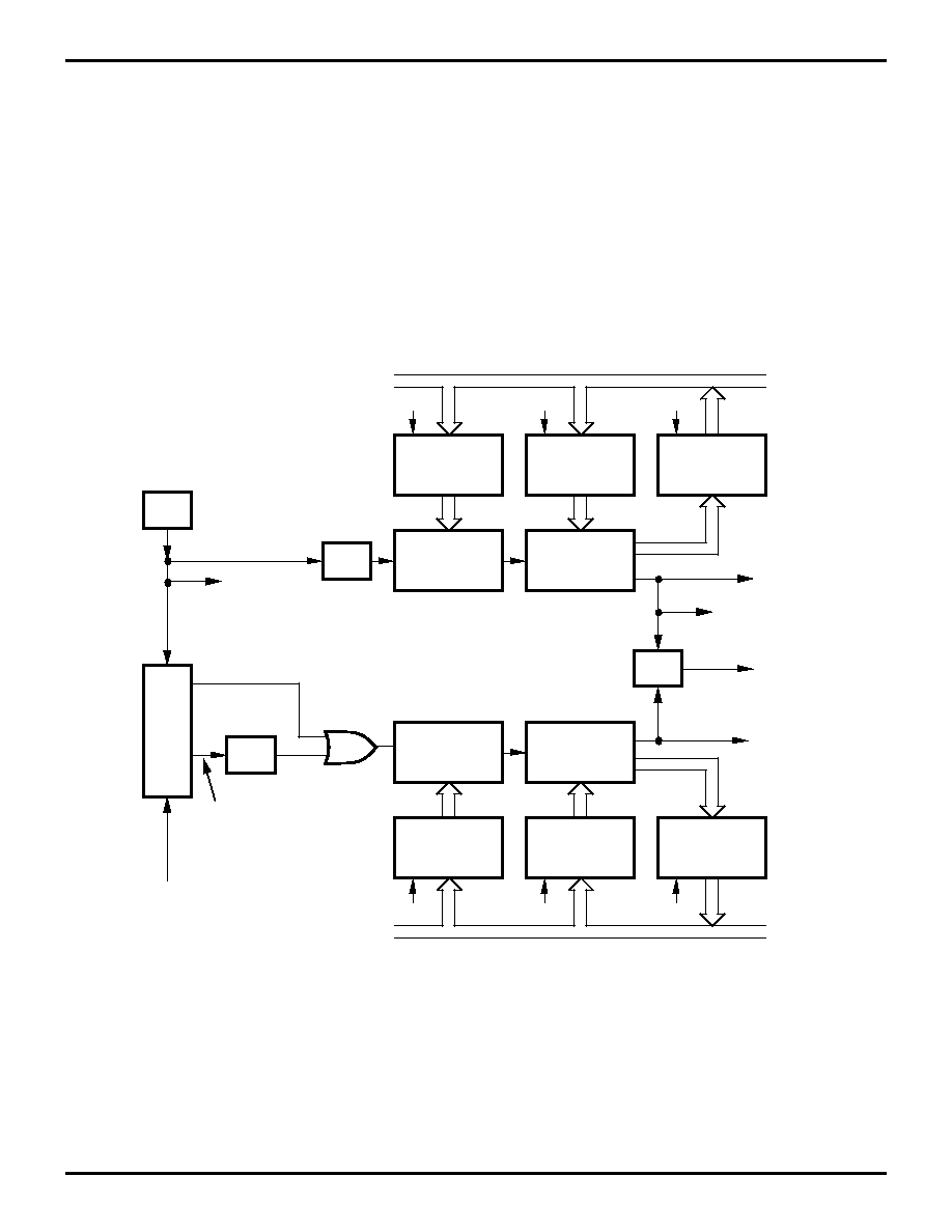
Counter/Timers. There are two 8-bit programmable
counter/timers (T0-T1), each driven by its own 6-bit pro-
grammable prescaler (PRE0 and PRE1). The T1 prescaler
can be driven by internal or external clock sources; howev-
er, the T0 prescaler is driven by the internal clock only (Fig-
ure 18).
The counter, but not the prescalers, are read at any time
without disturbing their value or count mode. The clock
source for T1 is user definable and is the internal micropro-
cessor clock (XTAL clock/4), or an external signal input
through Port 3, P31. The counter/timers are programmably
cascaded by connecting the T0 output to the input of T1.
Figure 18. Counter/Timer Block Diagram
OSC
PRE0
Initial Value
Register
T0
Initial Value
Register
T0
Current Value
Register
6-Bit
Down
Counter
8-Bit
Down
Counter
∏
4
6-Bit
Down
Counter
8-Bit
Down
Counter
PRE1
Initial Value
Register
T1
Initial Value
Register
T1
Current Value
Register
Clock
Logic
IRQ4
TOUT
P36
IRQ5
Internal Data Bus
Write
Write
Read
Internal Clock
Gated Clock
Triggered Clock
TIN P31
Write
Write
Read
Internal Data Bus
External Clock
Internal
Clock
∏
4
∏
2
Serial I/O
Clock
Z90102/90103/90104
Zilog
40-Pin Low-Cost Digital Television Controller
DS97TEL1902
21
1
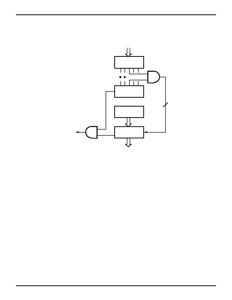
Interrupts. The DTC has six different interrupts from six
different sources. These interrupts are maskable and pri-
oritized (Figure 19). The six sources are divided as follows:
two sources are claimed by Port 3 (P30, P31), one by
VSYNC, two by the counter/timers, and one is software
triggered only.
Figure 19. Interrupt Block Diagram
IRQ
IMR
IPR
Priority
Logic
6
Global
Interrupt
Enable
Vector Select
Interrupt
Request
IRQ
Z90102/90103/90104
40-Pin Low-Cost Digital Television Controller
Zilog
22
DS97TEL1902
FUNCTIONAL DESCRIPTION (Continued)
HALT Mode. The Z90102/3/4 is driven by two internal
clocks, TCLK and SCLK. They both oscillate at the crystal
frequency. TCLK provides the clock signal for the counter-
timers and the interrupt block. SCLK provides the clock
signal for all other CPU blocks. HALT Mode turns off the
internal CPU clock (SCLK), but not the XTAL oscillation.
The counter/timers and external interrupts remain active.
The device may be recovered by interrupts, either exter-
nally or internally generated. An interrupt request may be
executed (enabled) to exit HALT Mode. After the interrupt
service routine, the program continues from the instruction
after the HALT.
STOP Mode. The STOP instruction stops crystal oscilla-
tion, thereby stopping both SCLK and TCLK. The device
ceases to operate. The STOP Mode can be released by
two methods. The first method is to reset the device. A
high input condition on Port 3 P30 is the second method.
After releasing the STOP Mode by using either one of the
two methods, program execution begins at location
000CH. To complete an instruction prior to entering the
standby modes, a NOP instruction has to be placed before
the HALT or STOP instructions. This is required because
of instruction pipelining, i.e.:
Notes: In STOP Mode, XTAL2 pin has an internal pull-up
on it and OSCOUT has an internal pull-down.
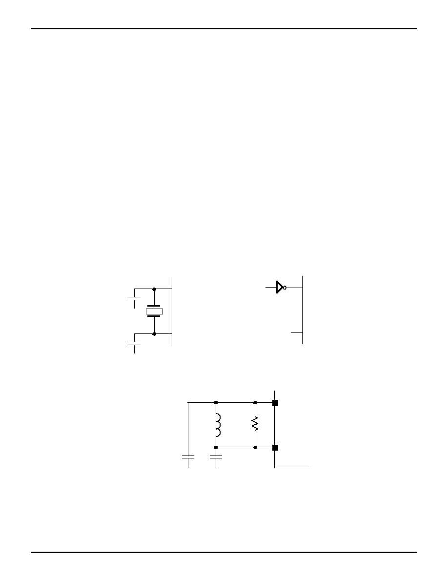
Clock. The Z90102/3/4 on-chip oscillator has a high-gain,
parallel-resonant amplifier for connection to a crystal, ce-
ramic resonator, or any suitable external clock source
(XTAL1 = Input, XTAL2 = Output). The crystal is an AT cut,
parallel resonant, 4 MHz max with a series resistance (RS)
less than or equal to 100 Ohms.
The crystal source is connected across XTAL1 and XTAL2
using the crystal manufacturer's recommended capacitors
(10 pF < CL < 300 pF, where C1=C2=CL) from each pin to
device ground (Figure 20).
FF NOP
; clear the pipeline
6F STOP
; enter STOP Mode
or
FF NOP
; clear the pipeline
7F HALT
; enter HALT Mode
Figure 20. Oscillator Configuration
XTAL1
XTAL2
C1
C2
33pF
33pF
XTAL1
XTAL2
XTAL1
XTAL2
Ceramic Resonator
or Crystal
External Clock
27
m
H
6.8k
W
MPU
LC Oscillator Circuits
* VSS
* VSS
* VSS
* VSS
* Must be connected to VSS pin and not
system ground.
Z90102/90103/90104
Zilog
40-Pin Low-Cost Digital Television Controller
DS97TEL1902
23
1
Watch-Dog Timer (WDT). The Z90102/3/4 is equipped
with a permanently enabled Watch-Dog Timer which must
be refreshed every 12 ms. Failure to refresh the timer re-
sults in a reset of the device. The WDT is permanently en-
abled and is initially reset upon POR. Every subsequent
WDT instruction resets the timer. The Watch-Dog Timer
may or may not be enabled during the STOP Mode. The
instruction WDT 4F (HEX) enables the timer during HALT.
If the WDH instruction is used, and if the HALT Mode is not
released and the Watch-Dog Timer is not retriggered (by
the WDT instruction) within 12 ms, a device reset occurs.
The WDT instruction affects the Z (Zero) S (Sign), and V
(Overflow) flags. WDT does not run during STOP Mode.
V
CC
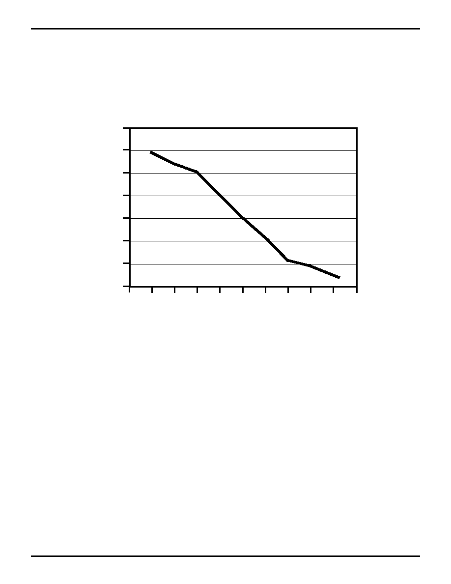
Voltage Sensitive Reset (VSR). Reset is globally
driven if V
CC
is below the specified voltage (Figure 21).
Figure 21. Voltage Sensitive Reset vs Temperature
-60
-40
-20
+0
20
40
60
80
100
120
140
VBO
3.60
3.40
3.20
3.00
2.80
2.60
2.40
Temperature
(
∞
C)
3.80
Z90102/90103/90104
40-Pin Low-Cost Digital Television Controller
Zilog
24
DS97TEL1902
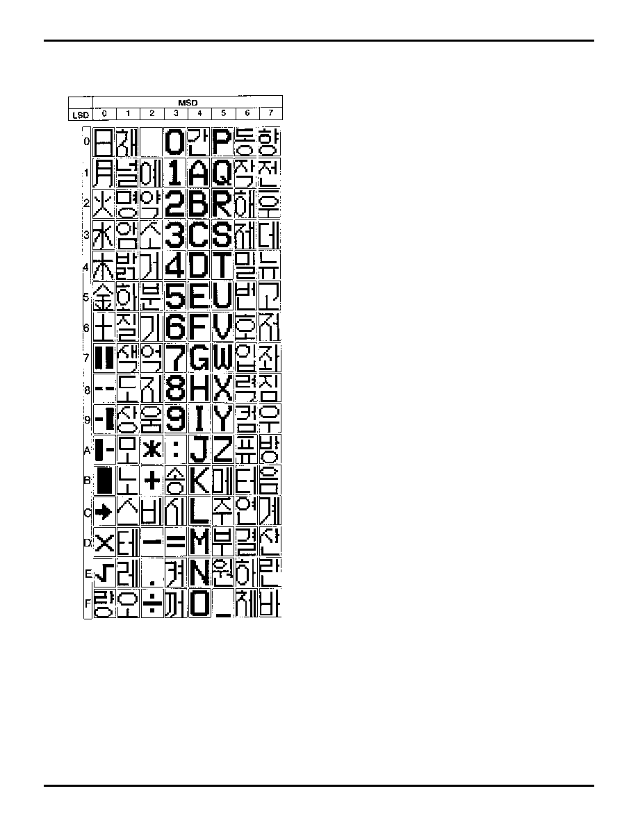
STANDARD CHARACTER SETS
Z90102/90103/90104
Zilog
40-Pin Low-Cost Digital Television Controller
DS97TEL1902
25
1
SUMMARY
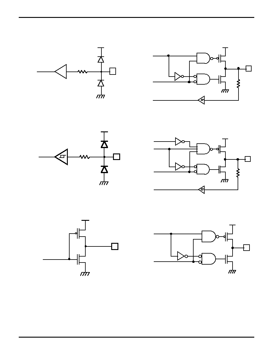
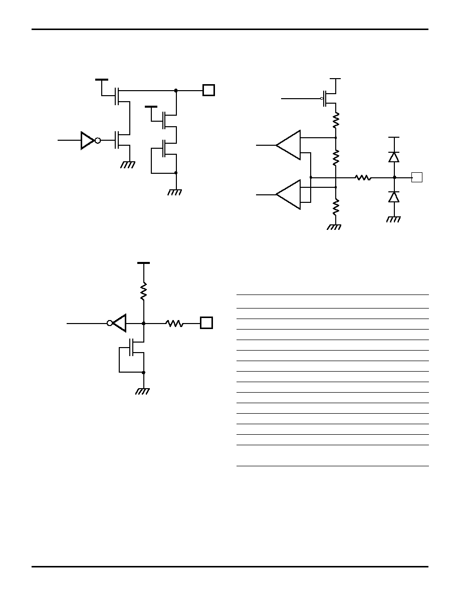
Input/Output Circuits
Figure 22. Input Only
(Pad Type 1)
Figure 23. Input Only, Schmitt-Triggered
(Pad Type 2)
Figure 24. Output Only
(Pad Type 3)
IN
20 Ohm
VCC
PAD
IN
20 Ohm
VCC
PAD
VCC
PAD
P
N
OUT
Figure 25. Input/Output Tristate
(Pad Type 4)
Figure 26. Input/Output, Tristate, Open-Drain
Figure 27. Output Only, Tristate
VCC
PAD
P
N
IN
OEN
OUT
20
Ohm
VCC
PAD
P
N
IN
OEN
OUT
20
Ohm
OD
VCC
PAD
P
N
OEN
OUT
Z90102/90103/90104
40-Pin Low-Cost Digital Television Controller
Zilog
26
DS97TEL1902
SUMMARY (Continued)
Figure 28. Output Only, 12-Volt Open-Drain
(Pad Type 7)
Figure 29. Reset Input Circuit
(Pad Type 8)
PAD
N
N
OUT
N
VCC
N
VCC
PAD
RESET
N
VCC
20 Ohm
RPU
Figure 30. AFC Input Circuit
(Pad Type 9)
Table 2. Mapping of Symbolic Pad Types to Pin
Functions
Pin Name
Pad Type
XTAL1, OSCIN
1
XTAL2, OSCOUT
*
/RESET
8
P20-P27
5
P30-P31
2
P34-P36
3
P60-P65
2
AFCIN
9
HSYNC, VSYNC
2
VRED, VBLUE, VGREEN,
3
VBLANK
3
PWM1
3
PWM [6 -11]
7
Note:
*High gain start, low gain run amplifier circuit.
VCC
P
20 Ohm
PAD
VCC
STOP
P67
P66
2R
1R
2R
-
+
-
+
Z90102/90103/90104
Zilog
40-Pin Low-Cost Digital Television Controller
DS97TEL1902
27
1
DTC CONTROL REGISTER DIAGRAMS
Port Registers
Figure 31. Port 2 Register
(Read/Write)
Figure 32. Port 2 Mode Register
(Write Only)
Input/Output Port
0 Logic Level 0
1 Logic Level 1
P2
02H
D7
D6
D5
D4
D3
D2
D1
D0
Input/Output Mode
0 Output Mode
1 Input Mode
P2M
F6H
D7 D6 D5 D4 D3 D2 D1 D0
Figure 33. Port 3 Register
(P30, P31 Read Only)
(P34, P35, P36 Write Only)
Figure 34. Port 6 Register
(Read Only)
P3
03H
D7
D6
D5
D4
D3
D2
D1
D0
P30 Input Port
Stop-Mode Recovery Input
P31 Input/T1 (input)
P34 Output Port
P35 Output Port
Reserved
P36 Output/T1, T0 (output)
P6
FC32H
D7 D6
D5
D4
D3
D2
D1
D0
Port 6 Input
0 Logic Level 0
1 Logic Level 1
Port 6 Comparator Input
00 GND thru V1
0 1 V1 thru V2
11 V2 thru VCC
Z90102/90103/90104
40-Pin Low-Cost Digital Television Controller
Zilog
28
DS97TEL1902
DTC CONTROL REGISTER DIAGRAMS
PWM Registers
Figure 35. PWM 1 High Value
(Write Only)
Figure 36. PWM 1 Low Value
(Write Only)
Figure 37. PWM 6 Value
(Write Only)
Figure 38. PWM 7 Value
(Write Only)
PWM1 UPPER
FC12H
D7
D6
D5
D4
D3
D2
D1
D0
PWM1 High Byte
Reserved (Must be 0)
PWM1 LOWER
FC13H
D7 D6
D5
D4
D3
D2
D1
D0
PWM1 Low Byte
PWM6 VAL
FC18H
D7 D6
D5
D4
D3
D2
D1
D0
PWM6 Value
Reserved (Must be 0)
PWM7 VAL
FC19H
D7 D6
D5
D4
D3
D2
D1
D0
PWM7 Value
Reserved (Must be 0)
Figure 39. PWM 8 Value
(Write Only)
Figure 40. PWM 9 Value
(Write Only)
Figure 41. PWM 10 Value
(Write Only)
Figure 42. PWM 11 Value
(Write Only)
PWM8 VAL
FC1AH
D7 D6
D5
D4
D3
D2
D1
D0
PWM8 Value
Reserved (Must be 0)
PWM9 VAL
FC1BH
D7 D6 D5 D4 D3 D2 D1 D0
PWM9 Value
PWM10 VAL
FC1CH
D7 D6
D5
D4
D3
D2
D1
D0
PWM10 Value
PWM11 VAL
FC1DH
D7 D6 D5 D4 D3 D2 D1 D0
PWM11 Value

Z90102/90103/90104
Zilog
40-Pin Low-Cost Digital Television Controller
DS97TEL1902
29
1
Figure 43. PWM Mode Register
(Write Only)
PWM MODE
FC10H
Reserved (Must be 0)
Mode Control
0 PWM
1 Output Port
D7 D6 D5 D4 D3 D2 D1 D0
Figure 44. PWM Port Output Register
(Write Only)
PWM OUT
FC11H
D7 D6
D5
D4
D3
D2
D1
D0
Reserved (Must be 0)
Output Control
0 = Logic Level 1
1 = Logic Level 0
Z90102/90103/90104
40-Pin Low-Cost Digital Television Controller
Zilog
30
DS97TEL1902
Z8 REGISTER DIAGRAMS
Figure 45. OSD Control Register
(Write Only)
Figure 46. OSD Vertical Position Register
(Write Only)
Figure 47. OSD Horizontal Position Register
(Write Only)
OSDC CNTRL
FC00H
D7 D6
D5
D4
D3
D2
D1
D0
Retrace Blanking
High Resolution
Must be 1
X4HL
Reserved (Must be 0)
Pixel Size
00 x 1
01 x 2
10 x 3
11 x 4
Sync Polarity
0 Positive
1 Negative
VERT POS
FC01H
D7 D6
D5
D4
D3
D2
D1
D0
Vertical Position Control
x 4 Horizontal Lines
Reserved (Must be 0)
HOR POS
FC02H
D7 D6
D5
D4
D3
D2
D1
D0
Horizontal Position Control
x 4 DOT Clocks
Reserved (Must be 0)
Figure 48. OSD Display Attribute Register
(Write Only)
Figure 49. OSD Row Space Register
(Write Only)
Figure 50. OSD Fade Position Register
(Write Only)
DISP ATTR
FC03H
D7 D6
D5
D4
D3
D2
D1
D0
RGB Polarity
0 - Positive
1 - Negative
Blue Background
Green Background
Red Background
Fringe On-Off
0 - Off
1 - On
Background On-Off
0 - Off
1 - On
Display On-Off
0 - Off
1 - On
Reserved (Must be 0)
ROW SPACE
FC04H
D7 D6
D5
D4
D3
D2
D1
D0
Inter Row Space
Fade On-Off
0 - Off
1 - On
Fade Direction
0 - Fade After
1 - Fade Before
Reserved (Must be 0)
FADE POS
FC05H
D7 D6
D5
D4
D3
D2
D1
D0
Vertical Index
Reserved (Must be 0)
Z90102/90103/90104
Zilog
40-Pin Low-Cost Digital Television Controller
DS97TEL1902
31
1
Figure 51. OSD Bar Control Register
(Write Only)
Figure 52. OSD Bar Position Register
(Write Only)
Figure 53. Timer Mode Register
(F1H: Read/Write)
Row Address
BAR CNTRL
FC06H
Red Bar Color
Green Bar Color
Blue Bar Color
Bar Color Enable
Reserved (Must be 0)
D7 D6
D5
D4
D3
D2
D1
D0
BAR POS
FC07H
D7 D6
D5
D4
D3
D2
D1
D0
Bar Column Position
Reserved (Must be 0)
R241 TMR
F1H
D7 D6
D5
D4
D3
D2
D1
D0
0 - No Function
1 - Load T0
0 -Disable T0 Count
1 -Enable T0 Count
0 - No Function
1 - Load T1
0 - Disable T1 Count
1 - Enable T1 Count
TIN Modes
00 External Clock Input
01 Gate Input
10 Trigger Input
(Non-retriggerable)
11 Trigger Input
(Retriggerable)
TOUT Modes
00 Not Used
01 T0 Out
10 T1 Out
11 Internal Clock Out
Figure 54. ROW_ATTR Register
(Write Only)
Figure 55. Counter Timer 1 Register
(F1H: Read/Write)
Figure 56. Prescaler 1 Register
(F3H: Write Only)
ROW_ ATTR
D7 D6
D5
D4
D3
D2
D1
D0
Row Background Color
Red
Green
Blue
Row Background On-Off
0 Off
1 On
Character Color
Red
Green
Blue
Reserved (Must be 0)
FD00H,FD20H,FD40H,
FD60H,FD80H,FDA0H
R242 T1
F2H
D7 D6
D5
D4
D3
D2
D1
D0
T1 Initial Value
(When Written)
(Range: 1-256 Decimal
01-00 Hex)
T1 Current Value
(When Read)
R243 PRE1
F3H
D7 D6
D5
D4
D3
D2
D1
D0
Count Mode
0 T1 Single Pass*
1 T1 Modulo N
Clock Source
1 T1 Internal
0 T1 External Timing Input*
(TIN) Mode
Prescaler Modulo
(Range: 1-64 Decimal
01-00 Hex)
* Default After Reset
Z90102/90103/90104
40-Pin Low-Cost Digital Television Controller
Zilog
32
DS97TEL1902
Z8 REGISTER DIAGRAMS (Continued)
Figure 57. Counter/Timer 0 Register
(F4H: Read/Write)
Figure 58. Prescaler 0 Register
(F5H: Write Only)
Figure 59. Port 2 Mode Register
(F6H: Write Only)
R244 T0
F4H
D7 D6
D5
D4
D3
D2
D1
D0
T0 Initial Value
(When Written)
(Range: 1-256 Decimal
01-00 Hex)
T0 Current Value
(When Read)
R245 PRE0
F5H
D7 D6
D5
D4
D3
D2
D1
D0
Count Mode
0 T0 Single Pass*
1 T0 Modulo-N
Reserved (Must be 0)
Prescaler Modulo
(Range: 1-64 Decimal
01-00 Hex)
* Default After Reset
R246 P2M
F6H
D7 D6
D5
D4
D3
D2
D1
D0
P27 - P20 I/O Definition
0 Defines Bit as Output
1 Defines Bit as Input
Figure 60. Port 3 Mode Register
(F6H; Write Only)
Figure 61. Interrupt Priority Register
(F9H: Write Only)
R247 P3M
F7H
D7 D6
D5
D4
D3
D2
D1
D0
0 - Port 2 Open-Drain
1 - Port 2 Push-Pull
Reserved (Must be 0)
0 P32 - Input P35 - Output
(Must be 0)
00 P33 - Input P34 - Output
(Must be 0)
11 Reserved
0 P31 - Input (TIN) P36 - Output (TOUT)
0 P30 - Input
Reserved (Must be 0)
R249 IPR
F9H
D7 D6
D5
D4
D3
D2
D1
D0
Interrupt Group Priority
000 Reserved
001 C > A > B
010 A > B > C
011 A > C > B
100 B > C > A
101 C > B > A
110 B > A > C
111 Reserved
IRQ1, IRQ4 Priority (Group C)
0 IRQ1 > IRQ4
1 IRQ4 > IRQ1
IRQ1, IRQ2 Priority (Group B)
0 IRQ2 > IRQ0
1 IRQ0 > IRQ2
IRQ3, IRQ5 Priority (Group A)
0 IRQ5 > IRQ3
1 IRQ3 > IRQ5
Reserved (Must be 0)

Z90102/90103/90104
Zilog
40-Pin Low-Cost Digital Television Controller
DS97TEL1902
33
1
Figure 62. Interrupt Request Register
(FAH: Read/Write)
Figure 63. Interrupt Mask Register
(FBH: Read/Write)
Figure 64. Flag Register
(FCH: Read/Write)
R250 IRQ
FAH
D7 D6
D5
D4
D3
D2
D1
D0
IRQ - Software only
IRQ1 - VSYNC
IRQ2 - P31 Input
IRQ3 - P30 Input
IRQ4 - T0
IRQ5 - T1
Reserved (Must be 0)
Reset Condition = 00H
R251 IMR
FBH
D7 D6
D5
D4
D3
D2
D1
D0
1 - Enables IRQ5 - IR0
(D0 - IRQ0)
Reserved (Must be 0)
1 - Enables Interrupts
0* Disable Interrupts
* Default after Reset
R252 FLAGS
FCH
D7 D6
D5
D4
D3
D2
D1
D0
User Flag F1
User Flag F2
Half Carry Flag
Decimal Adjust Flag
Overflow Flag
Sign Flag
Zero Flag
Carry Flag
Figure 65. Register Pointer
(FDH: Read/Write)
Figure 66. General-Purpose
(FEH: Read/Write)
Figure 67. Stack Pointer
(FFH: Read/Write)
R253 RP
FDH
D7 D6
D5
D4
D3
D2
D1
D0
Reserved (Must be 0)
Register Pointer
Reset Condition = 00H
R254 GP
FEH
D7 D6
D5
D4
D3
D2
D1
D0
0 = Level 0
1 = Level 1
Reset Condition = Undefined
R255 SPL
FFH
D7 D6
D5
D4
D3
D2
D1
D0
Stack Pointer Upper
Byte (SP7-SP0)
Z90102/90103/90104
40-Pin Low-Cost Digital Television Controller
Zilog
34
DS97TEL1902
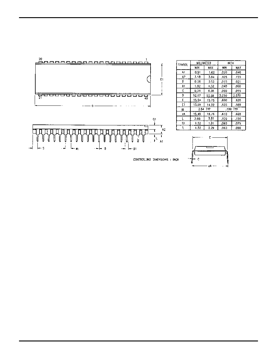
PACKAGE INFORMATION
Figure 68. 40-Pin DIP Package Diagram
Z90102/90103/90104
Zilog
40-Pin Low-Cost Digital Television Controller
DS97TEL1902
35
1
ORDERING INFORMATION
Z90102, Z90103, Z90104
4 MHz
40-pin DIP
Z90102/3/404PSC
For fast results, contact your local Zilog sales office for as-
sistance in ordering the part desired.
CODE
Package
P = Plastic DIP
Temperature
S = 0
∞
C to +70
∞
C
Speed
04 = 4 MHz
Environmental
C = Plastic Standard
Example:
Z 890103 04 P S C
is an 86227, 4 MHz, DIP, 0
∞C to +70∞C, Plastic Standard Flow
Environmental Flow
Temperature
Package
Speed
Product Number
Zilog Prefix

Z90102/90103/90104
40-Pin Low-Cost Digital Television Controller
Zilog
36
DS97TEL1902