 | –≠–ª–µ–∫—Ç—Ä–æ–Ω–Ω—ã–π –∫–æ–º–ø–æ–Ω–µ–Ω—Ç: ZMD31050 | –°–∫–∞—á–∞—Ç—å:  PDF PDF  ZIP ZIP |
Copyright © 2005, ZMD AG, Rev. 0.95, 2005-09-16
1/20
All rights reserved. The material contained herein may not be reproduced, adapted, merged, translated, stored, or used without the prior
written consent of the copyright owner. The Information furnished in this publication is preliminary and subject to changes without notice.
ZMD31050
Advanced Differential Sensor Signal Conditioner
Datasheet
PRELIMINARY
Features
∑
Digital compensation of sensor offset, sensitivity,
temperature drift and non-linearity
∑
Accommodates nearly all bridge sensor types
(signal spans from 1 up to 275mV/V processable)
∑
Digital one-shot calibration: quick and precise
∑
Selectable compensation temperature T1 source:
bridge, thermistor, internal diode or external diode
∑
Output options: voltage (0...5V), current
(4...20mA), PWM, I
2
C, SPI, ZACwire
TM
(one-wire-
interface), alarm
∑
Adjustable output resolution (up to 15 bits) versus
sampling rate (up to 3.9kHz)
∑
Selectable bridge excitation: ratiometric voltage,
constant voltage or constant current
∑
Input channel for separate temperature sensor
∑
Sensor connection and common mode check
(Sensor aging detection)
∑
operation temperature, depending on product
version, up to -40...+125∞C (-40...+150∞C derated)
∑
Supply voltage +2.7V...+5.5V
∑
Available in SSOP16 or as die
Benefits
∑
No external trimming components required
∑
PC-controlled configuration and calibration via
digital bus interface - simple, low cost
∑
High accuracy (±0.1% FSO @ -25...85∞C; ±0.25%
FSO @ -40...125∞C)
Brief Description
ZMD31050 is a CMOS integrated circuit for highly-
accurate amplification and sensor-specific correction
of bridge sensor signals. The device provides digital
compensation of sensor offset, sensitivity, temperature
drift and non-linearity by a 16-bit RISC micro controller
running
a
correction
algorithm
with correction
coefficients stored in non-volatile EEPROM.
The ZMD31050 accommodates virtually any bridge
sensor (e.g. piezo-resistive, ceramic-thickfilm or steel
membrane based). In addition, the IC can interface a
separate temperature sensor.
The
bi-directional
digital
interfaces
(I
2
C,
SPI,
ZACwire
TM
) can be used for a simple PC-controlled
one-shot calibration procedure, in order to program a
set of calibration coefficients into an on-chip
EEPROM. Thus a specific sensor and a ZMD31050
are mated digitally: fast, precise and without the cost
overhead
associated
with
laser
trimming,
or
mechanical potentiometer methods.
ß
Application kit available (SSOP16 samples,
calibration PCB, calibration software, technical
documentation)
ß
Support for industrial mass calibration
available
ß
Quick circuit customization possible for large
production volumes
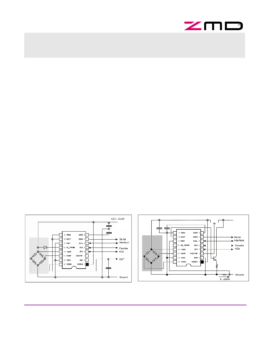
Application Circuit (Examples)
Fig.1: Ratiometric measurement with voltage output,
temperature compensation via external diode
R
e
R
sens
Refer also chapter 2 for additional application circuits and details
Fig.2: Two-wire-(4 to 20) mA configuration [(7 to 40) V],
temperature compensation via internal diode
V
SUPP
+7...+40 V
100
nF
100
nF
VDDA = 5 V
(50 )
(120 )
100 nF
100 nF
V
SUPP
15 nF

Copyright © 2005, ZMD AG, Rev. 0.95, 2005-09-16
2/20
All rights reserved. The material contained herein may not be reproduced, adapted, merged, translated, stored, or used without the prior
written consent of the copyright owner. The Information furnished in this publication is preliminary and subject to changes without notice.
ZMD31050
Advanced Differential Sensor Signal Conditioner
Datasheet
PRELIMINARY
Contents
1.
CIRCUIT DESCRIPTION ........................................................................................................... 3
1.1
S
IGNAL
F
LOW
........................................................................................................................... 3
1.2
A
PPLICATION
M
ODES
................................................................................................................ 4
1.3
A
NALOG
F
RONT
E
ND
(AFE)....................................................................................................... 5
1.3.1.
Programmable Gain Amplifier........................................................................................... 5
1.3.2.
Analog Sensor Offset Compensation - Analog Zero Point Shift (AZS).............................. 5
1.3.3.
Measurement Cycle realized by Multiplexer...................................................................... 6
1.3.4.
Analog-to-Digital Converter .............................................................................................. 7
1.4
S
YSTEM
C
ONTROL
.................................................................................................................... 8
1.5
O
UTPUT
S
TAGE
........................................................................................................................ 9
1.5.1.
Analog Output ................................................................................................................ 10
1.5.2.
Comparator Module (ALARM Output)............................................................................. 10
1.5.3.
Serial Digital Interface .................................................................................................... 10
1.6
V
OLTAGE
R
EGULATOR
............................................................................................................ 11
1.7
W
ATCHDOG AND
E
RROR
D
ETECTION
....................................................................................... 11
2.
APPLICATION CIRCUIT EXAMPLES ..................................................................................... 12
3.
ESD/LATCH-UP-PROTECTION .............................................................................................. 13
4.
PIN CONFIGURATION AND PACKAGE ................................................................................. 13
5.
IC CHARACTERISTICS........................................................................................................... 14
5.1
A
BSOLUTE
M
AXIMUM
R
ATINGS
................................................................................................. 14
5.2
O
PERATING
C
ONDITIONS
(V
OLTAGES RELATED TO
VSS) ....................................................... 14
5.3
B
UILD
I
N
C
HARACTERISTICS
.................................................................................................... 15
5.4
E
LECTRICAL
P
ARAMETERS
(V
OLTAGES RELATED TO
VSS) .................................................... 17
5.5
I
NTERFACE
C
HARACTERISTICS
................................................................................................. 18
6.
TEST........................................................................................................................................ 19
7.
RELIABILITY ........................................................................................................................... 19
8.
CUSTOMIZATION ................................................................................................................... 19
9.
RELATED DOCUMENTS......................................................................................................... 19
Copyright © 2005, ZMD AG, Rev. 0.95, 2005-09-16
3/20
All rights reserved. The material contained herein may not be reproduced, adapted, merged, translated, stored, or used without the prior
written consent of the copyright owner. The Information furnished in this publication is preliminary and subject to changes without notice.
ZMD31050
Advanced Differential Sensor Signal Conditioner
Datasheet
PRELIMINARY
1.
CIRCUIT DESCRIPTION
1.1
Signal Flow
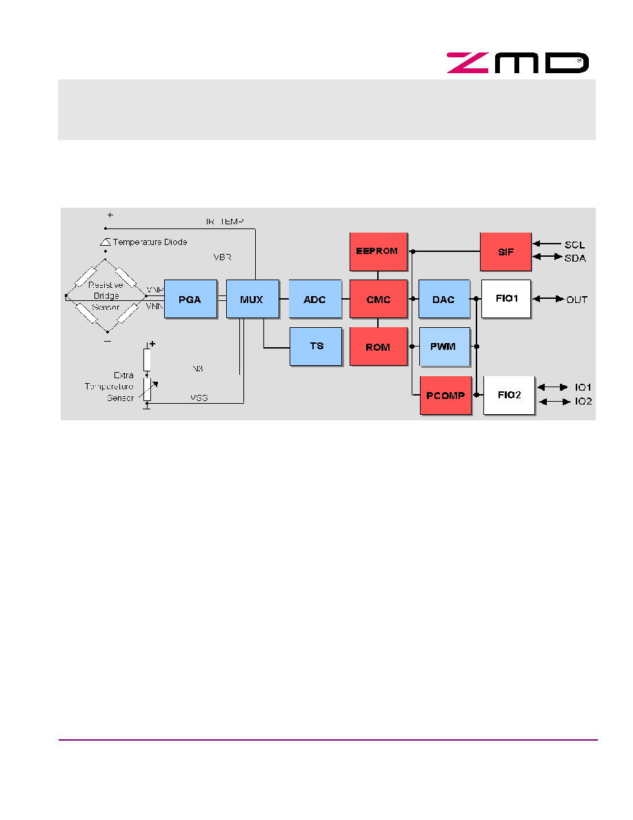
Fig.3: Block diagram of ZMD31050
PGA
programmable gain amplifier
MUX
multiplexer
ADC
analog-to-digital converter
CMC
calibration microcontroller
DAC
digital-to-analog converter
FIO1
flexible I/O 1: analog out (voltage/current), PWM2,
ZACwire
TM
(one-wire-interface)
FIO2
flexible I/O 2: PWM1, SPI data out, SPI slave select, Alarm1, Alarm2SIF
serial interface: I2C data I/O, SPI data in, clock
PCOMP
programmable comparator
EEPROM
for calibration parameters and configuration
TS
on-chip temperature sensor (pn-junction)
ROM
for correction formula and ≠algorithm
PWM
PWM module
The ZMD31050's signal path is partly analog (blue) and partly digital (red). The analog part is realized
differential ≠ this means internal is the differential bridge sensor signal also handled via two signal
lines, which are rejected symmetrically around a common mode potential (analog ground = VDDA/2).
Consequently it is possible to amplify positive and negative input signals, which are located in the
common mode range of the signal input.
The differential signal from the bridge sensor is pre-amplified by the programmable gain amplifier
(PGA). The Multiplexer (MUX) transmits the signals from bridge sensor, external diode or separate
temperature sensor to the ADC in a certain sequence (instead of the temperature diode the internal
pn-junction (TS) can be used optionally). Afterwards the ADC converts these signals into digital values.

Copyright © 2005, ZMD AG, Rev. 0.95, 2005-09-16
4/20
All rights reserved. The material contained herein may not be reproduced, adapted, merged, translated, stored, or used without the prior
written consent of the copyright owner. The Information furnished in this publication is preliminary and subject to changes without notice.
ZMD31050
Advanced Differential Sensor Signal Conditioner
Datasheet
PRELIMINARY
The digital signal correction takes place in the calibration micro-controller (CMC). It is based on a
special correction formula located in the ROM and on sensor-specific coefficients (stored into the
EEPROM during calibration). Dependent on the programmed output configuration the corrected sensor
signal is output as analog value, as PWM signal or in digital format (SPI, I
2
C,
ZACwire
TM
). The output
signal is provided at 2 flexible I/O modules (FIO) and at the serial interface (SIF). The configuration
data and the correction parameters can be programmed into the EEPROM via the digital interfaces.
The modular circuit concept enables fast custom designs varying these blocks and, as a result,
functionality and die size.
1.2
Application Modes
For each application a configuration set has to be established (generally prior to calibration) by
programming the on-chip EEPROM regarding to the following modes:
ß
Sensor channel
-
Sensor mode: ratiometric voltage or current supply mode.
-
Input range: The gain of the analog front end has to be chosen with respect to the maximum
sensor signal span and to this has also adjusted the zero point of the ADC
-
Additional offset compensation: The extended analog offset compensation has to be enabled if
required, e.g. if the sensor offset voltage is near to or larger than the sensor span.
-
Resolution/response time: The A/D converter has to be configured for resolution and converting
scheme (first or second order). These settings influence the sampling rate, signal integration time
and this way the noise immunity. The Sample Order influences the response time too.
-
Ability to invert the sensor bridge inputs
ß
Analog output
-
Choice of output method (voltage value, current loop, PWM) for output register 1.
-
Optional choice of additional output register 2: PWM via IO1 or alarm out module via IO1/2.
ß
Digital communication: The preferred protocol and its parameter have to be set.
ß
Temperature
-
The temperature measure source for the temperature correction has to be chosen.
-
The temperature measure source T1 sensor type
for the temperature correction has to be chosen
(only T1 is usable
for correction!!!)
-
Optional: the temperature measure channel as the second output has to be chosen.
ß
Supply voltage : For non-ratiometric output the voltage regulation has to be configured.
Note: Not all possible combinations of settings are allowed (see section 1.5).
The calibration procedure must include
-
the set of coefficients of calibration calculation
and, depending on configuration,
-
the adjustment of the extended offset compensation,
-
the zero compensation of temperature measurement,
-
the adjustment of the bridge current
and, if necessary,
-
the set of thresholds and delays for the alarms and the reference voltage.

Copyright © 2005, ZMD AG, Rev. 0.95, 2005-09-16
5/20
All rights reserved. The material contained herein may not be reproduced, adapted, merged, translated, stored, or used without the prior
written consent of the copyright owner. The Information furnished in this publication is preliminary and subject to changes without notice.
ZMD31050
Advanced Differential Sensor Signal Conditioner
Datasheet
PRELIMINARY
1.3
Analog Front End (AFE)
The analog front end consists of the programmable gain amplifier (PGA), the multiplexer (MUX) and
the analog-to-digital converter (ADC).
1.3.1.
Programmable Gain Amplifier
The following tables show the adjustable gains, the processable sensor signal spans and the allowed
common mode range.
No.
PGA
Gain a
IN
Gain
Amp1
Gain
Amp2
Gain
Amp3
Max. span
V
IN_SP
in mV/V
Input range
V
IN_CM
in % VDDA
1
420
30
7
2
2
43 - 57
2
280
30
4,66
2
3
40 - 59
3
210
15
7
2
4
43 - 57
4
140
15
4,66
2
6
40 - 59
5
105
15
3,5
2
8
38 - 62
6
70
7,5
4,66
2
12
40 - 59
7
52,5
7,5
3,5
2
16
38 - 62
8
35
3,75
4,66
2
24
40 - 59
9
26,3
3,75
3,5
2
32
38 - 62
10
14
1
7
2
50
43 - 57
11
9,3
1
4,66
2
80
40 - 59
12
7
1
3,5
2
100
38 - 62
13
2,8
1
1,4
2
280
21 - 76
Table 1: Adjustable gains, resulting sensor signal spans and common mode ranges
1.3.2.
Analog Sensor Offset Compensation - Analog Zero Point Shift (AZS)
The ZMD31050 supports two methods of sensor offset cancellation (zero shift):
∑
digital offset correction
∑
analog cancellation for large offset values (up to approx 300% of span)
Digital sensor offset correction will be processed at the digital signal correction/conditioning by the
CMC. Analog sensor offset pre-compensation will be needed for compensation of large offset values,
which would be overdrive the analog signal path by uncompensated gaining. For analog sensor offset
pre-compensation a compensation voltage will be added in the analog pre-gaining signal path (coarse
offset removal). The analog offset compensation in the AFE can be adjusted by 6 EEPROM bits. It
allows an Analog Zero Point Shift up to 300% of the processable signal span.
The zero point shift of the temperature measurements can also be adjusted by 6 EEPROM bits
(Z
AZS
= -25...+25) and is calculated by:
V
AZS
/ VDD
BR
= k * Z
AZS
/ ( 20 * a
IN
)
Bridge in voltage mode, refer "ZMD31050 Functional description" for usable input signal/common mode range at bridge in current mode