 | –≠–ª–µ–∫—Ç—Ä–æ–Ω–Ω—ã–π –∫–æ–º–ø–æ–Ω–µ–Ω—Ç: BU4015B | –°–∫–∞—á–∞—Ç—å:  PDF PDF  ZIP ZIP |
1
Standard ICs
Dual 4-bit static shift register
BU4015B / BU4015BF
The BU4015B and BU4015BF are 4-stage static shift registers, each consisting of two circuits.
The D flip-flops for each stage share a common reset input, enabling external asynchronous reset at any point.
Also, the flip-flops at each stage are triggered by the rising edge of the clock input.
"H" level reset input resets the contents of all stages to "L", regardless of the clock and data input, and sets data out-
puts Q0 to Q3 to "L".
∑
Features
1) Low power dissipation.
2) Wide range of operating power supply voltages.
3) High input impedance.
4) High fan-out.
5) Direct drive of 2 L-TTL inputs and 1 LS-TTL input.
∑
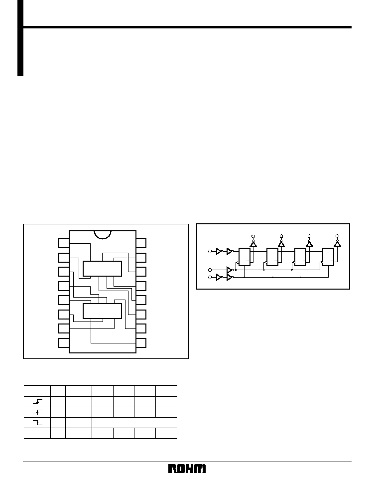
Block diagram
2
Q
3B
Q
1A
Q
0A
D
A
Q
2B
3
4
5
6
RESET
A
7
8
15
14
13
12
11
10
9
V
SS
1
CLOCK
B
D
B
V
DD
Q
0B
Q
1B
Q
2B
Q
3A
RESET
B
CLOCK
A
16
Q
3
Q
2
Q
1
CL
R
D
Q
0
CL
R
D
Q
0
Q
1
Q
2
Q
3
∑
Logic circuit diagram
D
Q
0
Q
1
Q
2
Q
3
CLOCK
RESET
D
Q
CL
Q
R
D
Q
CL
Q
R
D
Q
CL
Q
R
D
Q
CL
Q
R
∑
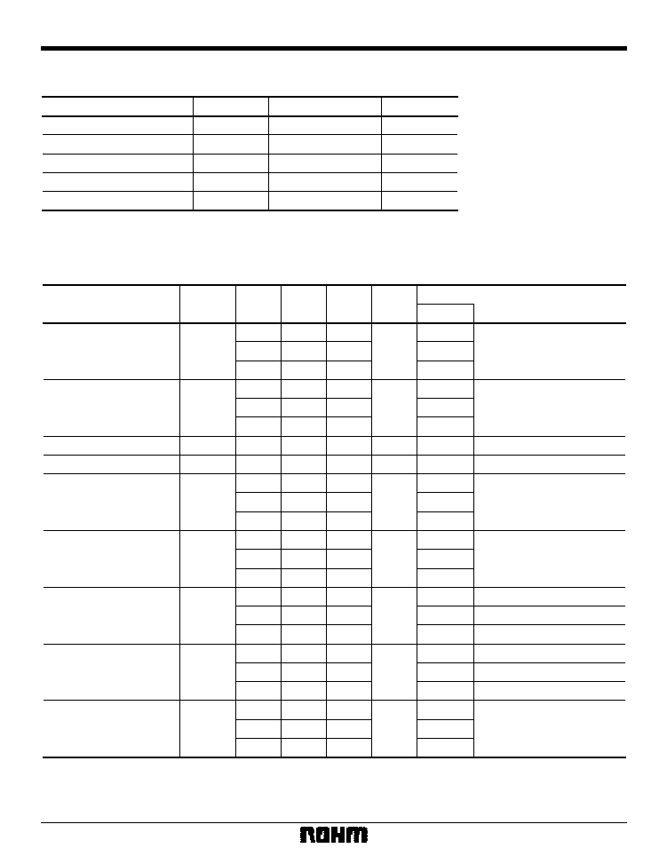
Truth table
CLOCK
D
RESET
Q
0
Q
1
Q
2
Q
3
L
L
L
Q
0
Q
1
Q
2
H
L
H
Q
0
Q
1
Q
2
X
L
No Change
X
X
H
L
L
L
L
X : Irrelevant
2
Standard ICs
BU4015B / BU4015BF
∑
Absolute maximum ratings (V
SS
= 0V, Ta = 25∞C)
Parameter
Symbol
Limits
Unit
Power supply voltage
V
DD
≠ 0.3 ~ + 18
V
Power dissipation
Pd
1000 (DIP), 500 (SOP)
mW
Operating temperature
Topr
≠ 40 ~ + 85
∞
C
Storage temperature
Tstg
≠ 55 ~ + 150
∞
C
Input voltage
V
IN
≠ 0.3 ~ V
DD
+ 0.3
V
∑
Electrical characteristics
DC characteristics (unless otherwise noted, Ta = 25∞C, V
SS
= 0V)
Parameter
Symbol
Min.
Typ.
Max.
Unit
Conditions
V
DD
(V)
Input high level voltage
V
IH
3.5
--
--
V
5
--
7.0
--
--
10
11.0
--
--
15
Input low level voltage
V
IL
--
--
1.5
V
5
--
--
--
3.0
10
--
--
4.0
15
Input high level current
I
IH
--
--
0.3
µ
A
15
V
IH
= 15V
Input low level current
I
IL
--
--
≠ 0.3
µ
A
15
V
IL
= 0V
Output high level voltage
V
OH
4.95
--
--
V
5
I
O
= 0mA
9.95
--
--
10
14.95
--
--
15
Output low level voltage
V
OL
--
--
0.05
V
5
I
O
= 0mA
--
--
0.05
10
--
--
0.05
15
Output high level current
I
OH
≠ 0.16
--
--
mA
5
V
OH
= 4.6V
≠ 0.4
--
--
10
V
OH
= 9.5V
≠ 1.2
--
--
15
V
OH
= 13.5V
Output low level current
I
OL
0.44
--
--
mA
5
V
OL
= 0.4V
1.1
--
--
10
V
OL
= 0.5V
3.0
--
--
15
V
OL
= 1.5V
Static current dissipation
I
DD
--
--
20
µ
A
5
V
I
= V
DD
or GND
--
--
40
10
--
--
80
15
3
Standard ICs
BU4015B / BU4015BF
Switching characteristics (unless otherwise noted, Ta = 25∞C, V
SS
= 0V, C
L
= 50pF)
Parameter
Symbol
Min.
Typ.
Max.
Unit
Conditions
V
DD
(V)
t
TLH
--
180
--
ns
5
--
--
90
--
10
--
65
--
15
t
THL
--
100
--
ns
5
--
--
50
--
10
--
40
--
15
Propagation delay time,
CLOCK, D
Q
t
PLH
t
PHL
--
310
--
ns
5
--
--
125
--
10
--
90
--
15
Propagation delay time,
RESET to Q
t
PLH
t
PHL
--
460
--
ns
5
--
--
180
--
10
--
120
--
15
Setup time
t
su
--
100
--
ns
5
--
--
50
--
10
--
40
--
15
Minimum clock
pulse width
--
185
--
ns
5
--
--
85
--
10
--
55
--
15
Minimum reset
pulse width
--
200
--
ns
5
--
--
80
--
10
--
60
--
15
Maximum clock
frequency
--
20
--
MHz
5
--
--
6.0
--
10
--
7.5
--
15
Maximum clock rise
time and fall time
--
100
--
µ
s
5
--
--
40
--
10
15
--
15
--
Input capacitance
C
IN
--
5
--
pF
--
--
t
WH (CLK)
t
WH (R)
f
(CLK) Max.
t
r (CLK)
t
f (CLK)
Output rise time
Output fall time
4
Standard ICs
BU4015B / BU4015BF
∑
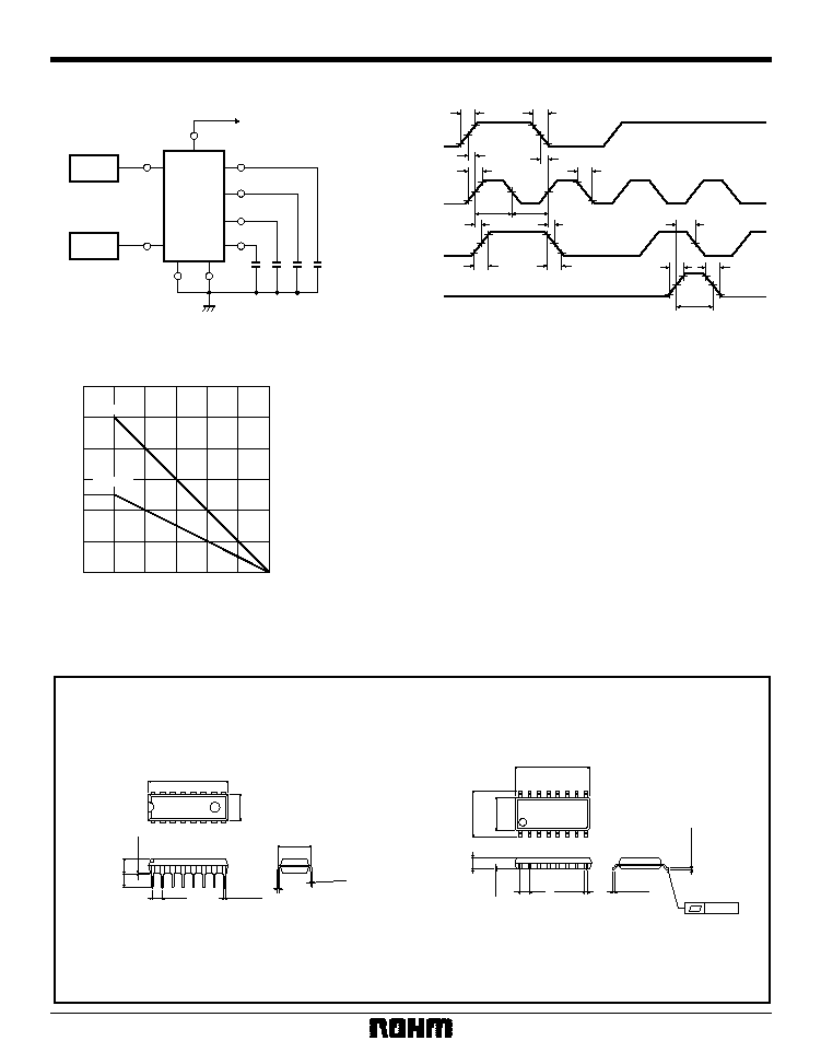
Measurement circuits
Q
3
Q
2
Q
1
CL
R
D
Q
0
P. G. 2
P. G. 1
C
L
V
SS
V
DD
C
L
C
L
C
L
Fig.1 Switching characteristics measurement circuit
GND
CLOCK
RESET
D
Q
0
20ns
20ns
t
PHL
20ns
20ns
20ns
50%
50%
90%
10%
10%
20ns
t
SU
t
SU
t
WH (R)
t
WH
t
WH
t
TLH
t
PLH
t
THL
50%
90%
10%
t
PHL
Fig.2 Switching time measurement waveform
∑
Electrical characterisistic curve
POWER DISSIPATION : Pd (mW)
1200
1000
800
600
400
200
0
0
25
50
75
100
125
150
AMBIENT TEMPERATURE : Ta (
∞
C)
SOP16
DIP16
Fig.3 Power dissipation vs.
ambient temperature
∑
External dimensions (Units: mm)
SOP16
BU4015B
BU4015BF
DIP16
0.4
±
0.1
1.27
0.15
0.15
±
0.1
0.3Min.
4.4
±
0.2
6.2
±
0.3
0.11
1.5
±
0.1
1
16
10.0
±
0.2
8
9
0.51Min.
0.3
±
0.1
9
16
8
1
6.5
±
0.3
3.2
±
0.2
4.25
±
0.3
0.5
±
0.1
19.4
±
0.3
2.54
0
∞
~ 15
∞
7.62